2SK2071-01L中文资料
2SK2071-01L,S N-channel MOS-FET
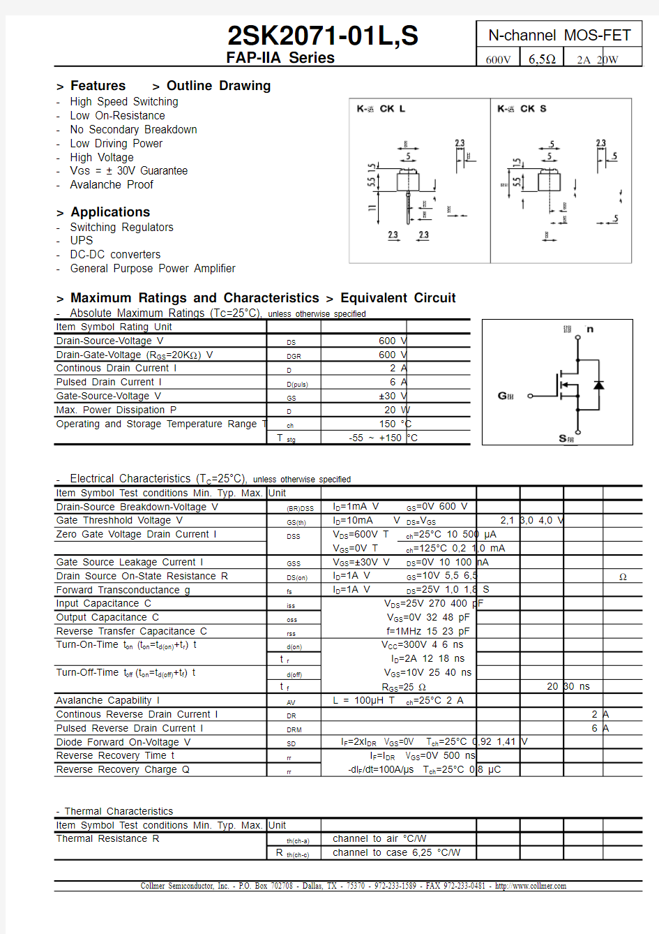
FAP-IIA Series 600V 6,5? 2A 20W >Features > Outline Drawing
-High Speed Switching
-Low On-Resistance
-No Secondary Breakdown
-Low Driving Power
-High Voltage
-V GS = ± 30V Guarantee
-Avalanche Proof
>Applications
-Switching Regulators
-UPS
-DC-DC converters
-General Purpose Power Amplifier
>Maximum Ratings and Characteristics > Equivalent Circuit
-Absolute Maximum Ratings (T C=25°C), unless otherwise specified
Item Symbol Rating Unit
Drain-Source-Voltage V DS 600 V
Drain-Gate-Voltage (R GS=20K?) V DGR 600 V
Continous Drain Current I D 2 A
Pulsed Drain Current I D(puls) 6 A
Gate-Source-Voltage V GS ±30 V
Max. Power Dissipation P D 20 W
Operating and Storage Temperature Range T ch 150 °C
T stg -55 ~ +150 °C
-Electrical Characteristics (T C=25°C), unless otherwise specified
Item Symbol Test conditions Min. Typ. Max. Unit Drain-Source Breakdown-Voltage V(BR)DSS I D=1mA V GS=0V 600 V Gate Threshhold Voltage V GS(th) I D=10mA V DS=V GS 2,1 3,0 4,0 V Zero Gate Voltage Drain Current I DSS V DS=600V T ch=25°C 10 500 μA
V GS=0V T ch=125°C 0,2 1,0 mA Gate Source Leakage Current I GSS V GS=±30V V DS=0V 10 100 nA Drain Source On-State Resistance R DS(on) I D=1A V GS=10V 5,5 6,5 ?Forward Transconductance g fs I D=1A V DS=25V 1,0 1,8 S Input Capacitance C iss V DS=25V 270 400 pF Output Capacitance C oss V GS=0V 32 48 pF Reverse Transfer Capacitance C rss f=1MHz 15 23 pF Turn-On-Time t on (t on=t d(on)+t r) t d(on)V CC=300V 4 6 ns
t r I D=2A 12 18 ns Turn-Off-Time t off (t on=t d(off)+t f) t d(off)V GS=10V 25 40 ns
t f R GS=25 ? 20 30 ns Avalanche Capability I AV L = 100μH T ch=25°C 2 A Continous Reverse Drain Current I DR 2 A Pulsed Reverse Drain Current I DRM 6 A Diode Forward On-Voltage V SD I F=2xI DR V GS=0V T ch=25°C 0,92 1,41 V Reverse Recovery Time t rr I F=I DR V GS=0V 500 ns Reverse Recovery Charge Q rr -dI F/dt=100A/μs T ch=25°C 0,8 μC
- Thermal Characteristics
Item Symbol Test conditions Min. Typ. Max. Unit Thermal Resistance R th(ch-a) channel to air °C/W
R th(ch-c) channel to case 6,25 °C/W Collmer Semiconductor, Inc. - P.O. Box 702708 - Dallas, TX - 75370 - 972-233-1589 - FAX 972-233-0481 - https://www.360docs.net/doc/f71909857.html,
N-channel MOS-FET
2SK2071-01L,S
600V
6,5?
2A 20W
FAP-IIA Series
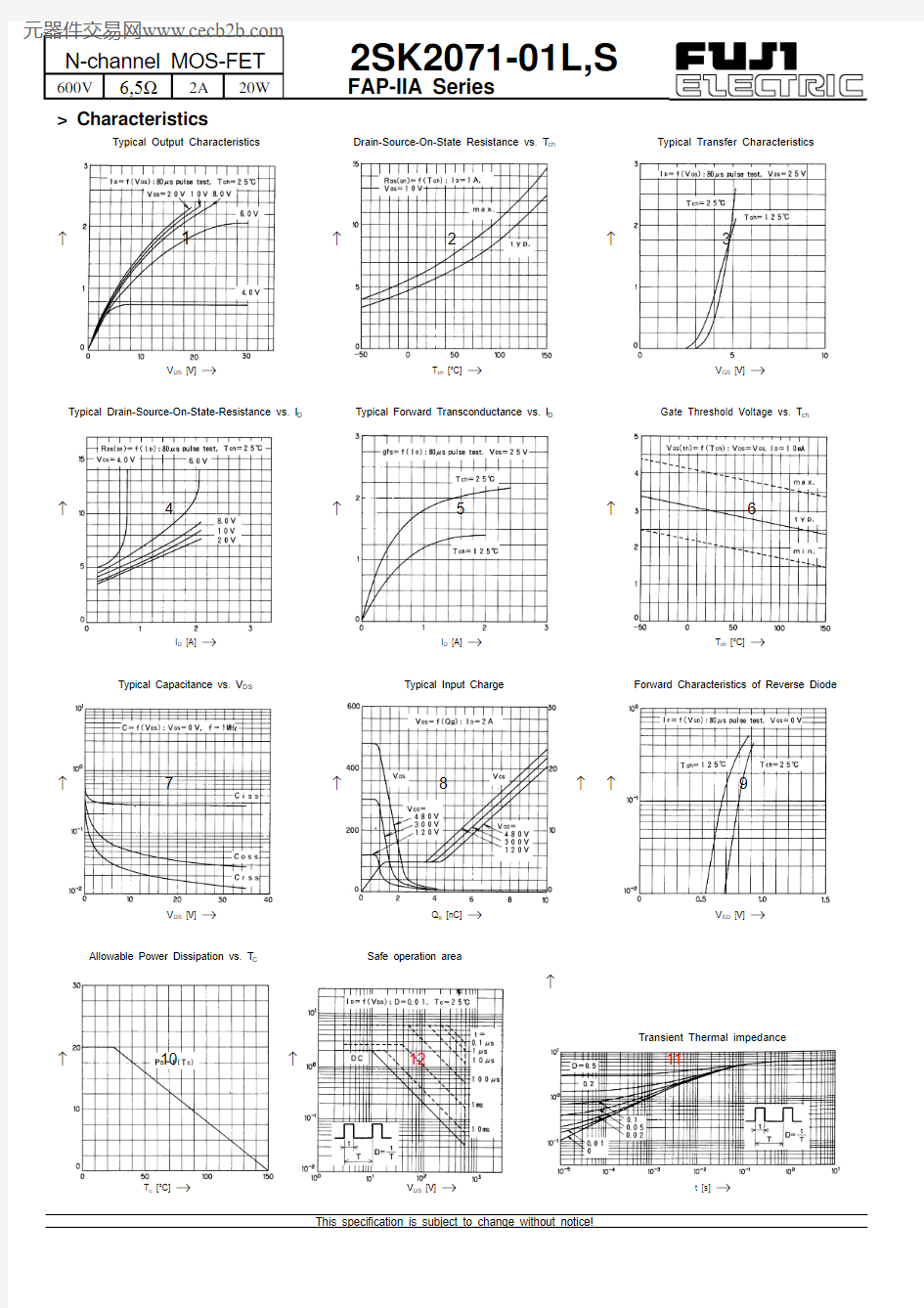
> Characteristics
Typical Output Characteristics
Drain-Source-On-State Resistance vs. T ch
Typical Transfer Characteristics
↑
1
↑
2↑
3
I D [A ]
R D S (O N ) [?]
I D [A ]
V DS [V]
→
T ch [°C]
→
V GS [V]
→
Typical Drain-Source-On-State-Resistance vs. I D Typical Forward Transconductance vs. I D Gate Threshold Voltage vs. T ch
↑
4↑
5↑
6
R D S (O N ) [?]
g f s [S ]
V G S (t h ) [V ]
I D [A]
→
I D [A]
→
T ch [°C]
→
Typical Capacitance vs. V DS Typical Input Charge Forward Characteristics of Reverse Diode
↑
7↑
8↑
↑
9
C [n F ]
V D S [V ]
V G S [V ]
I F [A ]
V DS [V]
→
Q g [nC]
→
V SD [V]
→
Allowable Power Dissipation vs. T C Safe operation area
↑
Z t h (c h -c ) [K /W ]
Transient Thermal impedance
↑
10↑
1211
P D [W ]
I D [A ]
T c [°C]
→
V DS [V]
→
t [s]
→
This specification is subject to change without notice!
元器件交易网https://www.360docs.net/doc/f71909857.html,