TK5561A-PP
Features Array?65 ms Cycle Time for Crypto Algorithm Programming
?Encryption Time < 10 ms, < 30 ms Optional
?Identification Transponder in Plastic Cube
?Contactless Read/Write Data Transmission
?High-security Crypto Algorithm Optional
?Inductive Coupled Power Supply at 125 kHz
?Basic Component R/W e5561 IDIC?
?Built-in Coil and Capacitor for Circuit Antenna
?Starts with Cyclical Data Read Out
?Programmable Adaption of Resonance Frequency
?128-bit User-programmable EEPROM
?Typical < 50 ms to Write and Verify a Block
?Read/Write Protection by Lock Bits
?Options Set by EEPROM:
–Bit Rate (Bit/s): Rf/32, Rf/64
–Modulation: Manchester, Bi-phase
Application
?Car Immobilizers with Higher Security Level
?High-security Identification Systems
1.Description
The TK5561A-PP is a complete transponder integrating all important functions for immobilizer and identification systems. It consists of a plastic cube which accommo-dates the crypto IDIC e5561A and the antenna realized as tuned LC-circuit. The TK5561A-PP is a R/W crypto transponder for applications which demand higher secu-rity levels than those which standard R/W transponders can fulfil. For this reason, the TK5561A-PP has an additional encryption algorithm block which enables a base sta-tion to authenticate the transponder. Any attempt to fake the base station with a wrong transponder will be recognized immediately. For authentication, the base station transmits a challenge to the TK5561A-PP. This challenge is encrypted by both the IC and the base station. Both should possess the same secret key. Only then can the results be expected to be equal.
For detailed technical information about functions, configurations etc., please refer to
the e5561 data sheet.
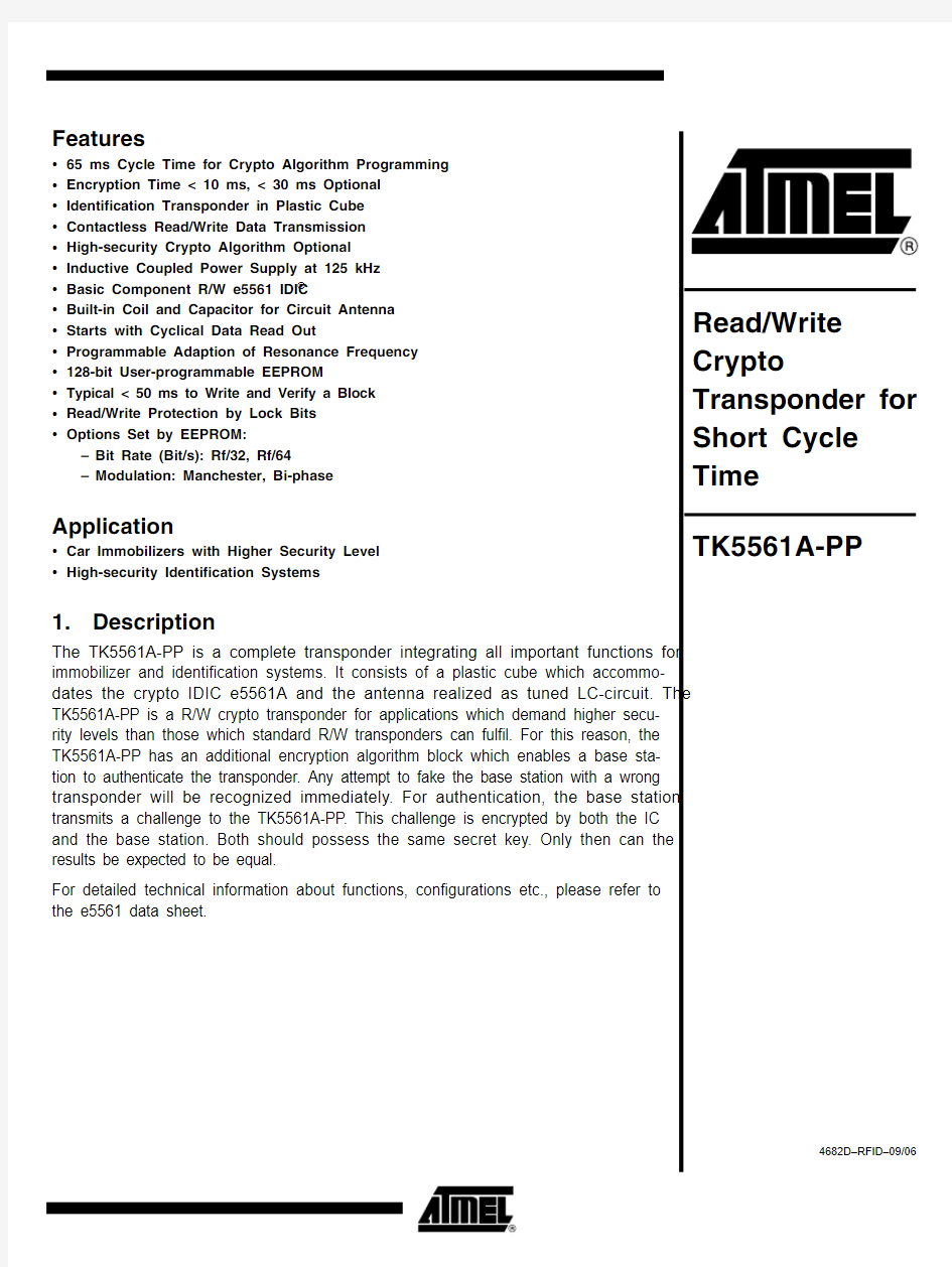
Figure 1-1.Transponder and Base Station
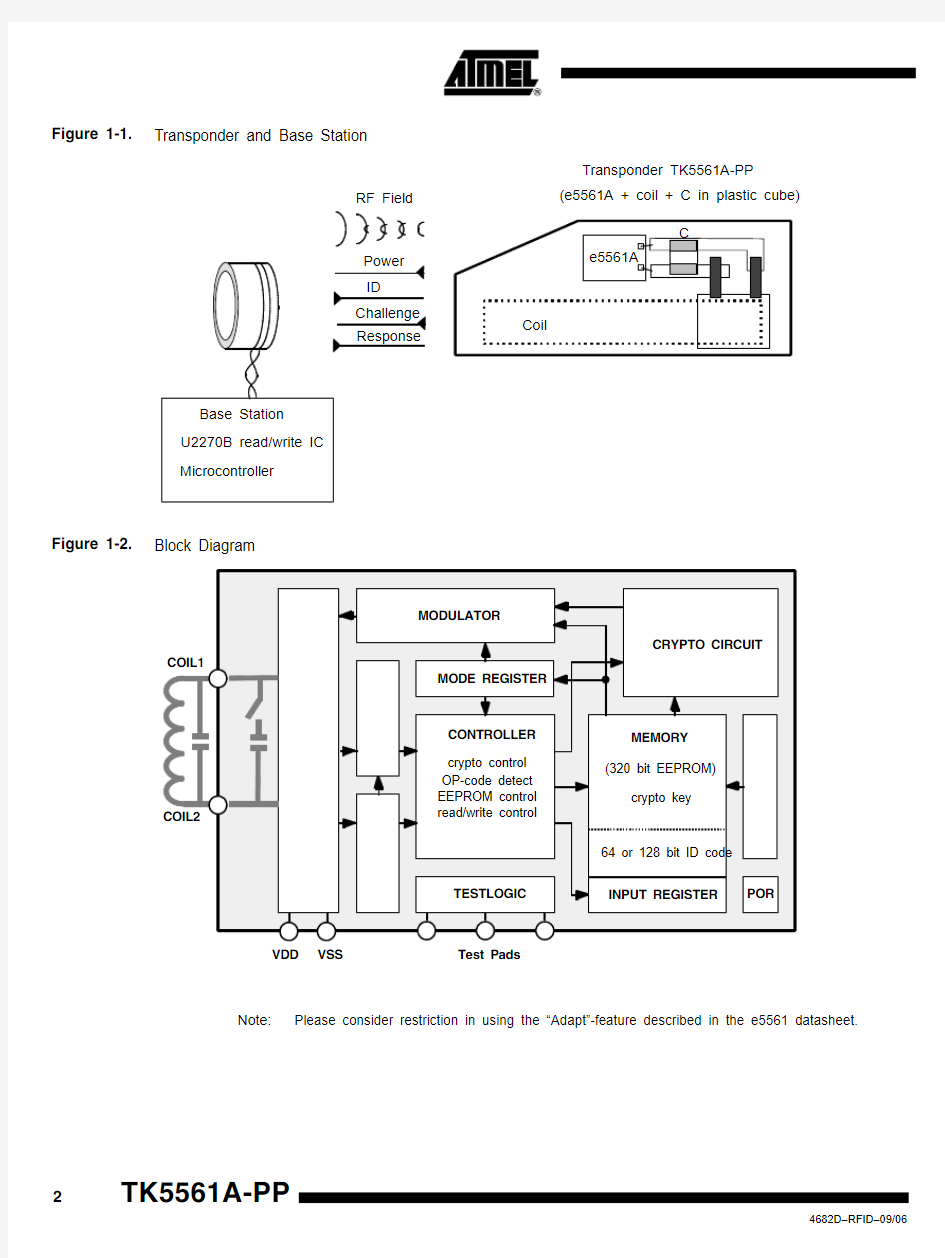
Figure 1-2.Block Diagram
Note:Please consider restriction in using the “Adapt”-feature described in the e5561 datasheet. 2TK5561A-PP
TK5561A-PP
2.General
The transponder is the mobile part of the closed coupled identification system (see Figure 1-1),
whereas the read/write base station is based on the U2270B or on discrete solutions, and the
read/write transponder is based on the e5561A IDIC.
The transponder is a plastic-cube device consisting of the following parts:
?The transponder antenna, with a tuned LC-circuit
?Read/write IDIC(e5561A) with EEPROM
3.Transponder Antenna
The antenna consists of a coil and a capacitor for tuning the circuit to the nominal carrier fre-
quency of 125kHz. The coil has a ferrite core to improve the read, write and programming
operation distances.
4.Read/Write Crypto Identification
The e5561A is a member of the Atmel?'s contactless ID entification IC (IDIC) family, which are
used in applications where information has to be transmitted without contacts. The IDIC is con-
nected to a tuned LC circuit for power supply and bidirectional data communication (R ead/W rite)
to a base station.
The on-chip non-volatile memory of the 320-bit EEPROM (10 blocks, 32 bits each) can be read
and written blockwise by a read/write base station, e.g. based on the U2270B. Up to four blocks
consisting of the user programmable ID code, the crypto key and configurations are stored in six
blocks. The crypto key and the ID code can be individually protected against overwriting.
The typical operational frequency of the TK5561A-PP is 125 kHz. Two data bit rates are pro-
grammable: Rf/32 and Rf/64. During the reading operation the incoming RF field is dampened
bit-wise by an on-chip load. This AM-modulation is detected by the field generating base station
unit. Data transmission starts after power-up with the transmission of the ID code and continues
as long as the TK5561A-PP is powered.
Writing is carried out by means of Atmel's patented writing method. To transmit data to the
TK5561A-PP the read/write base station has to interrupt the RF field for a short time to create a
field gap. The information is encoded in the number of clock cycles between two subsequent
gaps.
See the e5561A data sheet for detailed information of the IDIC.
3
4
TK5561A-PP
5.Absolute Maximum Ratings
Stresses beyond those listed under “Absolute Maximum Ratings” may cause permanent damage to the device. This is a stress rating only and functional operation of the device at these or any other conditions beyond those indicated in the operational sections of this specification is not implied. Exposure to absolute maximum rating conditions for extended periods may affect device reliability.Parameter
Symbol Value Unit Operating temperature range T amb –40 to +85°C Storage temperature range
T stg –40 to +125
°C Maximum assembly temperature, t < 5 min T ass 170°C Magnetic field strength at 125 kHz
H pp
1000
A/m
6.Operating Characteristics Transponder
T amb = 25°C, f = 125 kHz unless otherwise specified Parameters Test Conditions
Symbol
Min.
Typ.Max.
Unit Inductance
L
4.2
mH
LC Circuit, H pp = 20 A/m Resonance frequency T amb = –40 to +85°C
f r 121125129kHz
Quality factor
Q LC
5
8
11
Magnetic Field Strength (H)Maximum field strength where transponder does not modulate No influence to other transponders in the field
H pp not
5
A/m
Minimum Field Strength (H)
Read mode
T amb = –40°C
H pp –4024A/m T amb = 25°C H pp 2518A/m T amb = 85°C H pp 8515A/m Programming mode T amb = –40°C
H pp –4030A/m T amb = 25°C H pp 2535A/m T amb = 85°C
H pp 8540A/m Lowest adapt frequency f LA 118121124.5kHz Highest adapt frequency f HA 125128
131.5
kHz Data retention EEPROM T = 25°C t retention
10Y ears
Programming cycles EEPROM 100,000
Programming time/block RF = 125 kHz
t p 16
ms Maximum field strength
H pp max
600
A/m
TK5561A-PP Figure 6-1.Typical Curve for Degree of Modulation
Figure 6-2.
Measurement of the Degree of Modulation
m V1V2
–
V1V2
+
--------------------
=
5
7.Measurement Assembly
All parameters are measured in a Helmholtz-arrangement, which generates a homogenous
magnetic field (see Figure 7-1 and Figure 7-2). A function generator drives the field generating
coils, so the magnetic field can be varied in frequency and field strength.
Figure 7-1.Testing Application
Figure 7-2.Testing Geometry
6TK5561A-PP
TK5561A-PP
8.Writing Data into the TK5561A-PP
A write sequence of the TK5561A-PP is shown in Figure 8-1. Writing data into the transponder
occurs by interrupting the RF field with short gaps. After the start gap the write opcode (10) is
transmitted. The next 32 bits contain the actual data. The last 4 bits denote the destination block
address. If the correct number of bits have been received, the actual data is programmed into
the specified memory block.
Figure 8-1.Write Protocol to Program the EEPROM
9.Writing Data Decoding
The time elapsing between two detected gaps is used to encode the information. As soon as a
gap is detected, a counter starts counting the number of field clock cycles until the next gap is
detected. Depending on how many field clocks elapse, the data is regarded as 0 or 1. The
required number of field clocks is shown in Figure 9-1. A valid 0 is assumed if the number of
counted clock periods is between 16 and 31, for a valid 1 it is 48 or 63 respectively. Any other
value being detected results in an error and the device exits write mode and returns to read
mode.
Figure 9-1.Write Data Decoding Scheme
7
10.Actual Device Behavior
The TK5561A-PP detects a gap if the voltage across the coils decreases below a peak-to-peak
value of about 800 mV. Until then, the clock pulses are counted. The number given for a valid 0
or 1 (see Figure 9-1 on page 7) refers to the actual clock pulses counted by the device. How-
ever, there are always more clock pulses being counted than were applied by the base station.
The reason for this is the fact that an RF field cannot be switched off immediately. The coil volt-
age decreases exponentially. So although the RF field coming from the base station is switched
off, it takes some time until the voltage across the coils reaches the threshold peak-to-peak
value of about 800 mV and the device detects the gap. Referring to the following diagram Figure
10-1, this means that the device uses the times t0 internal and t1 internal. The exact times for t0
and t1 are dependent on the application (e.g., field strength, etc.)
Typical time frames are:
t0 = 60 to 140 μs
t1 = 300 to 400 μs
t gap = 150 to 400 μs
Antennas with a high Q-factor require longer times for t gap and shorter time values for t0 and t1. Figure 10-1.Ideal and Actual Signal Behavior
11.Operating Distance
The maximum distance between the base station and the TK5561A-PP depends mainly on the
base station, the coil geometries and the chosen modulation options. Typical distances are 0 to
3cm. A general maximum distance value cannot be given. A convenient way is to measure the
TK5561A-PP within its environment. Rules for a correct base-station design can be provided
upon request (see Antenna Design Guide).
8TK5561A-PP
TK5561A-PP 12.Application
Figure https://www.360docs.net/doc/f27518037.html,plete Transponder System with the U2270B Read/Write IC
9
10
TK5561A-PP
13.Mechanical Specification
Figure 13-1.Mechanical Drawing of Transponder
15.
Revision History
14.Ordering Information
Extended Type Number Package
Remarks
TK5561A-PP
–
A = Version of e5561 IDIC
Please note that the following page numbers referred to in this section refer to the specific revision mentioned, not to this document.Revision No.
History
4682D-RFID-09/06
? Put datasheet in a new template ? Pb-free logo on page 1 deleted ? Features on page 1 changed ? Note on page 2 added
4682C-RFID-06/05
? Lead-free Logo on page 1 added
4682B-RFID-05/05
? Put datasheet in a new template
? Figure 1.1 “T ransponder and Base Station” on page 2 changed
? Figure 6.1 “T ypical Curve for Degree of Modulation” on page 5 changed ? Figure 12.1 “Complete T ransponder System with the U2270B Read/Write IC” on page 9 changed
Disclaimer: The information in this document is provided in connection with Atmel products. No license, express or implied, by estoppel or otherwise,to any intellectual property right is granted by this document or in connection with the sale of Atmel products. EXCEPT AS SET FORTH IN ATMEL ’S TERMS AND CONDI-TIONS OF SALE LOCATED ON ATMEL ’S WEB SITE, ATMEL ASSUMES NO LIABILITY WHATSOEVER AND DISCLAIMS ANY EXPRESS, IMPLIED OR STATUTORY WARRANTY RELATING TO ITS PRODUCTS INCLUDING, BUT NOT LIMITED TO, THE IMPLIED WARRANTY OF MERCHANTABILITY, FITNESS FOR A PARTICULAR PURPOSE, OR NON-INFRINGEMENT. IN NO EVENT SHALL ATMEL BE LIABLE FOR ANY DIRECT, INDIRECT, CONSEQUENTIAL, PUNITIVE, SPECIAL OR INCIDEN-TAL DAMAGES (INCLUDING, WITHOUT LIMITATION, DAMAGES FOR LOSS OF PROFITS, BUSINESS INTERRUPTION, OR LOSS OF INFORMATION) ARISING OUT OF THE USE OR INABILITY TO USE THIS DOCUMENT, EVEN IF ATMEL HAS BEEN ADVISED OF THE POSSIBILITY OF SUCH DAMAGES. Atmel makes no representations or warranties with respect to the accuracy or completeness of the contents of this document and reserves the right to make changes to specifications and product descriptions at any time without notice. Atmel does not make any commitment to update the information contained herein. Unless specifically provided otherwise, Atmel products are not suitable for, and shall not be used in, automotive applications. Atmel’s products are not intended, authorized, or warranted for use as components in applications intended to support or sustain life.
Atmel Corporation
Atmel Operations
2325 Orchard Parkway San Jose, CA 95131, USA Tel: 1(408) 441-0311Fax: 1(408) 487-2600
Regional Headquarters
Europe
Atmel Sarl
Route des Arsenaux 41Case Postale 80CH-1705 Fribourg Switzerland
Tel: (41) 26-426-5555Fax: (41) 26-426-5500
Asia
Room 1219
Chinachem Golden Plaza 77 Mody Road Tsimshatsui East Kowloon Hong Kong
Tel: (852) 2721-9778Fax: (852) 2722-1369
Japan
9F, Tonetsu Shinkawa Bldg.1-24-8 Shinkawa
Chuo-ku, Tokyo 104-0033Japan
Tel: (81) 3-3523-3551Fax: (81) 3-3523-7581
Memory
2325 Orchard Parkway San Jose, CA 95131, USA Tel: 1(408) 441-0311Fax: 1(408) 436-4314
Microcontrollers
2325 Orchard Parkway San Jose, CA 95131, USA Tel: 1(408) 441-0311Fax: 1(408) 436-4314
La Chantrerie BP 70602
44306 Nantes Cedex 3, France Tel: (33) 2-40-18-18-18Fax: (33) 2-40-18-19-60
ASIC/ASSP/Smart Cards
Zone Industrielle
13106 Rousset Cedex, France Tel: (33) 4-42-53-60-00Fax: (33) 4-42-53-60-01
1150 East Cheyenne Mtn. Blvd.Colorado Springs, CO 80906, USA Tel: 1(719) 576-3300Fax: 1(719) 540-1759
Scottish Enterprise Technology Park Maxwell Building
East Kilbride G75 0QR, Scotland Tel: (44) 1355-803-000Fax: (44) 1355-242-743
RF/Automotive
Theresienstrasse 2Postfach 3535
74025 Heilbronn, Germany Tel: (49) 71-31-67-0
Fax: (49) 71-31-67-2340
1150 East Cheyenne Mtn. Blvd.Colorado Springs, CO 80906, USA Tel: 1(719) 576-3300Fax: 1(719) 540-1759
Biometrics/Imaging/Hi-Rel MPU/High-Speed Converters/RF Datacom
Avenue de Rochepleine BP 123
38521 Saint-Egreve Cedex, France Tel: (33) 4-76-58-30-00Fax: (33) 4-76-58-34-80
Literature Requests
https://www.360docs.net/doc/f27518037.html,/literature
? 2006 Atmel Corporation . All rights reserved. Atmel ?, logo and combinations thereof, Everywhere You Are ?, IDIC ?, and others are regis-tered trademarks or trademarks of Atmel Corporation or its subsidiaries. Other terms and product names may be trademarks of others.