ZXTN25020DZTA;中文规格书,Datasheet资料
ZXTN2011ZTA资料

S E M I C O N D U C T O R SSUMMARYBV CEO = 100V :R SAT = 31m ; I C = 4.5A DESCRIPTIONPackaged in the SOT89outline this new low saturation 100V NPN transistor offers extremely low on state losses making it ideal for use in DC-DC circuits and various driving and power management functions.FEATURES• 4.5 amps continuous current •Up to 10 amps peak current •Very low saturation voltagesAPPLICATIONS•Motor driving •Line switching •High side switches•Subscriber line interface cards (SLIC)DEVICE MARKING853ZXTN2011ZISSUE 2 - MAY 2006100V NPN LOW SATURATION MEDIUM POWER TRANSISTOR IN SOT891SOT89PINOUTVIEWDEVICE REEL SIZE TAPE WIDTH QUANTITY PERREEL ZXTN2011ZTA7"12mm embossed1,000 unitsORDERING INFORMATIONZXTN2011ZS E M I C O N D U C T O R SISSUE 2 - MAY 2006 2PARAMETER SYMBOL LIMIT UNIT Collector base voltage BV CBO200V Collector emitter voltage BV CEO100V Emitter base voltage BV EBO7V Continuous collector current(a)I C 4.5A Peak pulse current I CM10APower dissipation at T A=25°C(a) Linear derating factor P D 1.512WmW/°CPower dissipation at T A=25°C(b) Linear derating factor P D 2.116.8WmW/°COperating and storage temperature range T j,T stg-55 to +150°C ABSOLUTE MAXIMUM RATINGSPARAMETER SYMBOL LIMIT UNIT Junction to ambient(a)RJA83°C/W Junction to ambient(b)RJA60°C/WNOTES:(a)For a device surface mounted on 25mm x 25mm x 1.6mm FR4 PCB with high coverage of single sided 1oz copper, in still air conditions.(b)For a device surface mounted on 50mm x 50mm x 1.6mm FR4 PCB with high coverage of single sided 1oz copper, in still air conditions. THERMAL RESISTANCEZXTN2011ZS E M I C O N D U C T O R SISSUE 2 - MAY 20063ZXTN2011ZS E M I C O N D U C T O R SISSUE 2 - MAY 2006 4PARAMETER SYMBOL MIN.TYP.MAX.UNIT CONDITIONS Collector base breakdown voltage BV CBO200235V I C=100A Collector emitter breakdown voltage BV CER200235V I C=1A,RBՅ1k⍀Collector emitter breakdown voltage BV CEO100115V I C=10mA*Emitter base breakdown voltage BV EBO78.1V I E=100ACollector cut-off current I CBO500.5nAAV CB=150VV CB=150V,T amb=100ЊCCollector cut-off current I CERRՅ1k⍀1000.5nAAV CB=150VV CB=150V,T amb=100ЊCEmitter cut-off current I EBO10nA V EB=6VCollector-emitter saturation voltage V CE(SAT)2045851553060115195mVmVmVmVI C=0.1A,I B=5mA*I C=1A,I B=100mA*I C=2A,I B=100mA*I C=5A,I B=500mA*Base emitter saturation voltage V BE(SAT)10001100mV I C=5A,I B=500mA* Base emitter turn on voltage V BE(ON)9001000mV I C=5A,V CE=2V*Static forward current transfer ratio h FE10010030102302006020300I C=10mA,V CE=2V*I C=2A,V CE=2V*I C=5A,V CE=2V*I C=10A,V CE=2V*Transition frequency f T130MHz I C=100mA,V CE=10Vf=50MHzOutput capacitance C OBO26pF V CB=10V,f=1MHz*Switching times t ONt OFF411010ns I C=1A,V CC=10V,I B1=I B2=100mAELECTRICAL CHARACTERISTICS(at T amb= 25°C unless otherwise stated) * Measured under pulsed conditions. Pulse widthՅ300s; duty cycleՅ2%.ZXTN2011ZS E M I C O N D U C T O R SISSUE 2 - MAY 20065ZXTN2011ZS E M I C O N D U C T O R S6ISSUE 2 - MAY 2006EuropeZetex GmbHStreitfeldstraße 19D-81673 München GermanyTelefon: (49) 89 45 49 49 0Fax: (49) 89 45 49 49 49europe.sales@AmericasZetex Inc700 Veterans Memorial Hwy Hauppauge, NY 11788USATelephone: (1) 631 360 2222Fax: (1) 631 360 8222usa.sales@Asia PacificZetex (Asia) Ltd3701-04Metroplaza Tower 1Hing Fong Road, Kwai Fong Hong KongTelephone: (852) 26100 611Fax: (852) 24250 494asia.sales@Corporate Headquarters Zetex Semiconductors plc Zetex Technology ParkChadderton, Oldham, OL9 9LL United KingdomTelephone (44) 161 622 4444Fax: (44) 161 622 4446hq@These offices are supported by agents and distributors in major countries world-wide.This publication is issued to provide outline information only which (unless agreed by the Company in writing)may not be used,applied or reproduced for any purpose or form part of any order or contract or be regarded as a representation relating to the products or services concerned.The Company reserves the right to alter without notice the specification, design, price or conditions of supply of any product or service.For the latest product information,log on to ©ZetexSemiconductors plc 2005。
ZXT4M322TA;中文规格书,Datasheet资料

PARAMETER
SYMBOL MIN. TYP. MAX. UNIT CONDITIONS
Collector-Base Breakdown Voltage Collector-Emitter Breakdown Voltage Emitter-Base Breakdown Voltage Collector Cut-Off Current Emitter Cut-Off Current Collector Emitter Cut-Off Current Collector-Emitter Saturation Voltage
(b) For a single device surface mounted on 10 sq cm 1oz copper on FR4 PCB, in still air conditions measured at tՅ5 secs with all exposed pads attached.
Transition Frequency
fT
-70 -150
V IC=-100A
-70 -125
V IC=-10mA*
-7.5 -8.5
V IE=-100A
-25 nA VCB=-55V
-25 nA VEB=-6V
-25 nA VCE=-55V
-35 -135 -140 -175
-50 -200 -220 -260
Output Capacitance Turn-On Time Turn-Off Time
Cobo t(on) t(off)
14
20
pF VCB=-10A, f=1MHz
40
ns VCC=-50V, IC=-1A
700
IRFP250NPBF;中文规格书,Datasheet资料
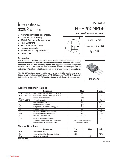
IRFP250NPbFHEXFET ® Power MOSFET08/18/10ParameterMax.UnitsI D @ T C = 25°C Continuous Drain Current, V GS @ 10V 30I D @ T C = 100°C Continuous Drain Current, V GS @ 10V 21A I DMPulsed Drain Current 120P D @T C = 25°C Power Dissipation 214W Linear Derating Factor 1.4W/°C V GS Gate-to-Source Voltage± 20V E AS Single Pulse Avalanche Energy 315mJ I AR Avalanche Current30A E AR Repetitive Avalanche Energy 21mJ dv/dt Peak Diode Recovery dv/dt 8.6V/ns T J Operating Junction and-55 to +175T STGStorage Temperature RangeSoldering Temperature, for 10 seconds 300 (1.6mm from case )°CMounting torque, 6-32 or M3 srew10 lbf•in (1.1N•m)Absolute Maximum RatingsParameterTyp.Max.UnitsR θJC Junction-to-Case–––0.7R θCS Case-to-Sink, Flat, Greased Surface 0.24–––°C/WR θJAJunction-to-Ambient–––40Thermal Resistance 1Descriptionl Advanced Process Technology l Dynamic dv/dt Ratingl 175°C Operating Temperature l Fast Switchingl Fully Avalanche Rated l Ease of Parallelingl Simple Drive Requirements TO-247AClLead-FreePD - 95007AIRFP250NPbFSource-Drain Ratings and CharacteristicsStarting T J = 25°C, L = 1.9mHR G = 25Ω, I AS = 18A. (See Figure 12)Repetitive rating; pulse width limited by max. junction temperature. (See Fig. 11)Notes:I SD ≤ 18A , di/d t ≤ 374A/µs, V DD ≤ V (BR)DSS ,T J ≤ 175°CPulse width ≤ 300µs; duty cycle ≤ 2%.Electrical Characteristics @ T = 25°C (unless otherwise specified)IRFP250NPbF 3Vs. TemperatureIRFP250NPbF4Fig 5. Typical Capacitance Vs.Drain-to-Source VoltageFig 6.Gate-to-Source VoltageForward VoltageTypical Gate Charge Vs.1101001000V DS , Drain-to-Source Voltage (V)010002000300040005000C , C a p a c i t a n c e (p F )IRFP250NPbF5Fig 9. Maximum Drain Current Vs.Fig 10a. Switching Time Test CircuitV V d(on)rd(off)fFig 10b. Switching Time WaveformsFig 11. Maximum Effective Transient Thermal Impedance, Junction-to-CaseDDIRFP250NPbF6VDSCurrent Sampling Resistors10 VFig 13b. Gate Charge Test CircuitFig 13a. Basic Gate Charge Waveform Fig 12b. Unclamped Inductive WaveformsI ASVs. Drain CurrentV DDIRFP250NPbF7Fig 14. For N-Channel HEXFETS* V GS = 5V for Logic Level DevicesPeak Diode Recovery dv/dt Test CircuitV DDIRFP250NPbFData and specifications subject to change without notice.233 Kansas St., El Segundo, California 90245, USA Tel: (310) 252-7105TAC Fax: (310) 252-7903Visit us at for sales contact information .08/2010分销商库存信息: IRIRFP250NPBF。
P0250.104NLT;P0250.103NLT;P0250.222NLT;P0250.474NLT;P0250.223NLT;中文规格书,Datasheet资料

1 2
Weight . . . . . . . . 3.6 grams Tape & Reel. . . . . . 250/reel
.291 7,39 .762 19,35
1.260 ± .012 32,00 ± 0,30
Dimensions: Inches mm
Unless otherwise specified, all tolerances are ± .010
P0250.473NL
47
2.6
P0250.683NL
Байду номын сангаас
68
2.3
P0250.104NL
100
1.8
P0250.154NL
150
1.5
P0250.224NL
220
1.2
P0250.334NL
330
1.0
P0250.474NL
470
.82
P0250.684NL
680
.72
P0250.105NL
1000
.56
0,25
TAPE & REEL LAYOUT
.620 15,75
.945 24,00
USER DIRECTION OF FEED
USA 858 674 8100 • Germany 49 7032 7806 0 • Singapore 65 6287 8998 • Shanghai 86 21 54643211 / 2 • China 86 755 33966678 • Taiwan 886 3 4641811
P0250.222NLT P0250.684NLT P0250.333NLT P0250.102NLT P0250.224NLT
UMT2NTR;中文规格书,Datasheet资料

TransistorsRev.A 1/2General purpose (dual transistors)EMT2 / UMT2N / IMT2Az Features1) Two 2SA1037AK chips in a EMT or UMT or SMT package.z Equivalent circuitsz Absolute maximum ratings (T a=25°C)ParameterSymbol V CBO V CEO V EBO I CP C Tj TstgLimits −60−50−6−150300(TOTAL)150(TOTAL)EMT2 / UMT2N IMT2A150−55 to +150Unit V V V mA mW°C °CCollector-base voltage Collector-emitter voltage Emitter-base voltage Collector current Collector power dissipationJunction temperature Storage temperature∗1 120mW per element must not be exceeded.∗2 200mW per element must not be exceeded.∗1∗2z Package, marking, and packaging specificationsEMT2EMT6T2T2R 8000IMT2A SMT6T2T1083000UMT2N UMT6T2TR 3000Type Package Marking CodeBasic ordering unit (pieces)z External dimensions (Unit : mm)z Electrical characteristics (T a=25°C)ParameterSymbol Min.Typ.Max.Unit ConditionsTransition frequency BV CBO BV CEO BV EBO I CBO I EBO V CE(sat)h FE f T −60−50−6−−−120−−−−−−−−140−−−−0.1−0.1−0.5560−V V V µA µA V −MHz ∗Cob−45pFI C =−50µA I C =−1mA I E =−50µA V CB =−60V V EB =−6VV CE =−12V, I E =2mA, f =100MHz V CE =−12V, I E =0A, f =1MHzI C /I B =−50mA/−5mA V CE =−6V, I C =−1mA∗Transition frequency of the device.Collector-base breakdown voltage Collector-emitter breakdown voltage Emitter-base breakdown voltage Collector cutoff current Emitter cutoff currentCollector-emitter saturation voltage DC current transfer ratio Output capacitanceTransistors Rev.A 2/2z Electrical characteristics curvesFig.1 Grounded emitter propagationcharacteristics C O L L E C T O R C U R R E N T : I c (m A )−−−−−−−−−BASE TO EMITTER VOLTAGE : V BE (V)Fig.2 Grounded emitter outputcharacteristics (I)−−−−−C O L L E C T O R C U R R E N T : I C (m A )COLLECTOR TO MITTER VOLTAGE : V CE (V)Fig.3 Grounded emitter outputcharacteristics (II)−−−−−C O L L E C T O R C U R R E N T : I C (m A )COLLECTOR TO EMITTER VOLTAGE : V CE (V)Fig.4 DC current gain vs.collector current (I)−D C C U R R E N T G A I N: h F ECOLLECTOR CURRENT : I C (mA)Fig.5 DC current gain vs.collector current (II)−D C C U R RE N T G A I N : hF ECOLLECTOR CURRENT : I C (mA)Fig.6 Collector-emitter saturationvoltage vs. collector current (I)−−−−−−COLLECTOR CURRENT : I C (mA)C O L L E C T O R S A TU R A T I O N V O L T A G E : V C E (s a t ) (V )Fig.8 Gain bandwidth product vs.emitter current EMITTER CURRENT : IE (mA)T R A N S I T I O N F R E Q U E N C Y : f T (M H z )Fig.7 Collector-emitter saturationvoltage vs. collector current (II)−−−−−−COLLECTOR CURRENT : I C (mA)C O L L E C T O R S A T U R A T I O N V O L T A G E : V C E (s a t ) (V )Fig.9 Collector output capacitance vs.collector-base voltageEmitter inputcapacitance vs.emitter-base voltageCOLLECTOR TO BASE VOLTAGE : V CB (V)EMITTER TO BASE VOLTAGE : V EB (V)C O L L E C T O R O U T P U T C A P A C I T A N C E :C o b (p F )E M I T T E R I N P U T C A P A C I T A N C E : C i b (p F )AppendixAbout Export Control Order in JapanProducts described herein are the objects of controlled goods in Annex 1 (Item 16) of Export T rade ControlOrder in Japan.In case of export from Japan, please confirm if it applies to "objective" criteria or an "informed" (by MITI clause)on the basis of "catch all controls for Non-Proliferation of Weapons of Mass Destruction.Appendix1-Rev1.1分销商库存信息: ROHMUMT2NTR。
25AA320AT-IMNY;25AA320A-ISN;25LC320A-ISN;25LC320A-IST;25LC320A-IMS;中文规格书,Datasheet资料
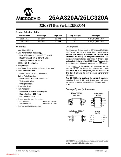
TSSOP/MSOP (ST, MS)
CS 1 SO 7 HOLD 6 SCK 5 SI
PDIP/SOIC
(P, SN)
CS 1 SO 2 WP 3 VSS 4
8 VCC 7 HOLD 6 SCK 5 SI
X-Rotated TSSOP (X/ST)
HOLD 1 VCC 2 CS 3 SO 4
† NOTICE: Stresses above those listed under “Absolute Maximum Ratings” may cause permanent damage to the device. This is a stress rating only and functional operation of the device at those or any other conditions above those indicated in the operational listings of this specification is not implied. Exposure to maximum rating conditions for an extended period of time may affect device reliability.
- Standby Current: 5 μA at 5.5V
• 4096 x 8-bit Organization
• 32-Byte Page
• Self-Timed Erase and Write Cycles (5 ms max.)
• Block Write Protection
- Protect none, 1/4, 1/2 or all of array
MBRB40250TG;中文规格书,Datasheet资料
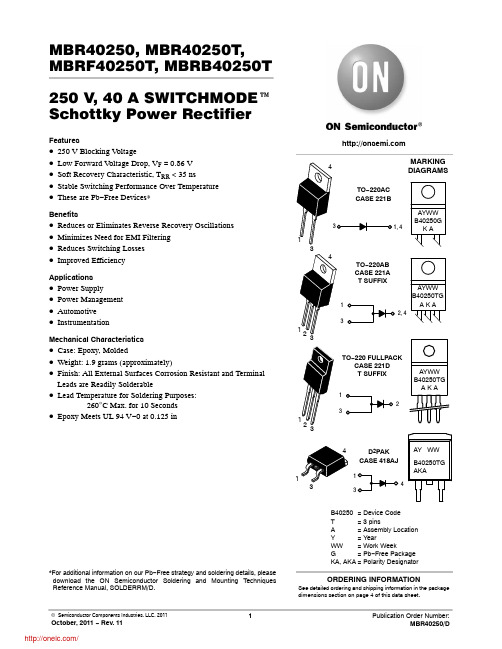
MBR40250, MBR40250T, MBRF40250T, MBRB40250T
TYPICAL CHARACTERISTICS
100
100
IF, MAXIMUM FORWARD CURRENT (A)
TJ = 150°C
TJ = 125°C 10
TJ = 100°C TJ = 25°C
TJ = 150°C
• Power Supply • Power Management • Automotive • Instrumentation
Mechanical Characteristics
• Case: Epoxy, Molded • Weight: 1.9 grams (approximately) • Finish: All External Surfaces Corrosion Resistant and Terminal
AKA
1 3
4
D2PAK
CASE 418AJ
1
4 3
AY WW
B40250TG AKA
*For additional information on our Pb−Free strategy and soldering details, please download the ON Semiconductor Soldering and Mounting Techniques Reference Manual, SOLDERRM/D.
Benefits
• Reduces or Eliminates Reverse Recovery Oscillations • Minimizes Need for EMI Filtering • Reduces Switching Losses • Improved Efficiency
FGA20N120FTDTU;中文规格书,Datasheet资料
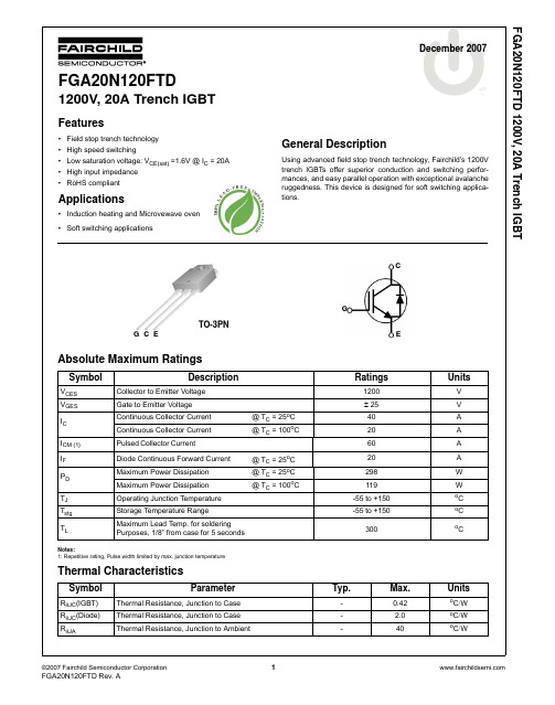
GCE
TO-3PN
Absolute Maximum Ratings
Symbol
VCES VGES IC
ICM (1) IF PD
TJ Tstg TL
Description
Collector to Emitter Voltage Gate to Emitter Voltage Continuous Collector Current Continuous Collector Current Pulsed Collector Current
oC
Typ.
-
Max.
0.42 2.0 40
Units
oC/W oC/W oC/W
FGA20N120FTD 1200V, 20A Trench IGBT
Package Marking and Ordering Information
Device Marking
©2007 Fairchild Semiconductor Corporation
1
FGA20N120FTD Rev. A
G
E
Ratings
1200 ± 25 40 20 60 20 298 119 -55 to +150 -55 to +150 300
Units
V V A A A A W W oC oC
Applications
• Induction heating and Microvewave oven • Soft switching applications
December 2007
tm
General Description
Using advanced field stop trench technology, Fairchild’s 1200V trench IGBTs offer superior conduction and switching performances, and easy parallel operation with exceptional avalanche ruggedness. This device is designed for soft switching applications.
- 1、下载文档前请自行甄别文档内容的完整性,平台不提供额外的编辑、内容补充、找答案等附加服务。
- 2、"仅部分预览"的文档,不可在线预览部分如存在完整性等问题,可反馈申请退款(可完整预览的文档不适用该条件!)。
- 3、如文档侵犯您的权益,请联系客服反馈,我们会尽快为您处理(人工客服工作时间:9:00-18:30)。
ZXTN25020DZ20V NPN high gain transistor in SOT89SummaryBV CEX > 100V BV CEO > 20V BV ECX > 6V I C(cont) = 6AV CE(sat) < 48mV @ 1A R CE(sat) = 30m ⍀P D = 2.4WComplementary part number ZXTP25020DZDescriptionPackaged in the SOT89 outline this new low saturation 20V NPN transistor offers extremely low on state losses making it ideal for use in DC-DC circuits and various driving and power management functionsFeatures• 6 Amps continuous current •Up to 15 Amps peak current •High current gain•Very low saturation voltages •100V forward blocking voltage •6V reverse blocking voltageApplications•Emergency lighting circuits •Motor driving •Camera strobe •Boost converters •Backlight inverters •MOSFET gate drivers •LED DrivingOrdering informationDevice marking1K8DeviceReel size (inches)Tape width (mm)Quantity per reel ZXTN25020DZTA7121000Absolute maximum ratingsThermal resistanceNOTES:(a)For a device surface mounted on 15mm x 15mm x 0.6mm FR4 PCB with high coverage of single sided 1oz copper, in still air conditions.(b)Mounted on 25mm x 25mm x 0.6mm FR4 PCB with high coverage of single sided 1oz copper, in still air conditions.(c)Mounted on 50mm x 50mm x 0.6mm FR4 PCB with high coverage of single sided 2oz copper, in still air conditions.(d)As (c) above measured at t<5 seconds.(e)Junction to case (collector tab. TypicalParameterSymbol Limit Unit Collector-Base voltageV CBO 100V Collector-Emitter voltage (forward blocking)V CEX 100V Collector-Emitter voltageV CEO 20V Emitter-Collector voltage (reverse blocking)V ECX 6V Emitter-Base voltageV EBO 7V Continuous Collector current (c)I C 6A Base current I B 1A Peak pulse currentI CM 15A Power dissipation at T A =25°C (a)Linear derating factorP D1.18.8W mW/°C Power dissipation at T A =25°C (b)Linear derating factorP D 1.814.4W mW/°C Power dissipation at T A =25°C (c)Linear derating factorP D 2.419.2W mW/°C Power dissipation at T A =25°C (d)Linear derating factorP D 4.4635.7W mW/°C Power dissipation at T C =25°C (e)Linear derating factorP D 19.2153W mW/°C Operating and storage temperature rangeT j , T stg -55 to 150°CParameterSymbol Limit Unit Junction to ambient (a)R ⍜JA 117°C/W Junction to ambient (b)R ⍜JA 68°C/W Junction to ambient (c)R ⍜JA 51°C/W Junction to ambient (d)R ⍜JA 28°C/W Junction to case (e)R ⍜JC7.95°C/WThermal characteristicsThermal characteristicsElectrical characteristics (at T amb = 25°C unless otherwise stated).ParameterSymbol Min.Typ.Max.Unit Conditions Collector-Base breakdown voltageBV CBO 100125V I C = 100μACollector-Emitter breakdown voltage (forward blocking)BV CEX 100120V I C = 100μA, R BE ≤ 1k Ω or -1V < V BE < 0.25V Collector-Emitter breakdown voltage BV CEO 2035V I C = 10mA (*)NOTES:(*)Measured under pulsed conditions. Pulse width ≤ 300µs; duty cycle ≤ 2%.Emitter-collector breakdown voltage (reverse blocking)BV ECX 68V I E = 100μA, R BC ≤ 1k Ω or 0.25V > V BC > -0.25V Emitter-Collector breakdown voltage (reverse blocking)BV ECO 5.0 6.0V I E = 100μA Emitter-Base breakdown voltageBV EBO 7.08.3V I E = 100μACollector-Base cut-off currentI CBO <1500.5nA μA V CB = 100VV CB = 100V , T amb =100°C Collector-Emitter cut-off currentI CEX 100nA V CE = 100V , R BE ≤ 1k Ω or -1V < V BE < 0.25V Emitter cut-off current I EBO <150nA V EB = -5.6V Collector-Emitter saturation voltageV CE(sat)40601001301002104875120180120270mV mV mV mV mV mV I C = 1A, I B = 100mA (*)I C = 1A, I B = 20mA (*)I C = 2A, I B = 40mA (*)I C = 2A, I B = 20mA (*)I C = 3A, I B = 300mA (*)I C = 6A, I B = 300mA (*)Base-Emitter saturation voltageV BE(sat)10001050mV I C = 6A, I B = 300mA (*)Base-Emitter turn-on voltageV BE(on)875950mVI C = 6A, V CE = 2V (*)Static forward current transfer ratioh FE3002505045036011015900I C = 10mA, V CE = 2V (*)I C = 2A, V CE = 2V (*) I C = 6A, V CE = 2V (*)I C = 15A, V CE = 2V (*)Transition frequency f T 215MHz I C = 50mA, V CE = 10V f = 100MHzInput capacitance C ibo 152pF V EB = 0.5V, f = 1MHz (*)Output capacitance C obo 16.525pF V CB = 10V, f = 1MHz (*)Delay time t d 67.7ns I C = 1A, V CC = 10V, I B1 = -I B2 = 10mA Rise time t r 72.2ns Storage time t s 361ns Fall timet f63.9nsPackage outline - SOT89DIM Millimeters Inches DIM Millimeters Inches Min Max Min Max Min Max Min MaxA 1.40 1.600.5500.630E 2.29 2.600.0900.102B0.440.560.0170.022E1 2.13 2.290.0840.090 B10.360.480.0140.019e 1.50 BSC0.059 BSC C0.350.440.0140.017e1 3.00 BSC0.118 BSCD 4.40 4.600.1730.181H 3.94 4.250.1550.167D1 1.52 1.830.0640.072L0.89 1.200.0350.047 Note: Controlling dimensions are in millimeters. Approximate dimensions are provided in inchesZetex sales offices EuropeZetex GmbHKustermann-park Balanstraße 59D-81541 München GermanyTelefon: (49) 89 45 49 49 0Fax: (49) 89 45 49 49 49europe.sales@AmericasZetex Inc700 Veterans Memorial Highway Hauppauge, NY 11788USATelephone: (1) 631 360 2222Fax: (1) 631 360 8222usa.sales@Asia PacificZetex (Asia Ltd)3701-04 Metroplaza Tower 1Hing Fong Road, Kwai Fong Hong KongTelephone: (852) 26100 611Fax: (852) 24250 494asia.sales@Corporate HeadquartersZetex Semiconductors plcZetex Technology Park, Chadderton Oldham, OL9 9LL United KingdomTelephone: (44) 161 622 4444Fax: (44) 161 622 4446hq@© 2008 Published by Zetex Semiconductors plcDefinitionsProduct changeZetex Semiconductors reserves the right to alter, without notice, specifications, design, price or conditions of supply of any product or service. Customers are solely responsible for obtaining the latest relevant information before placing orders.Applications disclaimerThe circuits in this design/application note are offered as design ideas. It is the responsibility of the user to ensure that the circuit is fit for the user’s application and meets with the user’s requirements. No representation or warranty is given and no liability whatsoever is assumed by Zetex with respect to the accuracy or use of such information, or infringement of patents or other intellectual property rights arising from such use or otherwise. Zetex does not assume any legal responsibility or will not be held legally liable (whether in contract,tort (including negligence), breach of statutory duty, restriction or otherwise) for any damages, loss of profit, business, contract,opportunity or consequential loss in the use of these circuit applications, under any circumstances.Life supportZetex products are specifically not authorized for use as critical components in life support devices or systems without the express written approval of the Chief Executive Officer of Zetex Semiconductors plc. As used herein:A. Life support devices or systems are devices or systems which:1.are intended to implant into the body or2.support or sustain life and whose failure to perform when properly used in accordance with instructions for use provided in the labeling can be reasonably expected to result in significant injury to the user.B. A critical component is any component in a life support device or system whose failure to perform can be reasonably expected tocause the failure of the life support device or to affect its safety or effectiveness.ReproductionThe product specifications contained in this publication are issued to provide outline information only which (unless agreed by the company in writing) may not be used, applied or reproduced for any purpose or form part of any order or contract or be regarded as a representation relating to the products or services concerned. Terms and ConditionsAll products are sold subjects to Zetex’ terms and conditions of sale, and this disclaimer (save in the event of a conflict between the two when the terms of the contract shall prevail) according to region, supplied at the time of order acknowledgement.For the latest information on technology, delivery terms and conditions and prices, please contact your nearest Zetex sales office.Quality of productZetex is an ISO 9001 and TS16949 certified semiconductor manufacturer.To ensure quality of service and products we strongly advise the purchase of parts directly from Zetex Semiconductors or one of our regionally authorized distributors. For a complete listing of authorized distributors please visit: /salesnetworkZetex Semiconductors does not warrant or accept any liability whatsoever in respect of any parts purchased through unauthorized sales channels.ESD (Electrostatic discharge)Semiconductor devices are susceptible to damage by ESD. Suitable precautions should be taken when handling and transporting devices.The possible damage to devices depends on the circumstances of the handling and transporting, and the nature of the device. The extent of damage can vary from immediate functional or parametric malfunction to degradation of function or performance in use over time.Devices suspected of being affected should be replaced.Green complianceZetex Semiconductors is committed to environmental excellence in all aspects of its operations which includes meeting or exceeding reg-ulatory requirements with respect to the use of hazardous substances. Numerous successful programs have been implemented to reduce the use of hazardous substances and/or emissions.All Zetex components are compliant with the RoHS directive, and through this it is supporting its customers in their compliance with WEEE and ELV directives.Product status key:“Preview”Future device intended for production at some point. Samples may be available “Active”Product status recommended for new designs “Last time buy (LTB)”Device will be discontinued and last time buy period and delivery is in effect “Not recommended for new designs”Device is still in production to support existing designs and production “Obsolete”Production has been discontinued Datasheet status key:“Draft version”This term denotes a very early datasheet version and contains highly provisional information, whichmay change in any manner without notice.“Provisional version”This term denotes a pre-release datasheet. It provides a clear indication of anticipated performance.However, changes to the test conditions and specifications may occur, at any time and without notice.“Issue”This term denotes an issued datasheet containing finalized specifications. However, changes tospecifications may occur, at any time and without notice.分销商库存信息: DIODESZXTN25020DZTA。