DM368电源设计_slvrav5
Allen-Bradley

安装说明原版说明书译文Hiperface-to-DSL 反馈整流器套件产品目录号 2198-H2DCK变更摘要在后盖板增加了 EAC 徽标。
关于反馈整流器套件本套件适用于 Allen-Bradley® 2090 系列电机反馈电缆,且配备 10 个 Hiperface 编码器信号的接线端子。
Hiperface 编码器信号被转换成兼容的数字伺服链路 (DSL) 反馈信号。
必须为 10 针整流器套件连接器接线,并在正确放置电缆屏蔽层和电缆护套的情况下组装连接器壳体。
准备电缆如要将反馈整流器套件用于现有 Bulletin 2090 电缆,需要进行一些准备工作,以确保电缆屏蔽层、导线长度和剥线长度正确无误。
准备反馈电缆时,请遵循以下说明:•将屏蔽层修剪平整,以免绞线造成相邻端子短路。
•测量导线长度,确保其足够长,以提供工作回路。
•在每根导线上将剥掉足够长的屏蔽层,以提供合适的剥线长度。
反馈电缆尺寸单位为 mm (in.)在电缆护套上的位置2罗克韦尔自动化出版物 2198-IN006D-ZH-P - 2019年10 月Hiperface-to-DSL 反馈整流器套件安装整流器套件按照以下步骤安装整流器套件。
1.拆下保护盖,将信号线连接至合适的端子,为每个连接端留出工作回路。
有关 10 针端子插脚引线,请参见第 第3 页 页的 连接器数据。
2.以 0.25 N•m (2.2 lb•in) 的最大扭矩,拧紧端子螺丝。
3.将屏蔽夹夹到 12 mm (0.5in.) 的裸露电缆屏蔽层上,以在屏蔽编织层和屏蔽夹之间实现高效搭接。
4.连接扎带 (随套件一起提供),以消除应力。
5.以 0.3 N•m (2.6 lb•in) 的最大扭矩,拧紧屏蔽夹螺丝。
6.更换保护盖,然后安装保护盖螺丝。
以 0.3 N•m (2.6 lb•in) 的最大扭矩,拧紧保护盖螺丝。
7.将 2 针 DSL 连接器插入驱动连接器,然后将安装支架安装到其中一个安装位置 (共 3 个) 上。
LT3686:降压型DC/DC转换器

L 3 9 :.MH 降 压型 DC DC 换 器 T 9 022 z / 转
Ln a 推 出 3 0 i r e 5 mA、6 V超低 静态 电流降压型 开关 0
L3 9 : T 9 1降压 型 DC DC 转 换 器 /
师能够优化效率 ,同时避开关键噪声敏感频段 。其 1 0引线 化效率 ,同时避开关键 噪声敏感频段 。其 1 0引线 3 mm x 3 mm F 一0( MSOP 封装结合高开 关频率 , mm x2 D N1 或 ) 3 F mm D N或耐热增强型 MS OP封装结合 高开关频率 ,允
可 保持外部 电感器和 电容器 的小 尺寸 ,从而 提供一个 占板 许使 用小 的外部 电感器 和 电容器 ,从 而可提供 一个 占板面
面积紧凑和高热效率的解决方案。 瞄圆圈
Li ear ww w.i arc n n 1 ne , or cn
积紧凑和高热效率的解决方案。 匿圈目 圜
不 同 ,L 2 4 T 9 0运用一个真正 4象限模拟乘法器 ,该乘法器
L3 8 T 6 6的 开 关频 率 从 3 0 H 0 k z到 25 z是 用 户可 产 生 5 的功率 测量准 确度和 3 的 电流 测量准 确度 ,从 .MH % %
T90 编程的 ,从 而使 设计 jJ ̄ , 够最大 限度地提 高效率 ,同时避 而 确保 电路板和系统 实现 最佳功率效率和 可靠性 。L 2 4 H i i
开关键 噪声敏感频段。L 3 8 T 6 6运用一种独特的设计 ,确保 适 合用于线 路卡和服 务器 、功率检 测断路器 、电源控制环
恒 定频 率 切换 。
路和多种测量应用 。
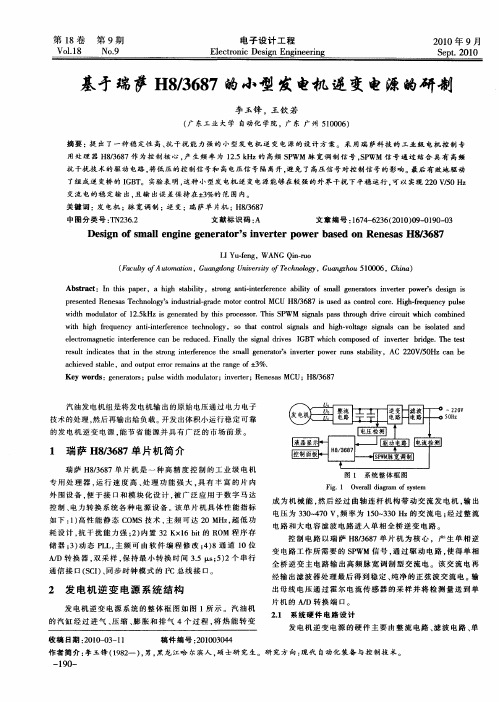
基矛瑞萨H8/3687的小型发电机逆变电源的研制
Vo .8 11 No9 .
电 子 设 计 工 程
E e to i e in En ie rn lcr nc D sg gn eig
21 0 0年 9月
S p .2 0 e t 01
基矛瑞萨 H8 67的小型 发电机 逆变电源的研制 /8 3
李玉锋 , 王钦 若
Ab t a t n ti a e , a h g t b l y s o g a t i tr r n e a i t f s l g n r tr n e tr p w r e in i sr c :I h s p p r i h sa i t , t n n i n e e e c bl y o ma l e e ao s i v re o e ' d sg s i r - f i s p e e td R n s sT c n lg ’ i d sr lg a e mo o o t lMC /6 7 i u e s c n rlc r . g -r q e c u s r s n e e e a e h oo yS n u t a —r d t rc n r U H8 8 s s d a o t o e Hih f u n y p l i o 3 o e e
e e t ma e i n e e e c a e r d c d F n l h i a rv s GB i h c mp s d o iv re b d e T e ts l cr o g t it r r n e c n b e u e . i al t e sg ld e I T wh c o o e f n et r r g . h e t n c f y n i i r s l id c t s t a n t e sr n n e e e c h mal g n r tr n e e o r r n tb l y,AC 2 0 / 0 a e e u t n ia e h t i h t g it r r n e t e s l e e ao ' i v r r p we u s s i t o f s t a i 2 V 5 Hz c n b a h e e t b e n u p t ro e i sa e r n e o ± % . c iv d sa l .a d o t u r rr man t h a g f 3 e t Ke r s e ea os u s i t d ltr n e e ;R n s s MCU;H8 3 8 y wo d :g n r tr ;p le w d h mo u ao ;iv r r e e a t ,6 7
DM368各个引脚

BGA ID NAME Type Group power supply Reset StateW1Vss GNDW2GIO32I/O/Z GIO /SPI2/VENCVDDS33InputW3GIO35I/O/Z GIO/SPI4/CLKOUTVDDS33InputW4GIO36I/O/Z GIO/SPI4/AEMIFVDDS33InputW5GIO41I/O/Z GIO/MMCSD/AEMIFVDDS33InputW6DDR_DQM1O DDR VDD18_DDR W7DDR_DQ12I/O DDR VDD18_DDR W8DDR_DQ8I/O DDR VDD18_DDR W9DDR_DQ6I/O DDR VDD18_DDR W10DDR_DQ4I/O DDR VDD18_DDR W11DDR_CLK O DDR VDD18_DDR W12~DDR_CLK O DDR VDD18_DDR W13~DDR_WE O DDR VDD18_DDRW14DDR_BA0O DDR VDD18_DDRW15DDR_A2O DDR VDD18_DDR W16DDR_A6O DDR VDD18_DDR W17DDR_A8O DDR VDD18_DDR W18DDR_A11O DDR VDD18_DDR W19Vss GNDV1GIO28I/O/Z GIO /SPI1/VENCVDDS33InputV2GIO23I/O/Z GIO/SPI0/PWM0VDDS33InputV3GIO33I/O/Z GIO /SPI2/USB/VENCVDDS33InputV4GIO34I/O/Z GIO /SPI2/USB/VENCVDDS33InputV5GIO38I/O/Z GIO/MMCSD1/AEMIFVDDS33InputV6DDR_DQ15I/O DDR VDD18_DDR V7DDR_DQ14I/O DDR VDD18_DDR V8DDR_DQ11I/O DDR VDD18_DDR V9DDR_DQ I/O DDR VDD18_DDR V10DDR_DQ3I/O DDR VDD18_DDR V11DDR_DQ1I/O DDR VDD18_DDR V12~DDR_CAS O DDR VDD18_DDRV13DDR_BA2O DDR VDD18_DDRV14DDR_A1O DDR VDD18_DDR V15DDR_A5O DDR VDD18_DDR V16DDR_A10O DDR VDD18_DDR V17DDR_A12O DDR VDD18_DDRV18EM_A13O AEMIF/GIO/BTSEL[2]VDD_AWMIF1_18_33InputV19EM_A11I/O/Z AEMIF/GIO/BTSEL[0]VDD_AWMIF1_18_33InputU1GIO26I/O/Z GIO /SPI1VDDS33InputU2GIO29I/O/Z GIO /SPI1/VENCVDDS33InputU3N.B.U4GIO31I/O/Z GIO /SPI2/CLKOUTVDDS33InputU5GIO40I/O/Z GIO/MMCSD1/AEMIFVDDS33InputU6DDR_DQSN1I/O DDR VDD18_DDRU7N.B.U8DDR_DQ9I/O DDR VDD18_DDRU9DDR_DQSN0I/O DDR VDD18_DDRU10N.B.U11DDR_DQ0I/O DDR VDD18_DDR U12~DDR_DQ0O DDR VDD18_DDR U13N.B.U14DDR_A0O DDR VDD18_DDR U15DDR_A4O DDR VDD18_DDR U16DDR_A9O DDR VDD18_DDR U17N.BU18EM_A12I/O/Z AEMIF/GIO/BTSEL[1]VDD_AWMIF1_18_33InputU19EM_A10I/O/Z AEMIF/GIO/BTSEL[2]VDD_AWMIF1_18_33InputT1GIO25I/O/Z GIO/SPI0/PWM1/UART1VDDS33InputT2GIO27I/O/Z GIO /SPI1/VENCVDDS33InputT3GIO24I/O/Z GIO /SPI0VDDS33InputT4GIO30I/O/Z GIO /SPI2/VENCVDDS33InputT5GIO37I/O/Z GIO/SPI4/MCBSP/CLKOUTVDDS33InputT6GIO43I/O/Z GIO/MMCSD1/AEMIFVDDS33InputT7DDR_DQS1I/O DDR VDD18_DDRT8DDR_DQGATE0O DDR VDD18_DDRT9DDR_DQGATE1I DDR VDD18_DDRT10DDR_DQS0I/O DDR VDD18_DDR T11DDR_DQM0O DDR VDD18_DDRT12~DDR_CS O DDR VDD18_DDR T13DDR_BA1O DDR VDD18_DDR T14DDR_A3O DDR VDD18_DDR T15DDR_A7O DDR VDD18_DDR T16DDR_A13O DDR VDD18_DDRT17EM_A7I/O/Z AEMIF/GIO/KEYSCANVDD_AWMIF1_18_33InputT18EM_A9I/O/Z AEMIF/GIO/BTSEL[1]VDD_AWMIF1_18_33InputT19EM_A8I/O/Z AEMIF/GIO/BTSEL[0]VDD_AWMIF1_18_33InputR1RSV1OR2GIO22I/O/Z GIO/SPI10VDDS33Input R3VPP PWRR4RSV2IR5GIO39I/O/Z GIO/MMCSD1/AEMIFVDDS33InputR6GIO42I/O/Z GIO/MMCSD1/AEMIFVDDS33InputR7DDR_DQ13I/O DDR VDD18_DDR R8DDR_DQ10I/O DDR VDD18_DDR R9DDR_DQ7I/O DDR VDD18_DDR R10DDR_DQ2I/O DDR VDD18_DDR R11DDR_PADREFP O DDR VDD18_DDR R12VDD18_DDR PWRR13DDR_CKE O DDR VDD18_DDR R14VDD_AEMIF1_18_33PWRR15EM_A3I/O/Z AEMIF/GIO/KEYSCANVDD_AWMIF1_18_33InputR16EM_A5I/O/Z AEMIF/GIO/KEYSCANVDD_AWMIF1_18_33InputR17EM_BA1I/O/Z AEMIF/GIO/KEYSCAN/HPIVDD_AWMIF1_18_33InputR18EM_A6I/O/Z AEMIF/GIO/KEYSCANVDD_AWMIF1_18_33InputR19EM_A4I/O/Z AEMIF/GIO/KEYSCANVDD_AWMIF1_18_33InputP1USB_DM A I/O USBPHY VDDA33_USB P2VSSA18_USB GNDP3VSSA33_USB GNDP4VDDA33_USB PWRP5VDDS33PWRP6VDDS33PWRP7VDDS18PWRP8VSS GNDP9VDD18_DDR PWRP10VDD18_DDR PWRP11DDR_VREF PWR DDR VDD18_DDR P12VDD18_DDR PWRP13VSS GNDP14VDD_AEMIF1_18_33PWRP15EM_D12I/O/Z AEMIF/GIO/HPIVDD_AWMIF1_18_33InputP16EM_D14I/O/Z AEMIF/GIO/HPIVDD_AWMIF1_18_33InputP17EM_BA0I/O/Z AEMIF/GIO/KEYSCANVDD_AWMIF1_18_33InputP18EM_D15I/O/Z AEMIF/GIO/HPIVDD_AWMIF1_18_33InputP19EM_D13I/O/Z AEMIF/GIO/HPIVDD_AWMIF1_18_33InputN1USB_DP A I/O USBPHY VDDA33_USB N2USB_VBUS A I/O USBPHY USB_VBUS N3N.B.N4VDDA18_PLL PWRN5VDD18_USB PWRN6VDDS33PWRN7N.B.N8VSS GNDN9VDD18_DDR PWRN10N.B.N11VDD18_DDR PWRN12VSS GNDN13N.B.N14VSS GNDN15EM_D8I/O/Z AEMIF/GIO/HPIVDD_AWMIF1_18_33InputN16EM_D11I/O/Z AEMIF/GIO/HPIVDD_AWMIF1_18_33InputN17N.B.N18EM_D10I/O/Z AEMIF/GIO/HPIVDD_AWMIF1_18_33InputN19EM_D9I/O/Z AEMIF/GIO/HPIVDD_AWMIF1_18_33InputM1USB_ID AI USBPHY VDDA33_USBM2PWRCNTON I PRTCSS VDD12_PRTCSS InputM3PWRST I PRTCSS VDD12_PRTCSS Input M4VSSA GNDM5VDDA12LDO_USB PWR OUTPUT M6CVDD PWRM7VSS GNDM8VSS GNDM9VSS GNDM10CVDD PWRM11VSS GNDM12CVDD PWRM13CVDD PWRM14VDDS18PWRM15EM_CLK I/O/Z AEMIF/GIO/HPIVDDS33OUTPUTM16EM_ADV I/O/Z AEMIF/GIO/HPIVDD_AWMIF1_18_33OUTPUTM17~EM_CE[0]I/O/Z AEMIF/GIO/HPIVDD_AWMIF1_18_33OUTPUTM18EM_A2I/O/Z AEMIF/HPI VDD_AWMIF2_18_33OUTPUT M19EM_A1I/O/Z AEMIF/HPI VDD_AWMIF2_18_33OUTPUT L1MXI1I CLOCKS VDDMXI InputL2VSS_MX1GNDL3PWCTRO3O PRTCSS VDD18_PRTCSS OL4PWCTRO2I/O/Z PRTCSS VDD18_PRTCSS OUTPUT L5PWCTRO1O PRTCSS VDD18_PRTCSS OUTPUT L6VDDMXI PWRL7VSS GNDL8VSS GNDL9VSS GNDL10VSS GNDL11VSS GNDL12VDDS33PWRL13CVDD PWRL14VDD_AEMIF2_18_33PWRL15EM_D4I/O/Z AEMIF/HPI VDD_AWMIF2_18_33Input L16EM_D7I/O/Z AEMIF/HPI VDD_AWMIF2_18_33InputL17EM_A0I/O/Z AEMIF/GIO/KEYSCAN/HPIVDD_AWMIF2_18_33InputL18EM_D6I/O/Z AEMIF/HPI VDD_AWMIF2_18_33Input L19EM_D5I/O/Z AEMIF/HPI VDD_AWMIF2_18_33Input k1MXO1O CLOCKS VDDMXI Inputk2PWCTRO0O PRTCSS VDD18_PRTCSS OUTPUT k3N.B.k4PWCTRIO6I/O/Z PRTCSS VDD18_PRTCSS Inputk5PWCTRIO5I/O/Z PRTCSS VDD18_PRTCSS Inputk6VDD18_PRTCSS PWRk7VDD12_PRTCSS PWRk8CVDD PWRk9VSS GNDk10VSS GNDk11VSS GNDk12CVDD PWRk13N.B.k14VDD_AEMIF2_18_33PWRk15EM_D3I/O/Z AEMIF/HPI VDD_AWMIF2_18_33Inputk16EM_D1I/O/Z AEMIF/GIO/HPIVDD_AWMIF2_18_33Inputk17N.B.k18EM_D0I/O/Z AEMIF/GIO/HPIVDD_AWMIF2_18_33Inputk19EM_D2I/O/Z AEMIF/HPI VDD_AWMIF2_18_33Input J1PWCTRIO2I/O/Z PRTCSS VDD18_PRTCSS InputJ2PWCTRIO1I/O/Z PRTCSS VDD18_PRTCSS Input J3PECTRIO0I/O/Z PRTCSS VDD18_PRTCSS Input J4PWCTRIO4I/O/Z PRTCSS VDD18_PRTCSS Input J5PWCTRIO3I/O/Z PRTCSS VDD18_PRTCSS InputJ6VDD12_PRTCSS PWRJ7VDDS18PWRJ8CVDD PWRJ9VSS GNDJ10VSS GNDJ11VSS GNDJ12CVDD PWRJ13VSS GNDJ14CVDD PWRJ15EM_WE I/O/Z AEMIF/GIO/HPIVDD_AWMIF2_18_33OUTPUTJ16MMCSD0_CLK O MMCSD0VDDS33OUTJ17~EM_CE[1]I/O/Z AEMIF/GIO/HPIVDD_AWMIF2_18_33OUTPUTJ18EM_WAIT I/O/Z AEMIF/GIO/HPIVDD_AWMIF2_18_33OUTPUTJ19EM_OE I/O/Z AEMIF/GIO/HPIVDD_AWMIF2_18_33InputH1RTCXO O PRTCSS VDD12_PRTCSS OUTPUT H2VSS_32K GNDH3~RESET I VDDS33InputH4EMU1I/O EMULATIONVDDS33InputH5~TRST I EMULATIONVDDS33InputH6VDDS33PWRH7CVDD PWRH8CVDD PWRH9VSS GNDH10VSS GNDH11VDDS18PWRH12CVDD PWRH13VDDS33PWRH14VDDS18PWRH15MMCSD0_CMD I/O/Z MMCSD0VDDS33Input H16MMCSD0_DATA3I/O/Z MMCSD0VDDS33Input H17MMCSD0_DATA2I/O/Z MMCSD0VDDS33Input H18MMCSD0_DATA0I/O/Z MMCSD0VDDS33Input H19MMCSD0_DATA1I/O/Z MMCSD0VDDS33Input G1RTCXI I PRTCSS VDD12_PRTCSS InputG2TMS I EMULATIONVDDS33InputG3N.B.G4TDO O EMULATIONVDDS33OUTPUTG5EMU0I/O EMULATIONVDDS33InputG6CVDD PWRG7N.B.G8CVDD PWRG9VDDA18_ADC PWRG10N.B.G11VSS GNDG12VSS GNDG13N.B.G14VDDS18PWRG15HSYNC I/O VENC/GIO VDDS33Input G16YOUT7I/O VENC VDDS33InputG17N.B.G18VSYNC I/O VENC/GIO VDDS33Input G19YOUT6I/O VENC VDDS33Input F1GIO20I/O/ZF2RTCK O EMULATIONVDDS33OUTPUTF3GIO21I/O/Z GIO/UART1/I2CVDDS33InputF4TCK I EMULATIONVDDS33InputF5TDI I EMULATIONVDDS33InputF6VDDS33PWR F7VDDS33PWRF8VSSA_ADC GNDF9VSSA18_VC GNDF10VDDS33PWRF11VSSA12_DAC GND VIDEO DACF12VDD_ISIF18_33PWRF13VDD_ISIF18_33PWRF14VSS GNDF15YOUT5I/O VENC VDDS33Input F16YOUT3I/O VENC VDDS33Input F17YOUT1I/O VENC VDDS33Input F18YOUT4I/O VENC VDDS33InputF19YOUT2I/O VENC VDDS33InputE1GIO16I/O/Z GIO /EMAC/UART1VDDS33InputE2GIO18I/O/Z GIO/UART0VDDS33InputE3GIO19I/O/Z GIO/UART0VDDS33InputE4GIO17I/O/Z GIO /EMAC/UART1VDDS33InputE5VDD18_SLDO PWRE6GPIO46I/O/Z GIO/Mcbsp VDDS33Input E7GIO44I/O/Z GIO/Mcbsp VDDS33InputE8ADC_CH0AI ADC VDD18_ADCE9VDDA18_VC PWRE10VDDA33_VC PWRE11VSSA18_DAC GND VIDEO DACE12VDDA12_DAC PWR VIDEO DAC VDDA12_DACE13C_WE_FIELD I/O ISIF/GIO/CLKOUT/USBVDD_ISIF18_33InputE14VSS GNDE15COUT5I/O GIO/VENC/PWEM2/RTOVDDS33InputE16YOUT0I/O VENC VDDS33InputE17COUT4I/O GIO/VENC/PWEM2/RTO1VDDS33InputE18COUT7I/O GIO/VENC/PWEM0VDDS33InputE19COUT6I/O GIO/VENC/PWEM1VDDS33InputD1GIO14I/O/Z GIO /EMAC VDDS33Input D2GIO15I/O/Z GIO /EMAC VDDS33Input D3GIO13I/O/Z GIO /EMAC VDDS33InputD4VDDRAM O OUTPUTD5GIO49I/O/Z GIO/Mcbsp VDDS33Input D6GIO1I/O/Z GIO /EMAC VDDS33InputD7ADC_CH4AI ADC VDD18_ADCD8ADC_CH3AI ADC VDD18_ADCD9VSSA33_VC GNDD10VDDA18_DAC PWR VIDEO DAC VDDA18_DACD11VREF AI VIDEO DAC VDDA18_DACD12YIN4I/O ISIF/GIO/SPI3VDD_ISIF18_33InputD13PCLK I/O/Z ISIF VDD_ISIF18_33Input D14YIN1I/O ISIF/GIO VDD_ISIF18_33Input D15YIN0I/O ISIF/GIO VDD_ISIF18_33InputD16COUT3I/O GIO/VENC/PWEM2/RTO2VDDS33InputD17COUT0I/O GIO/VENC/PWEM3VDDS33InputD18COUT1I/O GIO/VENC/PWEM3VDDS33InputD19COUT2I/O GIO/VENC/PWEM2/RTO3VDDS33InputC1GIO12I/O/Z GIO /EMAC VDDS33Input C2GIO9I/O/Z GIO /EMAC VDDS33Input C3N.B.C4GIO2I/O/Z GIO /EMAC VDDS33Input C5GIO3I/O/Z GIO /EMAC VDDS33Input C6GIO47I/O/Z GIO/Mcbsp VDDS33Input C7N.B.C8MICIN AI VCODEC VDDA33_VC orVDDA18_VCC9LINEO AO VCODEC VDDA33_VC orVDDA18_VCC10N.B.C11COMPPR AO VIDEO DAC VDDA18_DACC12YIN7I/O ISIF/GIO/SPI3VDD_ISIF18_33InputC13N.B.C14HD I/O ISIF/GIO VDD_ISIF18_33Input C15CIN6I/O ISIF VDD_ISIF18_33Input C16CIN2I/O ISIF VDD_ISIF18_33Input C17N.B.C18FIELD I/O GIO/VENC/PWEM3VDDS33InputC19LCD_OE I/O VENC/GIO VDDS33Input B1GIO11I/O/Z GIO /EMAC VDDS33Input B2GIO10I/O/Z GIO /EMAC VDDS33Input B3GIO6I/O/Z GIO /EMAC VDDS33Input B4GIO5I/O/Z GIO /EMAC VDDS33Input B5GIO0I/O/Z GIO VDDS33Input B6GPIO45I/O/Z GIO/Mcbsp VDDS33InputB7ADC_CH1AI ADC VDD18_ADCB8MICIP AI VCODEC VDDA33_VC orVDDA18_VCB9SPP AO VCODEC VDDA33_VC orVDDA18_VCB10VFB AI/O VIDEO DAC VDDA18_DAC B11IDACOUT AI/O VIDEO DAC VDDA18_DAC B12COMPY AO VIDEO DAC VDDA18_DACB13YIN5I/O ISIF/GIO/SPI3VDD_ISIF18_33InputB14VD I/O ISIF/GIO VDD_ISIF18_33Input B15YIN2I/O ISIF/GIO VDD_ISIF18_33Input B16CIN5I/O ISIF vDD_ISIF18_33Input B17CIN0I/O ISIF vDD_ISIF18_33Input B18VCLK I/O VENC/GIO VDDS33InputB19EXTCLKEXTCLK I/O GIO/VENC/PWEM3VDDS33InputA1RSV00A2GIO8I/O/Z GIO /EMAC VDDS33Input A3GIO7I/O/Z GIO /EMAC VDDS33InputA4GIO4I/O/Z GIO /EMAC VDDS33Input A5GIO48I/O/Z GIO/Mcbsp VDDS33InputA6ADC_CH5AI ADC VDD18_ADCA7ADC_CH2AI ADC VDD18_ADCA8VCOM AO VCODEC VDDA33_VC orVDDA18_VCA9SPN AO VCODEC VDDA33_VC orVDDA18_VCA10TVOUT AI/O VIDEO DAC VDDA18_DAC A11IREF AI/O VIDEO DAC VDDA18_DAC A12COMPPB AO VIDEO DAC VDDA18_DACA13YIN6I/O ISIF/GIO/SPI3VDD_ISIF18_33InputA14YIN3I/O ISIF/GIO VDD_ISIF18_33Input A15CIN7I/O ISIF VDD_ISIF18_33Input A16CIN4I/O ISIF VDD_ISIF18_33Input A17CIN3I/O ISIF VDD_ISIF18_33Input A18CIN1I/O ISIF VDD_ISIF18_33Input A19VSS GNDDescriptionDigital groundGIO: GIO[32]SPI2: ClockVENC: Red output data bit 0GIO: GIO[35]SPI4: Slave Out Master In dataSPI4: SPI4 Chip Select 1CLKOUT: Output Clock 1GIO: GIO[36]SPI4: ClockAsync EMIF: Address bit[21]Async EMIF: Address bit[14]GIO: GIO[41]MMCSD1: DATA3Async EMIF: Address bit[18]Data mask input for DDR_DQ[15:8]DDR Data Bus bit 12DDR Data Bus bit 08DDR Data Bus bit 06DDR Data Bus bit 04DDR Data ClockDDR Complementary Data ClockDDR Write EnableBank select outputs. Two are required for 1Gb DDR2 memories.DDR Address Bus bit 02DDR Address Bus bit 06DDR Address Bus bit 08DDR Address Bus bit 11Digital groundGIO: GIO[28]SPI1: ClockVENC: Blue output data bit 1GIO: GIO[23]SPI0: Slave Out Master In dataSPI0: SPI0 Chip Select 1PWM0: OutputGIO: GIO[33]SPI3: SPI3 Chip Select 0USB: USB: Digital output to control external 5 V supplyVENC: Red output data bit 1GIO: GIO[33]SPI3: SPI3 Chip Select 0USB: USB: Digital output to control external 5 V supplyVENC: Red output data bit 1GIO: GIO[38]MMCSD1: DATA0Async EMIF: Address bit[15]DDR Data Bus bit 15DDR Data Bus bit 14DDR Data Bus bit 11DDR Data Bus bit 05DDR Data Bus bit 03DDR Data Bus bit 01DDR Column Address StrobeBank select outputs. Two are required for 1Gb DDR2 memories.DDR Address Bus bit 01DDR Address Bus bit 05DDR Address Bus bit 10DDR Address Bus bit 12Async EMIF: Address Bus bit[13]GIO: GIO[78] BTSEL[2]: See Section 3.2, Device Boot Modes for system usage of these pins.Async EMIF: Address Bus bit[11]GIO: GIO[76] BTSEL[0]: See Section 3.2, Device Boot Modes for system usage of these pins.GIO: GIO[26]SPI1: Slave In Master Out dataGIO: GIO[29]SPI1: SPI1 Chip Select 0VENC: Green output data bit 0GIO: GIO[31]SPI2: Slave Out Master In dataSPI2: SPI2 Chip Select 1CLKOUT: Output Clock 2GIO: GIO[40]MMCSD1: DATA2Async EMIF: Address bit[17]DDR: Complimentary data strobe input/outputs for each byte of the 16-bit data bus. They are outputs to the DDR2 when writing and inputs when reading.They are used to synchronize the data transfers. Note: This signal is used in double ended differential memory interfaces supported by the device.DDR Data Bus bit 09DDR: Complimentary data strobe input/outputs for each byte of the 16-bit data bus. They are outputs to the DDR2 when writing and inputs when reading.They are used to synchronize the data transfers. Note: This signal is used in double ended differentialmemory interfaces supported by the device.DDR Data Bus bit 00DDR Row Address StrobeDDR Address Bus bit 00DDR Address Bus bit 04DDR Address Bus bit 09Async EMIF: Address Bus bit[12]GIO: GIO[77] BTSEL[1]: See Section 3.2, Device Boot Modes for system usage of these pins.Async EMIF: Address Busbit[10]GIO:GIO[75]AECFG[2]: See Section 3.2, Device Boot Modes and Table 3-14, AECFG (Async EMIF Configuration) forsystem usage of these pins.GIO: GIO[25]SPI0: SPI0 Chip Select 0PWM1: OutputUART1: Transmit dataGIO: GIO[27]SPI1: Slave Out Master In dataSPI1: SPI1 Chip Select 1VENC: Blue output data bit 1GIO: GIO[24]SPI0: ClockGIO: GIO[30]SPI2: Slave In Master Out dataVENC: Green output data bit 1GIO: GIO[37]SPI4: SPI4 Chip Select 0McBSP: CLKS pin to source an external clock CLKOUT: Output Clock 0GIO: GIO[43]MMCSD1: ClockAsync EMIF: Address bit[20]Data strobe input/outputs for each byte of the 16-bit data bus used to synchronize the data transfers.Output to DDR2 when writing and inputs when eading. They are used to synchronize the data ransfers.DDR_DQS1: For DDR_DQ[15:8]DDR: Loopback signal for external DQS gating. Route to DDR and back to DDR_DQGATE1 withsame constraints as used for DDR clock and data. DDR: Loopback signal for external DQS gating. Route to DDR and back to DDR_DQGATE0 withsame constraints as used for DDR clock and data. Data strobe input/outputs for each byte of the 16-bit data bus used to synchronize the data transfers.Output to DDR2 when writing and inputs when reading. They are used to synchronize the data transfers.DDR_DQS0: For DDR_DQ[7:0]Data mask input for DDR_DQ[7:0]DDR Chip SelectBank select outputs. Two are required for 1Gb DDR2 memories.DDR Address Bus bit 03DDR Address Bus bit 07DDR Address Bus bit 13Async EMIF: Address Bus bit[07]GIO: GIO[72]Keyscan: A3Async EMIF: Address Bus bit[09]GIO: GIO[74] AECFG[1]: See Section 3.2, Device Boot Modes and Table 3-14, AECFG (Async EMIF Configuration) for system usage of these pins.Async EMIF: Address Bus bit[08]GIO: GIO[73] AECFG[0]: See Section 3.2, Device Boot Modes and Table 3-14, AECFG (Async EMIF Configuration) for system usage of these pins. For proper device operation, this pin must be left unconnected.GIO: GIO[22]SPI0: Slave In Master Out dataFor proper device operation, this pin must always be connected to CVDD.For proper device operation, this pin must be tied to ground.GIO: GIO[39]MMCSD1: DATA1Async EMIF: Address bit[16]GIO: GIO[42]MMCSD1: CommandAsync EMIF: Address bit[19]DDR Data Bus bit 13DDR Data Bus bit 10DDR Data Bus bit 07DDR Data Bus bit 02DDR: External resistor ( 50 ohm to ground) Power supply for DDR (1.8 V).DDR Clock EnablePower supply for switchable AEMIF (3.3/1.8 V). VDD_AEMIF1_18_33: can be used as a power supply for EM_A[3:13], EM_BA0, EM_BA1, EM_CE[0],EM_ADV, EM_CLK, EM_D[8:15] or as GPIO pins.See AEMIF pin descriptions.VDD_AEMIF2_18_33:can be used as a power supply for EM_A[0:2], EM_CE[1], EM_WE, EM_OE, EM_WAIT, EM_D[0:7] pins, HPI, or GPIO pins. See AEMIF pin descriptions.Example 1: VDD_AEMIF2_18_33 at 1.8-V for 8-bit NAND VDD_AEMIF1_18_33at 3.3-V for GPIOExample 2: VDD_AEMIF1_18_33and VDD_AEMIF2_18_33 at 1.8-V for 16-bit NAND.Async EMIF: Address Bus bit[03]GIO: GIO[68]Keyscan: B3Async EMIF: Address Bus bit[05]GIO: GIO[70]Keyscan: A1Async EMIF: Bank Address 1 signal = 16-bit address.In 16-bit mode, lowest address bit.In 8-bit mode, second lowest address bitGIO: GIO[66]Keyscan: B1HPI: This pin is host interrupt output HINT Note: HPI is pin multiplexed with Asynchronous EMIF at the output pin. HPI is available only when boot mode selected is HPI boot mode. Inthis configuration, the device will always act as a slave.Async EMIF: Address Bus bit[06]GIO: GIO[71]Keyscan: A2Async EMIF: Address Bus bit[04]GIO: GIO[69]Keyscan: A0USB D- (differential signal pair)Note: If the USB peripheral is not used at all in the application, this pin should be connected to VSS.1.8-V USB groundNote: If the USB peripheral is not used at all in the application, this pin should be connected to VSS.3.3-V USB groundNote: If the USB peripheral is not used at all in the application, this pin should be connected to VSS.USB D- (differential signal pair)Note: If the USB peripheral is not used at all in the application, this pin should be connected to VSS.Power supply for 3.3-V I/O.Power supply for 3.3-V I/O.Power supply for 1.8-V I/O.Digital groundPower supply for DDR (1.8 V).Power supply for DDR (1.8 V).DDR: DDR_VREF is .5* VDD18_DDR= 0.9V for SSTL2 specific reference voltage.Power supply for DDR (1.8 V).Digital groundPower supply for switchable AEMIF (3.3/1.8 V). VDD_AEMIF1_18_33: can be used as a power supply for EM_A[3:13], EM_BA0, EM_BA1, EM_CE[0],EM_ADV, EM_CLK, EM_D[8:15] or as GPIO pins.See AEMIF pin descriptions.VDD_AEMIF2_18_33:can be used as a power supply for EM_A[0:2], EM_CE[1], EM_WE, EM_OE, EM_WAIT, EM_D[0:7] pins, HPI, or GPIO pins. See AEMIF pin descriptions.Example 1: VDD_AEMIF2_18_33 at 1.8-V for 8-bit NAND VDD_AEMIF1_18_33 at 3.3-V for GPIOExample 2: VDD_AEMIF1_18_33 and VDD_AEMIF2_18_33 at 1.8-V for 16-bit NAND.Async EMIF: Data Bus bit[12]GIO: GIO[61]HPI: Data bus bit [12]Note: HPI is pin multiplexed with Asynchronous EMIF at the output pin. HPI is available only when boot mode selected is HPI boot mode. Inthis configuration, the device will always act as a slave.Async EMIF: Data Bus bit[14]GIO: GIO[63]HPI: Data bus bit [14]Note: HPI is pin multiplexed with Asynchronous EMIF at the output pin. HPI is available only when boot mode selected is HPI boot mode. Inthis configuration, the device will always act as a slave.Async EMIF: Bank Address 0 signal = 8-bit address.In 8-bit mode, lowest address bit.Async EMIF: Address line (bit[14] when using 16-bitmemories.GIO: GIO[65]Keyscan: B0Async EMIF: Data Bus bit[15]GIO: GIO[64]HPI: Data bus bit [15]Note: HPI is pin multiplexed with Asynchronous EMIF at the output pin. HPI is available only when boot mode selected is HPI boot mode. Inthis configuration, the device will always act as a slave.GIO: GIO[62]HPI: Data bus bit [13]Note: HPI is pin multiplexed with Asynchronous EMIF at the output pin. HPI is available only when boot mode selected is HPI boot mode. Inthis configuration, the device will always act as a slave.USB D+ (differential signal pair)Note: If the USB peripheral is not used at all in the application, this pin should be connected to 3.3V .This pin is used by the USB Controller to detect a presence of 5V power (4.4V is the threshold) on the USB_VBUS line for normal operation. This power is sourced by the USB Component that is assuming the role of a Host. In other words, the power on the USB_VBUS line is not sourced by the Device. From DM368 perspective, when operating as a Host, it ensures that the external power supply that the DM368 has sourced is within the required voltage evel (>= 4.4V) and when DM368 is operating as a Device, the presence of a 5V power on the VBUS Line is used to signify the presence of an externalHost.Note 1: When the DM368 is operating as a Device, it uses the power on the USB_VBUS line to power up its internal pull-up resistor on the D+ line. Note2: If the USB peripheral is not used at all in the application, this pin should be connected to VSS.Analog power for PLL (1.8 V).1.8-V USB analog power supplyNote: If the USB peripheral is not used at all in the application, this pin should be connected to 1.8V.Power supply for 3.3-V I/O.Digital groundPower supply for DDR (1.8 V).Power supply for DDR (1.8 V).Digital groundDigital groundGIO: GIO[57]HPI: Data bus bit [8]Note: HPI is pin multiplexed with Asynchronous EMIF at the output pin. HPI is available only when boot mode selected is HPI boot mode. Inthisconfiguration, the device will always act as a slave.Async EMIF: Data Bus bit[11]GIO: GIO[60]HPI: Data bus bit [11]Note: HPI is pin multiplexed with Asynchronous EMIF at the output pin. HPI is available only when boot mode selected is HPI boot mode. Inthis configuration, the device will always act as a slave.Async EMIF: Data Bus bit[10]GIO: GIO[59]HPI: Data bus bit [10]Note: HPI is pin multiplexed with Asynchronous EMIF at the output pin. HPI is available only when boot mode selected is HPI boot mode. Inthis configuration, the device will always act as a slave.Async EMIF: Data Bus bit[09]GIO: GIO[58]HPI: Data bus bit [9]Note: HPI is pin multiplexed with Asynchronous EMIF at the output pin. HPI is available only when boot mode selected is HPI boot mode. Inthis configuration, the device will always act as a slave.USB operating mode identification pin.For device mode operation only, pull up this pin to VDD with a 1.5K ohm resistor.For host mode operation only, pull down this pin to ground (VSS) with a 1.5K ohm resistor.If using an OTG or mini-USB connector, this pin will be set properly via the cable/connector configurationNote: If the USB peripheral is not used at all in the application, this pin should be connected to 3.3V.PRTCSS: Reset pin for system power sequencing For more pin details, see Section 6.7.PRTCSS: Reset signal for PRTCSSFor more pin termination details, see Section 6.7,Power Management and Real Time Clock Subsystem (PRTCSS).Analog groundFor proper device operation, even if the USB peripheral is not used, a 0.22µF capacitor must be connected as close as possible to the package, and the capacitor mst be connected to V SSA.Core power (1.35-V).Digital groundDigital groundDigital groundCore power (1.35-V).Digital groundCore power (1.35-V).Core power (1.35-V).Power supply for 1.8-V I/O.Async EMIF: Clock signal for OneNAND flash interfaceGIO: GIO[50]Async EMIF: Address Valid Detect for OneNAND nterfaceGIO: GIO[51]HPI: This pin is host read or write select input.Async EMIF: Lowest numbered Chip Select. Can be programmed to be used for standard asynchronous memories (example:flash), OneNand or NAND memory. Used for the default boot and ROM boot modes.GIO: GIO[56]HPI: this pin is HPI chip select input.Note: HPI is pin multiplexed with Asynchronous EMIF at the output pin. HPI is available only when boot mode selected is HPI boot mode. Inthis configuration, the device will always act as a slave.Async EMIF: Address Bus bit[02]HPI: The state of HCNTLA and HCNTLB determines if address, data, or control information is being transmitted between an external host and the deviceNote: HPI is pin multiplexed with Asynchronous EMIF at the output pin. HPI is available only when boot mode selected is HPI boot mode. Inthis configuration, the device will always act as a slave.Async EMIF: Address Bus bit[01]HPI: This pin is half-word identification input HHWIL.Note: HPI is pin multiplexed with Asynchronous EMIF at the output pin. HPI is available only when boot mode selected is HPI boot mode. Inthis configuration, the device will always act as a slave.Crystal input for system oscillatorNote: If an external oscillator is to be used, the external oscillator clock signal should be connected to the MXI1 pin with a 1.8V amplitude. The MXO1 should be left unconnected and theVSS_MX1 signal should be connected to board ground (Vss).System oscillator - groundNote: Note: If an external oscillator is used, this pin must be connected to board ground (V ss).PRTCSS: General Output Signal 3For more pin termination details, see Section 6.7,Power Management and Real Time Clock Subsystem (PRTCSS).PRTCSS: General Output Signal 2For more pin termination details, see Section 6.7,Power Management and Real Time Clock Subsystem (PRTCSS).PRTCSS: General Output Signal 1For more pin termination details, see Section 6.7,Power Management and Real Time Clock Subsystem (PRTCSS).Power supply for PLL oscillator (1.8 V).Digital groundDigital groundDigital groundDigital groundDigital groundPower supply for 3.3-V I/O.Core power (1.35-V).Power supply for switchable AEMIF (3.3/1.8 V). VDD_AEMIF1_18_33: can be used as a power supply for EM_A[3:13], EM_BA0, EM_BA1, EM_CE[0],EM_ADV, EM_CLK, EM_D[8:15] or as GPIO pins.See AEMIF pin descriptions.VDD_AEMIF2_18_33:can be used as a power supply for EM_A[0:2], EM_CE[1], EM_WE, EM_OE, EM_WAIT, EM_D[0:7] pins, HPI, or GPIO pins. See AEMIF pin descriptions.Example 1: VDD_AEMIF2_18_33 at 1.8-V for 8-bit NAND VDD_AEMIF1_18_33at 3.3-V for GPIOExample 2: VDD_AEMIF1_18_33and VDD_AEMIF2_18_33 at 1.8-V for 16-bit NAND.Async EMIF: Data Bus bit[04]HPI: Data bus bit [4]Note: HPI is pin multiplexed with Asynchronous EMIF at the output pin. HPI is available only when boot mode selected is HPI boot mode. Inthis configuration, the device will always act as a slave.Async EMIF: Data Bus bit[07]HPI: Data bus bit [7]Note: HPI is pin multiplexed with Asynchronous EMIF at the output pin. HPI is available only when boot mode selected is HPI boot mode. Inthis configuration, the device will always act as a slave.Async EMIF: Address Bus bit[00] Note that the EM_A0 is always a 32-bit addressGIO: GIO[56]Keyscan: B2HPI: The state of HCNTLA and HCNTLB determines if address, data, or control information is being transmitted between an external host and the deviceNote: HPI is pin multiplexed with Asynchronous EMIF at the output pin. HPI is available only when boot mode selected is HPI boot mode. Inthis configuration, the device will always act as a slave.。
联盛德微电子 W0802P模块硬件设计指导书说明书

W0802P模块硬件设计指导书V7.1北京联盛德微电子有限责任公司 (winner micro)地址:北京市海淀区阜成路67号银都大厦6层电话:+86-10-62161900公司网址:文档历史北京联盛德微电子有限责任公司目录1概述 (1)2模块管脚定义 (1)3模块原理图设计 (3)4典型外围电路设计 (3)4.1电源供电 (3)4.2Reset电路设计 (4)4.3Wakeup电路设计 (4)4.4Boot下载功能 (4)4.5GPIO功能 (4)4.6ESD防护 (4)5模块外围设计 (4)5.1模块封装设计 (4)5.2模块布局设计 (5)5.3模块GPIO Layout设计 (6)6产品结构设计 (7)1概述W0802P是基于嵌入式Wi-Fi/蓝牙双模 SoC芯片W800设计的物联网无线模块。
该模块支持2.4G IEEE802.11 b/g/n Wi-Fi协议,内置完整的TCP/IP协议栈;支持蓝牙/BLE 4.2协议,支持蓝牙配网,支持蓝牙Mesh。
模块适用于智能家电、智能家居、无线音视频、智能玩具、医疗监护、工业控制、医疗监护等广泛的物联网领域,是物联网应用的理想解决方案。
W0802P采用SMD封装,邮票孔式接口,PCB板载天线。
可通过标准SMT设备实现产品的快速生产,为客户提供高可靠性的连接方式,特别适合自动化、大规模、低成本的现代化生产方式,方便应用于各种物联网硬件终端场合。
2模块管脚定义模块管脚排列及尺寸信息如图2-1所示:图2-1 模块引脚排列及尺寸图模块管脚说明如表2-1所示:表2-1 模块管脚说明3模块原理图设计44.1 电源供电建议模块电源输入脚至少放置一个47uF 滤波电容,且外部供电电源的最大输出电流建议在500mA 及以上。
CON1J24.2Reset电路设计模块上电自动复位,如果外部主控单元控制该管脚,低电平条件下模块复位。
4.3Wakeup电路设计Wakeup脚为外部唤醒脚,当芯片进入睡眠状态后,Wakeup脚给高电平时,芯片唤醒。
基于WT6632F的65WPD开关电源的设计

基于WT6632F的65WPD开关电源的设计基于WT6632F的65WPD开关电源的设计是一种用于为电子设备提供高效电力的电源设计。
WT6632F是一款具有多种保护功能的集成电路,适用于高效率隔离电源设计。
下面将从电源拓扑、功率转换、保护功能以及设计布局等方面,详细探讨基于WT6632F的65WPD开关电源的设计。
首先,根据65WPD的要求,可选取降压型稳压器作为电源拓扑,通过将输入交流电转换为直流电,并经过适当的电子元件和保护电路,实现输出稳压和过载保护。
其次,在功率转换方面,选择WT6632F集成电路作为控制主芯片,可通过其内部的PWM控制器来实现高效、可靠的电能转换。
该芯片内部具有一系列关键功能,包括过压保护、欠压保护、短路保护、过电流保护和过温保护等。
这些保护功能可以显著提高电源的稳定性和安全性。
然后,设计布局方面需要注意将输入和输出部分隔离,同时要防止高频噪音干扰。
可采用双层PCB设计,将输入部分和输出部分分开布局,并且通过适当的线路隔离和滤波电容来降低干扰。
此外,通过对输入滤波器的设计,可有效抑制开关电源输入端的高频噪音干扰,确保输入电流的纹波和噪音水平尽可能低。
同时,在输出端也需要合适的滤波电容和线路布局,以降低输出纹波和噪音,确保输出电流的稳定性和质量。
总之,基于WT6632F的65WPD开关电源的设计需要考虑电源拓扑、功率转换、保护功能和设计布局等多个方面。
只有在合理选择电源拓扑、充分利用WT6632F的保护功能、优化设计布局等条件下,才能实现高效、稳定、可靠的65WPD开关电源。
DC DC模块电源IB05_S-W75R3系列商品说明书
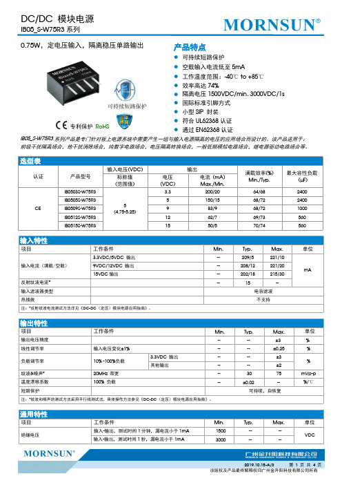
选型表认证产品型号输入电压(VDC)输出满载效率(%)Min./Typ.最大容性负载(µF)标称值(范围值)电压(VDC)电流(mA)Max./Min.CEIB0503S-W75R35(4.75-5.25)3.3200/2064/682400IB0505S-W75R35150/1568/722400IB0509S-W75R3983/968/721000IB0512S-W75R31262/769/73560IB0515S-W75R31550/570/74560输入特性项目工作条件Min.Typ.Max.单位输入电流(满载/空载)3.3VDC/5VDC 输出--209/5221/10mA9VDC/12VDC 输出--208/12221/2015VDC 输出--202/18215/30反射纹波电流*--15--输入滤波器类型电容滤波热插拔不支持注:*反射纹波电流测试方法详见《DC-DC (定压)模块电源应用指南》。
输出特性项目工作条件Min.Typ.Max.单位输出电压精度----±3%线性调节率输入电压变化±1%----±0.25%负载调节率10%-100%负载 3.3VDC 输出----±3%其他输出----±2纹波&噪声*20MHz 带宽--3075mVp-p 温度漂移系数100%负载--±0.02--%/℃短路保护可持续,自恢复注:*纹波和噪声的测试方法采用平行线测试法,具体操作方法参见《DC-DC (定压)模块电源应用指南》。
通用特性项目工作条件Min.Typ.Max.单位绝缘电压输入-输出,测试时间1分钟,漏电流小于1mA 1500----VDC输入-输出,测试时间1秒,漏电流小于1mA3000----0.75W ,定电压输入,隔离稳压单路输出专利保护RoHS产品特点●可持续短路保护●空载输入电流低至5mA ●工作温度范围:-40℃to +85℃●效率高达74%●隔离电压1500VDC/min,3000VDC/1s ●国际标准引脚方式●小型SIP 封装●符合UL62368认证●通过EN62368认证IB05_S-W75R3系列产品是专门针对板上电源系统中需要产生一组与输入电源隔离的电压的应用场合而设计的。
LM368

LM386中文资料是专为低损耗电源所设计的功率放大器集成电路。
它的内建增益为20,透过pin1和pin8脚位间电容的搭配,增益最高可达200。
LM386可使用电池为供应电源,输入电压范围可由4V~12V,无作动时仅消耗4mA电流,且失真低。
LM386的内部电路图及引脚排列图如图1、图2所示,表1为其电气特性。
图1.内部电路图图2引脚功能图极限参数:电源电压(LM386N-1,-3,LM386M-1)15V 电源电压(LM386N-4)22V封装耗散(LM386N)1.25W(LM386M)0.73W(LM386MM-1)0.595W输入电压±0.4V储存温度-65℃至+150℃操作温度0℃至+70℃结温+150℃焊接信息焊接(10秒)260℃小外形封装(SOIC和MSOP)气相(60秒)215℃红外(15秒)220℃热电阻qJC(DIP)37℃/WqJA(DIP)107℃/WqJC(SO封装)35℃/WqJA(SO封装)172℃/WqJA(MSOP封装)210℃/WqJC(MSOP封装)56℃/W表1.LM386电气特性Parameter参数测试条件OperatingSupplyVoltage(VS)操作电源电压-LM386N-1,-3,LM386M-1,LM386MM-14-12VLM386N-4-QuiescentCurrent(IQ)静态电流VS=6V,VIN=048mAOutputPower(POUT)输出功率--LM386N-1,LM386M-1,LM386MM-1VS=6V,RL=8W,THD=10%250325-mWLM386N-3VS=9V,RL=8W,THD=10%500700-mWLM386N-4VS=16V,RL=32W,THD=10%7001000-mWVS=6V,f=1kHz26-dB VoltageGain(AV)电压增益10μFfromPin1to846-d Bandwidth(BW)宽带VS=6V,Pins1and8Open300-kHzTotalHarmonicDistortion(THD)总谐波失真VS=6V,RL=8W,POUT=125 f=1kHz,Pins1and8OpenPowerSupplyRejectionRatio(PSRR)电源抑制比VS=6V,f=1kHz,CBYPASS Pins1and8Open,Referr OutputInputResistance(RIN)输入电阻--50-kΩInputBiasCurrent(IBIAS)输入偏置电流VS=6V,Pins2and3Open-250-nA图3的应用电路为增益20的情形,于pin1及pin8间加一个10 F的成200,如图4所示。
- 1、下载文档前请自行甄别文档内容的完整性,平台不提供额外的编辑、内容补充、找答案等附加服务。
- 2、"仅部分预览"的文档,不可在线预览部分如存在完整性等问题,可反馈申请退款(可完整预览的文档不适用该条件!)。
- 3、如文档侵犯您的权益,请联系客服反馈,我们会尽快为您处理(人工客服工作时间:9:00-18:30)。
IMPORTANT NOTICETexas Instruments Incorporated and its subsidiaries(TI)reserve the right to make corrections,modifications,enhancements,improvements, and other changes to its products and services at any time and to discontinue any product or service without notice.Customers should obtain the latest relevant information before placing orders and should verify that such information is current and complete.All products are sold subject to TI’s terms and conditions of sale supplied at the time of order acknowledgment.TI warrants performance of its hardware products to the specifications applicable at the time of sale in accordance with TI’s standard warranty.Testing and other quality control techniques are used to the extent TI deems necessary to support this warranty.Except where mandated by government requirements,testing of all parameters of each product is not necessarily performed.TI assumes no liability for applications assistance or customer product design.Customers are responsible for their products and applications using TI components.To minimize the risks associated with customer products and applications,customers should provide adequate design and operating safeguards.TI does not warrant or represent that any license,either express or implied,is granted under any TI patent right,copyright,mask work right, or other TI intellectual property right relating to any combination,machine,or process in which TI products or services are rmation published by TI regarding third-party products or services does not constitute a license from TI to use such products or services or a warranty or endorsement e of such information may require a license from a third party under the patents or other intellectual property of the third party,or a license from TI under the patents or other intellectual property of TI.Reproduction of TI information in TI data books or data sheets is permissible only if reproduction is without alteration and is accompanied by all associated warranties,conditions,limitations,and notices.Reproduction of this information with alteration is an unfair and deceptive business practice.TI is not responsible or liable for such altered rmation of third parties may be subject to additional restrictions.Resale of TI products or services with statements different from or beyond the parameters stated by TI for that product or service voids all express and any implied warranties for the associated TI product or service and is an unfair and deceptive business practice.TI is not responsible or liable for any such statements.TI products are not authorized for use in safety-critical applications(such as life support)where a failure of the TI product would reasonably be expected to cause severe personal injury or death,unless officers of the parties have executed an agreement specifically governing such use.Buyers represent that they have all necessary expertise in the safety and regulatory ramifications of their applications,and acknowledge and agree that they are solely responsible for all legal,regulatory and safety-related requirements concerning their products and any use of TI products in such safety-critical applications,notwithstanding any applications-related information or support that may be provided by TI.Further,Buyers must fully indemnify TI and its representatives against any damages arising out of the use of TI products in such safety-critical applications.TI products are neither designed nor intended for use in military/aerospace applications or environments unless the TI products are specifically designated by TI as military-grade or"enhanced plastic."Only products designated by TI as military-grade meet military specifications.Buyers acknowledge and agree that any such use of TI products which TI has not designated as military-grade is solely at the Buyer's risk,and that they are solely responsible for compliance with all legal and regulatory requirements in connection with such use. TI products are neither designed nor intended for use in automotive applications or environments unless the specific TI products are designated by TI as compliant with ISO/TS16949requirements.Buyers acknowledge and agree that,if they use any non-designated products in automotive applications,TI will not be responsible for any failure to meet such requirements.Following are URLs where you can obtain information on other Texas Instruments products and application solutions:Products ApplicationsAudio /audio Automotive and Transportation /automotiveAmplifiers Communications and Telecom /communicationsData Converters Computers and Peripherals /computersDLP®Products Consumer Electronics /consumer-appsDSP Energy and Lighting /energyClocks and Timers /clocks Industrial /industrialInterface Medical /medicalLogic Security /securityPower Mgmt Space,Avionics and Defense /space-avionics-defense Microcontrollers Video and Imaging /videoRFID OMAP Mobile Processors /omapWireless Connectivity /wirelessconnectivityTI E2E Community Home Page Mailing Address:Texas Instruments,Post Office Box655303,Dallas,Texas75265Copyright©2012,Texas Instruments Incorporated。