SPT601中文资料
PTS120660V010 PTC熔断器数据手册说明书

4397Product features• Positive Temperature Coefficient (PTC)• SMT resettable fuse • Low resistance • Fast time-to-trip• Voltage range 6 V to 60 V • Current range from 0.05A to 2.0A • 1206 (3216 metric) compact footprint •Moisture sensitivity level (MSL): 1Applications• USB peripherals•Plug and play protection for motherboards and peripherals • Power tools• Battery and port protection for mobile/smart phones • Game console port protection • Set-top-boxes•Tablets, notebooks, netbooks, laptops and desktops• Rechargeable battery packs •Digital cameras• Appliances and white goods •Consumer electronicsAgency information• cURus Recognition file number: E343021•TUV: R50192872PTS1206SMD PTC fusesPb HALOGENHF FREEEnvironmental compliancePart number/orderingPTS120660V010• PT= PTC fuse • S= Surface mount • 1206= size code•60V= Maximium dc voltage rating •010= Ihold rating (010=0.10 A2Technical Data 4397Effective November 2021PTS1206SMD PTC fuses/electronicsProduct specificationsVmax 1lmax 2lhold 3ltrip 4Pd 5Time to trip (maximum)Resistance Agency informationPart Number7(V dc )(A)(A)(A)typical (W)(A)(seconds)Initial (R i )minimum (Ω)1maximum (Ω)PartmarkingcURus TUVPTS120660V005601000.050.150.40.25 1.5 3.650TH x x PTS120660V010601000.100.250.40.5 1.0 1.615TY x x PTS120630V012301000.120.290.510.2 1.46TJ x x PTS120630V016301000.160.370.510.3 1.1 4.5TK x x PTS120624V020241000.200.420.680.10.65 2.6TL x x PTS120616V025161000.250.500.680.080.55 2.3TN x x PTS120616V035161000.350.750.680.10.25 1.2TP x x PTS12066V05061000.50 1.00.680.10.150.7TQ x x PTS120615V050151000.50 1.00.680.10.150.7TQ1x x PTS12066V07561000.75 1.50.680.10.090.29TR x x PTS12066V1006100 1.0 1.80.880.30.060.21TS x x PTS12066V1106100 1.1 2.20.880.10.070.2TU x x PTS12066V1506100 1.5 3.00.880.30.040.12TV x x PTS12066V20061002.03.51.081.50.020.08TXxxRecommended pad layout–mmDimensions–mm 1. Vmax: Maximum continuous voltage the device can withstand without damage at current 2. Imax: Maximum fault current the device can withstand without damage at rated voltage 3. Ihold: Maximum current the device will pass without interruption at +23 °C still air4.Itrip: Minimum current that will transition the device from low resistance to high resistance at +23 °C still air5. Pd: Power dissipated from the device when in tripped state at +23 °C still air6. R i : Minimum resistance of the device at +23 °CR 1: Maximum resistance of the device when measured one hour post reflow at +23 °C 7. Part Number Definition: PTS1206xVxxx PTS1206 = Product code and size xV = Voltage rating (Vmax) xxx = Ampere rating (Ihold)Part numberAminimum Amaximum Bminimum Bmaximum Cminimum Cmaximum Dminimum Dmaximum Eminimum EmaximumF G HPTS120660V005 3.00 3.50 1.50 1.800.500.900.1800.500.100.45 2.0 1.0 1.9PTS120660V010 3.00 3.50 1.50 1.800.500.900.1800.500.100.45 2.0 1.0 1.9PTS120630V012 3.00 3.50 1.50 1.800.350.680.1800.500.100.45 2.0 1.0 1.9PTS120630V016 3.00 3.50 1.50 1.800.280.680.1800.500.100.45 2.0 1.0 1.9PTS120624V020 3.00 3.50 1.50 1.800.280.680.1800.500.100.45 2.0 1.0 1.9PTS120616V025 3.00 3.50 1.50 1.800.280.680.1800.500.100.45 2.0 1.0 1.9PTS120616V035 3.00 3.50 1.50 1.800.280.680.1800.500.100.45 2.0 1.0 1.9PTS12066V050 3.00 3.50 1.50 1.800.280.680.1800.500.100.45 2.0 1.0 1.9PTS120615V050 3.00 3.50 1.50 1.800.28 1.060.1800.500.100.45 2.0 1.0 1.9PTS12066V075 3.00 3.50 1.50 1.800.280.680.1800.500.100.45 2.0 1.0 1.93Technical Data 4397Effective November 2021PTS1206SMD PTC fuses /electronicsTime to trip curves at +23ºCT emperature derating curve4Technical Data 4397Effective November 2021PTS1206SMD PTC fuses/electronicsGeneral specificationsOperating temperature: -40 °C to + 85 °C (with derating)Storage temperature: -10 °C to + 40 °C Storage relative humidity: 75%Storage conditon: Keep away form corrosive atmosphere and sunlight Storage duration: 1 yearThermal shock: (20 cycles - 40 °C to + 85 °C) -33% typical resistance change Humidity: +85 °C, 85% relative humidity, 1000 hours ±5% typical resistance change Resistance to solvents: MIL-STD- 202 Method 215Packaging information-mmSupplied in tape and reel packaging, 5000 parts per 7.0” diameter reel (EIA-481 compliant)PTS120630V012, PTS120630V016, PTS120624V020, PTS120616V025, PTS120616V035, PTS12066V050, PTS12066V075, PTS120660V005,PTS120660V010, PTS12066V100, PTS12066V110Section A–AUser Direction of FeedEatonElectronics Division 1000 Eaton Boulevard Cleveland, OH 44122United States/electronics© 2021 EatonAll Rights Reserved Printed in USAPublication No. 4397 PCN21026, PCN21027November 2021Technical Data 4397Effective November 2021PTS1206SMD PTC fuses Life Support Policy: Eaton does not authorize the use of any of its products for use in life support devices or systems without the express writtenapproval of an officer of the Company. Life support systems are devices which support or sustain life, and whose failure to perform, when properly used in accordance with instructions for use provided in the labeling, can be reasonably expected to result in significant injury to the user.Eaton reserves the right, without notice, to change design or construction of any products and to discontinue or limit distribution of any products. Eaton also reserves the right to change or update, without notice, any technical information contained in this bulletin.Solder reflow profileTable 1 - Standard SnPb solder (T c )Package thicknessVolume mm3 <350Volume mm3 ≥350<2.5 mm)235 °C 220 °C ≥2.5 mm220 °C220 °CTable 2 - Lead (Pb) free solder (T c )Package thicknessVolume mm 3 <350Volume mm 3350 - 2000Volume mm 3 >2000<1.6 mm 260 °C 260 °C 260 °C 1.6 – 2.5 mm 260 °C 250 °C 245 °C >2.5 mm250 °C245 °C245 °CT e m p e r a t u r eT LT PEaton is a registered trademark.All other trademarks are property of their respective owners.Follow us on social media to get the latest product and support information.Reference J-STD-020Profile featureStandard SnPb solderLead (Pb) free solderPreheat and soak • Temperature min. (T smin )100 °C 150 °C • Temperature max. (T smax )150 °C 200 °C • Time (T smin to T smax ) (t s )60-120 seconds 60-120 seconds Ramp up rate T L to T p3 °C/ second max. 3 °C/ second max.Liquidous temperature (T l ) Time (t L ) maintained above T L183 °C60-150 seconds 217 °C60-150 seconds Peak package body temperature (T P )*Table 1Table 2Time (t p )* within 5 °C of the specified classification temperature (T c )20 seconds*30 seconds*Ramp-down rate (T p to T L ) 6 °C/ second max. 6 °C/ second max.Time 25 °C to peak temperature6 minutes max.8 minutes max.* Tolerance for peak profile temperature (T p ) is defined as a supplier minimum and a user maximum.。
NC601系列产品说明书

北京浦特伟业科技有限公司 地 址:北京市昌平区黄平路 19 号院龙旗广场 2 号楼 816 室 电 话:82666020/88840664/8266055 传 真:010-82669890 EMAIL:sales@ 24 小时服务热线:13911070077
1
北京浦特伟业科技有限公司
目录
一.NC601 系列串口服务器简介 ..................................................................................................................... 4 1.1 概述 .................................................................................................................................................... 4 1.2 产品特性: ......................................................................................................................................... 5 1.3 硬件规格和尺寸: .............................................................................................................................. 5 1.4 硬件安装: ......................................................................................................................................... 6
SF-601说明书

继电保护信息送到继电保护装置及 9 号插件;另一路则作为收信电平显示、通道衰耗大号。 改变由 4 号插件送来的编码地址数据,可使 1 1 号插件中的收信输入滤波器中心频率自动切
换到所需的工作频率,并自动对其插件内部的增益进行控制,使每一个工作频率的收信灵敏启 动电平都调整在 4 . 0 d B m ,该编码地址数据还使 1 1 号插件中的收信衰耗器自动切换到预先设置好 的衰耗值,对每条线路的收信裕度进行单独调整。
贮存:-25℃ ̄+40℃。 3.6.2 相 对 湿 度
最湿月的月平均最大相对湿度为 9 0 % ,同时该月的月平均最低温度为 2 5 ℃且表面无凝露。最 高温度为 + 4 0 ℃时,平均最大相对湿度不超过 5 0 % 。 3.6.3 大气压力:80kPa ̄110kPa(海拔高度相当于 2000m 及以下)。
本装置“控制电路”( 9 号插件) 或继电保护装置送来的控制信号调制于载供电路送来的载波信号
上。正常运行时,该装置处于停信状态,不向通道发送高频信号。当输电线路发生故障时,继
电保护装置送来的启信或停信信号送入控制电路,使收发信机发信或停止发信,从而向通道传
送或停止传送高频信号。二是将已调制信号放大到所需要的功率电平值,经高频通道传送后,以
插件送来的高频信号,有效地解决因收发同频产生的差拍现象而导致收信解调输出信号失真问题。
收信回路的工作原理为超外差接收方式,传送到 1 1 号插件的高频信号经收信衰耗器与高频
接收带通滤波器选择后,送到混频器与由 8 号插件送来的本振信号( f + 1 2 k H z ) 混频,其输出信号 0
经“解调输出”( 1 0 号插件) 中的中频带通滤波器选出 1 2 k H z 中频信号。一路中频信号经解调得到
STSPIN32F0601电机评估板说明书

快速评估指南STSPIN32F0601电机评估板V1.3250w冰箱压缩机,泵类,风机和工业设备应用电机控制创新技术中心日程2简介3硬件和软件需求4电流采样电阻配置1主要日程5工作流程主要特征主要特征:•片上系统:STM32Cortex M0 +3相高压驱动•输入电压范围从35VAC(50VDC)到280VAC(400 VDC)•最大输入功率~300w•支持2+1采样电阻或者单电阻采样拓扑•Smart shutdown过流保护•SWD,UART和隔离的PWM输入信号接口STGD5H60DF x2STGD5H60DF x2STGD5H60DF x22+1电阻电流采样&过流检测IsSTSPIN32F0601SDVIPER122+15VLD1117S33TR+3.3VorSTCH02TR+15VSTD6N65M2+3.3VLD1117S33TR压缩机/风机/泵类电机简介•这个评估板是基于STSPIN32F0601片上系统的一个完整的3相电机驱动器,片上系统集成了3相600V 门极驱动器和Cortex®-M0 STM32MCU内核.•功率级包含了STGD5H60DF IGBT,也可以替换成其他同样是DPAK封装的IGBT或者MOSFET.•这个评估板同时支持2+1电阻电流采样和单电阻电流采样拓扑的无感磁场定向控制(FOC)的算法.•可以驱动永磁同步电机(PMSM)和无刷直流电机(BLDC).•它可以给不同应用领域的设备,包括冰箱压缩机,泵类,风机和其他工业设备提供一个易用性的整体方案.•这个评估板兼容宽范围的输入电压,还包括一个基于VIPER122的BUCK降压电路,来产生应用所需要的驱动电压+15V和3.3V电压•软件调试和配置可以通过标准的STM32工具软件和单独的STLINK调试器实现,预留了SWD和UART TX RX通讯接口.•隔离的PWM输入捕捉接口.硬件和软件需求使用STSPIN32F0601评估板对软件和硬件环境有以下的需求:•一台安装了windows(XP,Vista,Win7 ,Win8,Win10 )的个人电脑来安装软件包•一个隔离的ST-LINK/V2(v4.0.0或者更新)的调试器来连接STSPIN32F0601板到个人电脑•一个隔离的USB转UART转接线来连接STSPIN32F0601板到个人电脑(选配)•STM32电机控制软件开发包(MCSDK v5.3或更新)(官网下载)•STM32CubeMX(v4.24.0或更新)•一个兼容评估板额定电压和额定电流的3相PMSM电机或BLDC电机•交流电源供电或者直流电源供电•支持的IDE:–IAR Embedded Workbench® for Arm®(v7.80.4 or later)–Keil® MDK tools (v5.24.2 or later)–Ac6 System Workbench (v2.3.0 or later)关于正确安装介绍的单独的使用手册STMicroelectronics官方文档可以从ST官网获得:•STM32 motor control SDK v5.x tools user manual(UM2380)•STM32CubeMX for STM32 configuration and initialization C code generation user manual(UM1718)•STM32 ST-LINK utility software description user manual(UM0892)电流采样电阻配置•当SR1=0Ω,SR2=0Ω时,是单电阻采样模式--SR3为电流采样电阻•可以通过改变SR1=0.1Ω和SR2=0.1Ω来配置成2+ 1电阻模式--SR1:U相电流采样的电阻--SR2:V相电流采样的电阻--SR3:过流保护用的电阻•由于标准的MCSDK库无法支持2电阻采样拓扑,请在尝试2电阻模式前联系ST电机控制创新技术中心Motor Control Tuning GUI Motor Control WorkbenchProject ConfigurationCubeMX &IDESystemConfigurationGUIMotor ControlWorkbenchHW SetupFinalApplicationDevelopmentMCSDK工作流程第1步:填写电机参数•保存如下案例workbench文件<STSPIN32F0601_ST_board_1shunt_IARv7.stmcx>到你的工作目录下,然后通过ST Motor Control Workbench v5.4.3来打开它•改变参数为正在使用的电机参数•改变启动参数点击工程生成的图标,可以根据你选择的IDE环境来生成相应的工程STM32CubeMX被MC Workbench后台调用,用来生成适合所选择的IDE的工程框架当工程代码生成开始,将会显示进度条窗口显示用户脚本正在运行,当完成的时候,提示串口将会显示信息如下,用户信息将会更新打开工程文件编译和下载第4步:电机控制和监控通过隔离的UART连接评估板到你的个人电脑,然后开始尝试运行电机和实时监控电机运行状态11© STMicroelectronics -All rights reserved.ST logo is a trademark or a registered trademark of STMicroelectronics International NV or its affiliates in the EU and/or other countries. For additional information about ST trademarks, please refer to /trademarks.All other product or service names are the property of their respective owners.。
一种新式钢管的X射线检测系统

150研究与探索Research and Exploration ·智能检测与诊断中国设备工程 2020.08 (上)传统X 射线检测胶片损耗高,效率低本设计能够对φ25~φ102mm 范围直焊缝钢管不同管径进行缺陷的检测,该系统具有结构功能多、移动定位精度高、智能性高、适用性强及高效率等优点。
采用《固定式和移动式工业X 射线探伤机》《电离辐射防护与辐射源安全基本标准》《工业X 射线探伤放射卫生防护标准》《500kV 以下工业X 射线探伤机防护规则》《机电产品包装通用技术条件》最新国家相关标准进行设计,使无损检测设备的设计符合系列化、通用化、模块化和标准化等原则,以满足对设备快速、灵敏、精确和适应恶劣环境条件下的检测工作需要。
1 设备总体技术指标(1)适用检测范围:直径φ25~φ102mm;壁厚2mm,长度6.2m。
(2)检测速度:2~4m/min 可调;系统静态灵敏度:2.0%。
(3)图像质量:满足《工业X 射线图像增强器电视系统技术条件JBT 5453-2004》的要求。
(4)X 射线探伤机容量:160kV,10mA;X 射线探伤机频率:40kHz。
(5)最大穿透能力(标准工业拍片法):29mm Fe;工业电视最大穿透:20mm Fe。
(6)冷却方式:采用封闭式循环,强制风冷却油方式,外设温度显示,连续工作。
1.1 高频X 射线机系统X 射线机主要配置如图1、表1所示。
2 机械方案概述机械设备由160KV 射线机、6寸图像增强器铅房、钢管输送线组成。
整套方案为完成外径φ25~一种新式钢管的X 射线检测系统张欢1 ,田冰2 (1.亚泰集团丹东交通水泥有限公司,辽宁 丹东 118000;2.沈阳工业大学,辽宁 沈阳 110000)摘要:被检测钢管通过铅房钢管输送线沿X 向进入铅房,钢管的焊缝经过射线源与图像增强器进行检测,被检测的钢管通过钢管输送线输出铅房。
通过调整旋转滚的间距,使得设备能适应φ25mm-φ102mm 范围直焊缝钢管检测。
ADCMP600_601_602芯片手册

Rail-to-Rail, Very Fast, 2.5 V to 5.5 V,FEATURESFully specified rail to rail at V CC = 2.5 V to 5.5 VInput common-mode voltage from −0.2 V to VCC+ 0.2 V Low glitch CMOS-/TTL-compatible output stage3.5 ns propagation delay10 mW at 3.3 VShutdown pinSingle-pin control for programmable hysteresis and latch Power supply rejection > 50 dBImproved replacement for MAX999−40°C to +125°C operationAPPLICATIONSHigh speed instrumentationClock and data signal restorationLogic level shifting or translationPulse spectroscopyHigh speed line receiversThreshold detectionPeak and zero-crossing detectorsHigh speed trigger circuitryPulse-width modulatorsCurrent/voltage-controlled oscillatorsAutomatic test equipment (ATE)FUNCTIONAL BLOCK DIAGRAMNONINVERTINGINPUTINVERTINGINPUT(EXCEPT ADCMP600)Q OUTPUTDN(ADCMP602 ONLY)5914-1Figure 1.GENERAL DESCRIPTIONThe ADCMP600, ADCMP601, and ADCMP602 are very fast comparators fabricated on XFCB2, an Analog Devices, Inc. proprietary process. These comparators are exceptionally versatile and easy to use. Features include an input range from GND − 0.5 V to V CC + 0.2 V, low noise, TTL-/CMOS-compatible output drivers, and latch inputs with adjustable hysteresisand/or shutdown inputs.The device offers 5 ns propagation delay with 10 mV overdrive on 3 mA typical supply current.A flexible power supply scheme allows the devices to operate with a single +2.5 V positive supply and a −0.5 V to +2.8 V input signal range up to a +5.5 V positive supply with a −0.5 V to +5.8 V input signal range. Split input/output supplies with no sequencing restrictions on the ADCMP602 support a wide input signal range while still allowing independent output swing control and power savings.The TTL-/CMOS-compatible output stage is designed to drive up to 5 pF with full timing specs and to degrade in a graceful and linear fashion as additional capacitance is added. The comparator input stage offers robust protection against large input overdrive, and the outputs do not phase reverse when the valid input signal range is exceeded. Latch and programmable hysteresis features are also provided with a unique single-pin control option.The ADCMP600 is available in 5-lead SC70 and SOT-23 packages, the ADCMP601 is available in a 6-lead SC70 package, and the ADCMP602 is available in an 8-lead MSOP package.Rev. AInformation furnished by Analog Devices is believed to be accurate and reliable. However, noresponsibility is assumed by Analog Devices for its use, nor for any infringements of patents or other rights of third parties that may result from its use. Specifications subject to change without notice. No license is granted by implication or otherwise under any patent or patent rights of Analog Devices. T rademarks and registered trademarks are the property of their respective owners. One Technology Way, P.O. Box 9106, Norwood, MA 02062-9106, U.S.A. Tel: 781.329.4700 Fax: 781.461.3113 ©2006–2011 Analog Devices, Inc. All rights reserved.Rev. A | Page 2 of 16TABLE OF CONTENTSFeatures .............................................................................................. 1 Applications ....................................................................................... 1 Functional Block Diagram .............................................................. 1 General Description ......................................................................... 1 Revision History ............................................................................... 2 Specifications ..................................................................................... 3 Electrical Characteristics ............................................................. 3 Timing Information ......................................................................... 5 Absolute Maximum Ratings ............................................................ 6 Thermal Resistance ...................................................................... 6 ESD Caution .................................................................................. 6 Pin Configuration and Function Descriptions ............................. 7 Typical Performance Characteristics ............................................. 8 Application Information ................................................................ 10 Power/Ground Layout and Bypassing ..................................... 10 TTL-/CMOS-Compatible Output Stage ................................. 10 Using/Disabling the Latch Feature ........................................... 10 Optimizing Performance ........................................................... 11 Comparator Propagation Delay Dispersion ........................... 11 Comparator Hysteresis .............................................................. 11 Crossover Bias Point .................................................................. 12 Minimum Input Slew Rate Requirement ................................ 12 Typical Application Circuits ......................................................... 13 Outline Dimensions ....................................................................... 14 Ordering Guide .. (16)REVISION HISTORY1/11—Rev. 0 to Rev. AChanged V EE Pin to GND ............................................. ThroughoutChanges to Common-Mode Dispersion Conditions................... 4 Changes to Figure 15 and Figure 16 ............................................... 9 Changes to Comparator Hysteresis Section ................................ 12 Updated Outline Dimensions ....................................................... 14 Changes to Ordering Guide .......................................................... 15 10/06—Revision 0: Initial VersionSPECIFICATIONSELECTRICAL CHARACTERISTICSV CCI = V CCO = 2.5 V, T A = 25°C, unless otherwise noted.Rev. A | Page 3 of 16Rev. A | Page 4 of 161V IN = 100 mV square input at 50 MHz, V CM = 0 V, CL = 5 pF, V CCI = V CCO =2.5 V, unless otherwise noted.Rev. A | Page 5 of 16TIMING INFORMATIONFigure 2 illustrates the ADCMP600/ADCMP601/ADCMP602 latch timing relationships. Table 2 provides definitions of the terms shown in Figure 2.1.1V50%V N ± V OSDIFFERENTIAL INPUT VOLTAGELATCH ENABLEQ OUTPUT05914-025Figure 2. System Timing DiagramRev. A | Page 6 of 16ABSOLUTE MAXIMUM RATINGSStresses above those listed under Absolute Maximum Ratings may cause permanent damage to the device. This is a stress rating only; functional operation of the device at these or any other conditions above those indicated in the operationalsection of this specification is not implied. Exposure to absolute maximum rating conditions for extended periods may affect device reliability.THERMAL RESISTANCEθJA is specified for the worst-case conditions, that is, a device soldered in a circuit board for surface-mount packages.Rev. A | Page 7 of 16PIN CONFIGURATION AND FUNCTION DESCRIPTIONSQV P GND CCI /V CCON05914-002Q GND V P V CCI /V CCOLE/HYSV N05914-003V CCIV P V N S DN V CCO Q GNDLE/HYS05914-004Figure 3. ADCMP600 Pin Configuration Figure 4. ADCMP601 Pin ConfigurationFigure 5. ADCMP602 Pin ConfigurationRev. A | Page 8 of 16TYPICAL PERFORMANCE CHARACTERISTICSV CCI = V CCO = 2.5 V , T A = 25°C, unless otherwise noted.–800–11234567–600–400–200020040060080005914-007C U R R EN T (µA )LE/HYS (V)Figure 6. LE/HYS Pin I/V Characteristics 150–150–100–5050100–11023547605914-027C U R R E N T (µA )SHUTDOWN PIN VOLTAGE (V)Figure 7. S DN Pin I/V Characteristics05914-005I B (µA )COMMON-MODE VOLTAGE (V)–20–1515–1010–55020Figure 8. Input Bias Current vs. Input Common Mode 20–550–1010–1515–20–1.0–0.20.20.6–0.6 1.0 1.4 1.8 2.2 2.6 3.0 3.409514-011L O A D C U R R E N T (m A )V OUT (V)Figure 9. V OH /V OL vs. Current Load0501502504503505506505010015020025005914-008H Y S T E R E S I S (m V )HYSTERESIS RESISTOR (k Ω)Figure 10. Hysteresis vs. R HYS Control Resistor4500501001502002503003504000–5–10–15–2005914-026H Y S T E R E S I S (m V )PIN CURRENT (µA)Figure 11. Hysteresis vs. Pin CurrentRev. A | Page 9 of 164.83.03.23.43.63.84.04.24.44.610203040506070809010011012013014005914-009P R O P A G A T I O N D E L A Y (n s )OVERDRIVE (mV)Figure 12. Propagation Delay vs. Input Overdrive at V CC = 2.5 V4.03.83.43.63.23.0–0.600.6 1.2 1.8 2.4 3.005914-028P R O P A G A T I O N D E L A Y (n s )COMMON-MODE VOLTAGE (V)Figure 13. Propagation Delay vs. Input Common-Mode Voltageat V CC = 2.5 V5.03.03.23.43.63.84.04.24.44.64.82.53.03.54.06.05.55.04.505914-029P R O P A G A T I O N D E L A Y (n s )V CCO (V)RISEFALLFigure 14. Propagation Delay vs. V CCO05914-0121.00V/DIV M4.00nsFigure 15. 50 MHz Output Waveform V CC= 5.5 V05914-013500mV/DIV M4.00nsFigure16. 50 MHz Output Waveforms @ 2.5 VRev. A | Page 10 of 16APPLICATION INFORMATIONPOWER/GROUND LAYOUT AND BYPASSINGThe ADCMP600/ADCMP601/ADCMP602 comparators are very high speed devices. Despite the low noise output stage, it is essential to use proper high speed design techniques to achieve the specified performance. Because comparators are uncompensated amplifiers, feedback in any phase relationship is likely to cause oscillations or undesired hysteresis. Of critical importance is the use of low impedance supply planes, particularly the output supply plane (V CCO ) and the ground plane (GND). Individual supply planes are recommended as part of a multilayer board. Providing the lowest inductance return path for switching currents ensures the best possible performance in the target application.It is also important to adequately bypass the input and output supplies. Multiple high quality 0.01 µF bypass capacitors should be placed as close as possible to each of the V CCI and V CCO supply pins and should be connected to the GND plane with redundant vias. At least one of these should be placed to provide a physically short return path for output currents flowing back from ground to the V CC pin. High frequency bypass capacitors should be carefully selected for minimum inductance and ESR. Parasitic layout inductance should also be strictly controlled to maximize the effectiveness of the bypass at high frequencies.If the package allows and the input and output supplies have been connected separately such that V CCI ≠ V CCO , care should be taken to bypass each of these supplies separately to the GND plane. A bypass capacitor should never be connected between them. It is recommended that the GND plane separate the V CCI and V CCO planes when the circuit board layout is designed to minimize coupling between the two supplies and to take advantage of the additional bypass capacitance from each respective supply to the ground plane. This enhances the performance when split input/output supplies are used. If the input and output supplies are connected together for single-supply operation such that V CCI = V CCO , coupling between the two supplies is unavoidable; however, careful board placement can help keep output return currents away from the inputs.TTL-/CMOS-COMPATIBLE OUTPUT STAGESpecified propagation delay performance can be achieved only by keeping the capacitive load at or below the specified minimums. The outputs of the devices are designed to directly drive one Schottky TTL or three low power Schottky TTL loads or the equivalent. For large fan outputs, buses, or transmission lines, use an appropriate buffer to maintain the excellent speed and stability of the comparator.With the rated 5 pF load capacitance applied, more than half of the total device propagation delay is output stage slew time, even at 2.5 V V CC . Because of this, the total prop delay decreases as V CCO decreases, and instability in the power supply may appear as excess delay dispersion.This delay is measured to the 50% point for the supply in use; therefore, the fastest times are observed with the V CC supply at 2.5 V , and larger values are observed when driving loads that switch at other levels.When duty cycle accuracy is critical, the logic being driven should switch at 50% of V CC and load capacitance should be minimized. When in doubt, it is best to power V CCO or the entire device from the logic supply and rely on the input PSRR and CMRR to reject noise.Overdrive and input slew rate dispersions are not significantly affected by output loading and V CC variations.The TTL-/CMOS-compatible output stage is shown in the simplified schematic diagram (Figure 17). Because of its inherent symmetry and generally good behavior, this output stage is readily adaptable for driving various filters and otherunusual loads.05914-014Figure 17. Simplified Schematic Diagram of TTL-/CMOS-Compatible Output StageUSING/DISABLING THE LATCH FEATUREThe latch input is designed for maximum versatility. It can safely be left floating for fixed hysteresis or be tied to V CC to remove the hysteresis, or it can be driven low by any standard TTL/CMOS device as a high speed latch.In addition, the pin can be operated as a hysteresis control pin with a bias voltage of 1.25 V nominal and an input resistance of approximately 7000 Ω. This allows the comparator hysteresis to be easily and accurately controlled by either a resistor or an inexpensive CMOS DAC.Hysteresis control and latch mode can be used together if an open drain, an open collector, or a three-state driver is connected parallel to the hysteresis control resistor or current source. Due to the programmable hysteresis feature, the logic threshold of the latch pin is approximately 1.1 V regardless of V CC .ADCMP600/ADCMP601/ADCMP602OPTIMIZING PERFORMANCEAs with any high speed comparator, proper design and layout techniques are essential for obtaining the specified performance. Stray capacitance, inductance, inductive power and ground impedances, or other layout issues can severely limit performance and often cause oscillation. Large discontinuities along input and output transmission lines can also limit the specified pulse-width dispersion performance. The source impedance should be minimized as much as is practicable. High source impedance, in combination with the parasitic input capacitance of the comparator, causes an undesirable degradation in bandwidth at the input, thus degrading the overall response. Thermal noise from large resistances can easily cause extra jitter with slowly slewing input signals; higher impedances encourage undesired coupling.COMPARATOR PROPAGATION DELAY DISPERSIONThe ADCMP600/ADCMP601/ADCMP602 comparators are designed to reduce propagation delay dispersion over a wide input overdrive range. Propagation delay dispersion is thevariation in propagation delay that results from a change in the degree of overdrive or slew rate (that is, how far or how fast the input signal exceeds the switching threshold).Propagation delay dispersion is a specification that becomes important in high speed, time-critical applications, such as data communication, automatic test and measurement, and instru-mentation. It is also important in event-driven applications, suchas pulse spectroscopy, nuclear instrumentation, and medical imaging. Dispersion is defined as the variation in propagation delay as the input overdrive conditions are changed (Figure 18 and Figure 19).The device dispersion is typically < 2 ns as the overdrive varies from 10 mV to 125 mV . This specification applies to both positive and negative signals because the device has very closelymatched delays both positive-going and negative-going inputs.05914-015Figure 18. Propagation Delay—Overdrive Dispersion05914-016Figure 19. Propagation Delay—Slew Rate DispersionCOMPARATOR HYSTERESISThe addition of hysteresis to a comparator is often desirable in a noisy environment, or when the differential input amplitudes are relatively small or slow moving. Figure 20 shows the transfer function for a comparator with hysteresis. As the input voltage approaches the threshold (0.0 V , in this example) from below the threshold region in a positive direction, the comparator switches from low to high when the input crosses +V H /2, and the new switching threshold becomes −V H /2. The comparator remains in the high state until the new threshold, −V H /2, is crossed from below the threshold region in a negative direction. In this manner, noise or feedback output signals centered on 0.0 V input cannot cause the comparator to switch states unless it exceeds the region bounded by ±V H /2.05914-017Figure 20. Comparator Hysteresis Transfer FunctionThe customary technique for introducing hysteresis into a comparator uses positive feedback from the output back to the input. One limitation of this approach is that the amount of hysteresis varies with the output logic levels, resulting in hysteresis that is not symmetric about the threshold. The external feedback network can also introduce significant parasitics that reduce high speed performance and induce oscillation in some cases.These ADCMP600 features a fixed hysteresis of approximately 2 mV . The ADCMP601 and ADCMP602 comparators offer a programmable Hysteresis feature that can significantly improve accuracy and stability. Connecting an external pull-down resistor or a current source from the LE/HYS pin to GND, varies the amount of hysteresis in a predictable, stable manner.Leaving the LE/HYS pin disconnected results in a fixed hysteresis of 2 mV; driving this pin high removes hysteresis. The maximum hysteresis that can be applied using this pin is approximately 160 mV. Figure 21 illustrates the amount of hysteresis applied as a function of the external resistor value, and Figure 11 illustrates hysteresis as a function of the current. The hysteresis control pin appears as a 1.25 V bias voltage seen through a series resistance of 7 kΩ. The bias voltage changes± 20% throughout the hysteresis control range. The advantages of applying hysteresis in this manner are improved accuracy, improved stability, reduced component count, and maximumversatility. An external bypass capacitor is not recommended on the HYS pin because it impairs the latch function and often degrades the jitter performance of the device. As described in the Using/Disabling the Latch Feature section, hysteresis control need not compromise the latch function. CROSSOVER BIAS POINTIn both op amps and comparators, rail-to-rail inputs of this type have a dual front-end design. Certain devices are active near the V CC rail and others are active near the GND rail. At some predeter-mined point in the common-mode range, a crossover occurs. At this point, normally V CC/2, the direction of the bias current reverses and the measured offset voltages and currents change.The ADCMP600/ADCMP601/ADCMP602 comparators slightly elaborate on this scheme. Crossover points can be found at approximately 0.8 V and 1.6 V.50150250450350550650 501001502002505914-30 HYSTERESIS(mV)HYSTERESIS RESISTOR (kΩ)Figure 21. Hysteresis vs. R HYS Control Resistor MINIMUM INPUT SLEW RATE REQUIREMENTWith the rated load capacitance and normal good PC Board design practice, as discussed in the Optimizing Performance section, these comparators should be stable at any input slew rate with no hysteresis. Broadband noise from the input stage is observed in place of the violent chattering seen with most other high speed comparators. With additional capacitive loading or poor bypassing, oscillation is observed. This oscillation is due to the high gain bandwidth of the comparator in combination with feedback parasitics in the package and PC board. In many applications, chattering is not harmful.TYPICAL APPLICATION CIRCUITS05914-019Figure 22. Self-Biased, 50% SlicerDD05914-020Figure 23. LVDS-to-CMOS ReceiverCONTROL VOLTAGE 0V TO 2.5V05914-021Figure 24. Voltage-Controlled OscillatorINPUT 1.25V REFINPUT 1.25V ±50mV05914-022Figure 25. Oscillator and Pulse-Width Modulator05914-023Figure 26. Hysteresis Adjustment with LatchOUTLINE DIMENSIONSCOMPLIANT TO JEDEC STANDARDS MO-203-AA072809-A0.100.10Figure 27. 5-Lead Thin Shrink Small Outline Transistor Package (SC70)(KS-5)Dimensions shown in millimetersCOMPLIANT TO JEDEC STANDARDS MO-178-AA1.301.150.150.050.200.08MIN11-01-2010-AFigure 28. 5-Lead Small Outline Transistor Package (SOT-23)(RJ-5)Dimensions shown in millimetersCOMPLIANT TO JEDEC STANDARDS MO-203-AB072809-A0.100.10Figure 29. 6-Lead Thin Shrink Small Outline Transistor Package (SC70)(KS-6)Dimensions shown in millimetersCOMPLIANT TO JEDEC STANDARDS MO-187-AA0.800.550.400.100.950.8510-07-2009-BFigure 30. 8-Lead Mini Small Outline Package (MSOP)(RM-8)Dimensions shown in millimetersADCMP600/ADCMP601/ADCMP602ORDERING GUIDEModel 1 Temperature Range Package Description Package OptionBrandingADCMP600BRJZ-R2 −40°C to +125°C 5-Lead SO T23 RJ-5 G0C ADCMP600BRJZ-RL−40°C to +125°C 5-Lead SO T 23 RJ-5 G0C ADCMP600BRJZ-REEL7 −40°C to +125°C 5-Lead SO T 23 RJ-5 G0C ADCMP600BKSZ-R2 −40°C to +125°C 5-Lead SC70 KS-5 G0C ADCMP600BKSZ-RL −40°C to +125°C 5-Lead SC70 KS-5 G0C ADCMP600BKSZ-REEL7 −40°C to +125°C 5-Lead SC70 KS-5 G0C ADCMP601BKSZ-R2 −40°C to +125°C 6-Lead SC70 KS-6 G0N ADCMP601BKSZ-RL −40°C to +125°C 6-Lead SC70 KS-6 G0N ADCMP601BKSZ-REEL7 −40°C to +125°C 6-Lead SC70 KS-6 G0N ADCMP602BRMZ −40°C to +125°C 8-Lead MSOP RM-8GFADCMP602BRMZ-REEL −40°C to +125°C 8-Lead MSOP RM-8 GF ADCMP602BRMZ-REEL7 −40°C to +125°C 8-Lead MSOP RM-8GFEVAL-ADCMP600BRJZ Evaluation Board EVAL-ADCMP600BKSZ Evaluation Board EVAL-ADCMP601BKSZ Evaluation Board EVAL-ADCMP602BRMZ Evaluation Board1Z = RoHS Compliant Part.©2006–2011 Analog Devices, Inc. All rights reserved. Trademarks and registered trademarks are the property of their respective owners. D05914-0-1/11(A)。
罗氏 E 601 电化学发光免疫分析仪用户操作手册(中文)
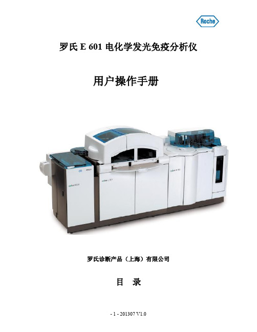
罗氏E 601 电化学发光免疫分析仪用户操作手册罗氏诊断产品(上海)有限公司目录第一章系统概述1、控制单元......................................................................... .. (3)2、核心单元......................................................................... (4)3、cobas e601免疫分析模块..................................................... .. . .. (5)第二章软件系统简介1、系统状态概览......................................................................... .. (12)2、日常工作菜单......................................................................... .. (13)第三章常规操作1、开机......................................................................... ................ .. (15)2、仪器准备......................................................................... . (16)3、增加新项目......................................................................... . (18)4、增加校准品........................................... ........ ...... .... ... ..... ..... (23)5、增加质控品 ........................................... ........ ...... .... ... ..... ..... (25)6、校准和质控检测 (30)7、样本检测 ........................................... ........ ...... .... ... ..... ..... ... .... .. 388、关机 ........................................... ........ ...... .... ... ..... ..... ... .... .. .... .. 44第四章维护保养1、每日保养......................................................................... . (46)2、每周保养......................................................................... .. (46)3、每两周保养......................................................................... . (48)4、每季保养......................................................................... . (49)5、按需保养......................................................................... . (49)第六章仪器报警信息......................................................................... .. 51第一章系统概述1、控制单元A 显示器(连接cobas link) D 触摸式显示器(主机)B 键盘/鼠标(连接cobas link) E 键盘/鼠标(主机)C 计算机(连接cobas link) F 计算机(主机)G 人体学PC支架2、核心单元1)核心单元轨道A 核心单元 E 模块轨道B 急诊标本位 F 常规标本上机位C 条形码阅读器G 标本退出位D 标本架转盘急诊标本位A 标本架托盘B 标本架C 标本杯、微量杯2)标本架及标本容器标本架不同类型、颜色和相应编号如下:标本容器有三种类型:标本试管、标本杯、校准及质控小瓶标本试管直径为13mm或16mm,长度为75mm或100mm;标本杯可插入16 mm标本试管中用。
GKP601 微机保护使用手册

4.30 定时限Ix过流保护 .................................................................. 33
4.31 反时限Ix过流保护 .................................................................. 33 4.32 非电量保护 .......................................................................... 34
3 操 作 说 明 ..................................................................................... 07 3.1 上电 ....................................................................................... 07 3.2 面板操作 ................................................................................. 07 3.3 显示内容说明 ........................................................................... 09 3.3.1 一次测量数据 ................................................................. 09 3.3.2 二次测量数据 ................................................................. 10 3.3.3 电度量数据 .................................................................... 10 3.3.4 开关量状态 .................................................................... 10 3.3.5 事件记录 ....................................................................... 10 3.3.6 保护定值查看 ................................................................. 11 3.3.7 设备参数 ....................................................................... 11 3.3.8 自检信息 ....................................................................... 12 3.3.9 时间查看 ........................................................................ 12 3.3.10 参数设置(出厂口令为2222) ............................................... 12
- 1、下载文档前请自行甄别文档内容的完整性,平台不提供额外的编辑、内容补充、找答案等附加服务。
- 2、"仅部分预览"的文档,不可在线预览部分如存在完整性等问题,可反馈申请退款(可完整预览的文档不适用该条件!)。
- 3、如文档侵犯您的权益,请联系客服反馈,我们会尽快为您处理(人工客服工作时间:9:00-18:30)。
V
6
Total Package Power
mW
500
Dissipation
Surge Current Rating
A
10
*The values indicated are absolute stress ratings. Functional operation of the device is not implied at these or any conditions in excess of those defined in electrical characteristics section of this document. Exposure to Absolute Ratings may cause permanent damage to the device and may adversely affect reliability.
Isolation Voltage -H Suffix
Isolation Resistance Coupled Capacitance
UNIT
V V mA µA pF
V V mA A µA V µA V µA µA µA
V V GΩ pF
MIN TYP MAX TEST CONDITIONS
1.2
1.5 If = 10mA
6
12
Ir = 10uA
2.5
5 Io = 400mA, resistive load
10 Vr = 6.0V
5
Vf = 0V
400
RGK = 10KΩ, TA = 100ºC, Id = 150µA
400
RGK=10KΩ, TA=100ºC, Id=150µA
400 If = 5mA
10 T = 16us
Forward Blocking Voltage Reverse Blocking Voltage Continuous Load Current Surge Current Rating Holding Current On-Voltage Leakage Current Gate Trigger Voltage Forward Leakage Current Reverse Leakage Current Gate Trigger Current COUPLED SPECIFICATIONS
OPTIONS/SUFFIXES*
• -H High Input-Output Isolation (5.3kVrms) • -S Surface Mount Leadform Option • -TR Tape and Reel Option
NOTE: Suffixes listed above are not included in marking on device for part number identification.
元器件交易网
SPT601
DC Input PhotoSCR
DESCRIPTION
The SPT601 consists of an AlGaAs LED optically coupled to a photo-sensitive SCR. Optical coupling provides high isolation levels while maintaining low-level DC signal control capability. With high load voltage and low input current, the SPT601 is an ideal solution to drive SCR Triacs and Solid State Relays.
APPROVALS
• UL, C-UL Pending
© 2004 Solid State Optronics • San José, CA • +1.408.293.4600
Page 1 of 5
SPT601 rev 1.40 (10/25/2004)
元器件交易网
SPT601
DC Input PhotoSCR
DISCLAIMER
Solid State Optronics (SSO) makes no warranties or representations with regards to the completeness and accuracy of this document. SSO reserves the right to make changes to product description, specifications at any time without further notice. SSO shall not assume any liability arising out of the application or use of any product or circuit described herein. Neither circuit patent licenses nor indemnity are expressed or implied. Except as specified in SSO's Standard Terms & Conditions, SSO disclaims liability for consequential or other damage, and we make no other warranty, expressed or implied, including merchantability and fitness for particular use.
BOTTOM VIEW/ BOARD PATTERN
© 2004 Solid State Optronics • San José, CA • +1.408.293.4600
Page 4 of 5
SPT601 rev 1.40 (10/25/2004)
元器件交易网
SPT601
DC Input PhotoSCR
ELECTRICAL CHARACTERISTICS - 25°C
PARAMETER
INPUT SPECIFICATIONS
LED Forward Voltage LED Reverse Voltage Must Operate Current Reverse Current Junction Capacitance OUTPUT SPECIFICATIONS
SCHEMATIC DIAGRAM
APPLICATIONS
• Valve control • Solenoids • Remote switching • Home appliances • Metering equipment • Heating elements
ABSOLUTE MAXIMUM RATINGS*
LIFE SUPPORT POLICY
SSO does not authorize use of its devices in life support applications wherein failure or malfunction of a device may lead to personal injury or death. Users of SSO devices in life support applications assume all risks of such use and agree to indemnify SSO against any and all damages resulting from such use. Life support devices are defined as devices or systems which, (a) are intended for surgical implant into the body, or (b) support or sustain life, and (c) whose failure to perform when used properly in accordance with instructions for use can be reasonably expected to result in significant injury to the user, or (d) a critical component in any component of a life support device or system whose failure can be reasonably expected to cause failure of the life support device or system, or to affect its safety or effectiveness.
Blocking Voltage (V)
© 2004 Solid State Optronics • San José, CA • +1.408.293.4600
Page 3 of 5
SPT601 rev 1.40 (10/25/2004)
元器件交易网
-40 -20 0
20 40 60 80
Tem perature (C)
SPT601
DC Input PhotoSCR
SPT601 Typical Blocking Voltage Distribution N = 100, Ambient Temperature = 25°C 60 50 40 30 20 10 0 425 450 475 500 525 550 575 600
20
50 VFX=100V, RRG=27KΩ, RL=10KΩ