SR05.TCT中文资料
2SCR553PT100;中文规格书,Datasheet资料

COLLECTOR SATURATION VOLTAGE : VCE(sat)[V]
1
Ta=25°C
1
IC/IB=20
10000
VCE=2V
COLLECTOR CURRENT : IC [mA]
1000
0.1
0.1
100
Ta=125°C 75°C 25°C -40°C
0.01
IC/IB=50 20 10
1 0.1
1
10
100
10 10
100 EMITTER CURRENT : IE[mA] Fig.8 Gain Bandwidth Product vs. Emitter Current
1000
100
COLLECTOR - BASE VOLTAGE : VCB [V] EMITTER - BASE VOLTAGE : VEB [V] Fig.7 Emitter Input Capacitance vs. Emitter-Base Voltage Collector Output Capacitance vs. Collector-Base Voltage
0.001 1 10 100 1000 10000 COLLECTOR CURRENT : IC[mA] Fig.5 Collector-Emitter Saturation Voltage vs. Collector Current ( ΙΙ )
1 0 0.5 1 1.5 BASE TO EMITTER VOLTAGE : VBE[V] Fig.6 Ground Emitter Propagation Characteristics
*1 Pw=10ms, Single Pulse *2 Each terminal mounted on a recommended land. *3 Mounted on a ceramic board. (40x40x0.7mm³)
RClamp0504S.TCT中文资料
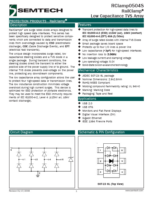
RailClamps are surge rated diode arrays designed to protect high speed data interfaces. This series has been specifically designed to protect sensitive components which are connected to data and transmission lines from overvoltage caused by ESD (electrostatic discharge), CDE (Cable Discharge Events), and EFT (electrical fast transients). The unique design incorporates surge rated, low capacitance steering diodes and a TVS diode in a single package. During transient conditions, the steering diodes direct the transient to either the positive side of the power supply line or to ground. The internal TVS diode prevents over-voltage on the power line, protecting any downstream components. The low capacitance array configuration allows the user to protect four high-speed data or transmission lines. The low inductance construction minimizes voltage overshoot during high current surges. This device is optimized for ESD protection of portable electronics. They may be used to meet the ESD immunity requirements of IEC 61000-4-2, Level 4 (±15kV air, ±8kV contact discharge).
SR540资料

SR520 – SR5605.0A SCHOTTKY BARRIER RECTIFIERSingle Phase, half wave, 60Hz, resistive or inductive load.For capacitive load, derate current by 20%.Characteristic Symbol SR520 SR530 SR540 SR550 SR560 UnitPeak Repetitive Reverse VoltageWorking Peak Reverse Voltage DC Blocking Voltage V RRMV RWM V R 2030405060V RMS Reverse VoltageV R(RMS)1421283542V Average Rectified Output Current (Note 1) @T L = 100°C I O 5.0A Non-Repetitive Peak Forward Surge Current 8.3ms Single half sine-wave superimposed on rated load (JEDEC Method)I FSM 150A Forward Voltage @I F = 5.0A V FM 0.550.70V Peak Reverse Current @T A = 25°C At Rated DC Blocking Voltage @T A = 100°C I RM 0.550mA Typical Junction Capacitance (Note 2)C j 550400pF Typical Thermal Resistance Junction to Ambient R JA 10K/W Operating and Storage Temperature RangeT j , T STG-65 to +150°CNote: 1. Valid provided that leads are kept at ambient temperature at a distance of 9.5mm from the case.2. Measured at 1.0 MHz and applied reverse voltage of 4.0V D.C.W T EWER SEMICONDUCTORS110100I ,P E A K F O R W A R D S U R G E C U R R E N T (A )F S M NUMBER OF CYCLES AT 60HzFig.3Max Non-Repetitive Peak Fwd Surge Current306090120150C ,C A P A C I T A N C E (p F )j V ,REVERSE VOLTAGE (V)Fig.4Typical Junction CapacitanceR 100100030000.11.01010020406080100120140I ,I N S T A N T A N E O U S R E V E R S E C U R R E N T (m A )R PERCENT OF RATED PEAK REVERSE VOLTAGE (%)Fig.5Typical Reverse Characteristics100101.00.10.010.0010.11.0100.20.40.60.81.0I ,I N S T A N T A N E O U S F O R W A R D C U R R E N T (A )F V ,INSTANTANEOUS FORWARD VOLTAGE (V)Fig.2Typical Forward CharacteristicsF 40255075100125150I A V E R A G E F O R W A R D C U R R E N T (A )(A V ),T ,LEAD TEMPERATURE (C)Fig.1Forward Current Derating CurveL °12453ORDERING INFORMATIONProduct No.!Package TypeShipping QuantitySR520-T3DO-201AD 1200/Tape & Reel SR520-TB DO-201AD 1200/Tape & Box SR520DO-201AD 500 Units/Box SR530-T3DO-201AD 1200/Tape & Reel SR530-TB DO-201AD 1200/Tape & Box SR530DO-201AD 500 Units/Box SR540-T3DO-201AD 1200/Tape & Reel SR540-TB DO-201AD 1200/Tape & Box SR540DO-201AD 500 Units/Box SR550-T3DO-201AD 1200/Tape & Reel SR550-TB DO-201AD 1200/Tape & Box SR550DO-201AD 500 Units/Box SR560-T3DO-201AD 1200/Tape & Reel SR560-TB DO-201AD 1200/Tape & Box SR560DO-201AD500 Units/BoxProducts listed in bold are WTE Preferred devices.!T3 suffix refers to a 13” reel. TB suffix refers to Ammo Pack.Shipping quantity given is for minimum packing quantity only. For minimum order quantity, please consult the Sales Department.Won-Top Electronics Co., Ltd (WTE) has checked all information carefully and believes it to be correct and accurate. However, WTE cannot assume any responsibility for inaccuracies. Furthermore, this information does not give the purchaser of semiconductor devices any license under patent rights to manufacturer. WTE reserves the right to change any or all information herein without further notice.WARNING : DO NOT USE IN LIFE SUPPORT EQUIPMENT. WTE power semiconductor products are not authorized for use as critical components in life support devices or systems without the express written approval.We power your everyday.Won-Top Electronics Co., Ltd.No. 44 Yu Kang North 3rd Road, Chine Chen Dist., Kaohsiung, Taiwan Phone: 886-7-822-5408 or 886-7-822-5410Fax: 886-7-822-5417Email: sales@Internet: 。
atc中文手册
A T24C256中文资料2009-11-15 09:43特性???? 与1MHz I2C 总线兼容???? 到伏工作电压范围???? 低功耗CMOS 技术???? 写保护功能当WP 为高电平时进入写保护状态???? 64 字节页写缓冲器???? 自定时擦写周期???? 100,000 编程/擦写周期???? 可保存数据100 年???? 8 脚DIP SOIC 封装???? 温度范围商业级工业级和汽车级概述CAT24WC256 是一个256K 位串行CMOS E2PROM 内部含有32768 个字节每字节为8 位CATALYST 公司的先进CMOS 技术实质上减少了器件的功耗CAT24WC256 有一个64 字节页写缓冲器该器件通过I2C 总线接口进行操作管脚描述管脚名称功能A0 A1 地址输入SDA 串行数据/地址SCL 串行时钟WP 写保护Vcc + 电源Vss 地NC 未连接极限参数工作温度工业级-55 +125商业级0 +75贮存温度-65 +150各管脚承受电压 Vcc+Vcc 管脚承受电压 +封装功率损耗Ta=25焊接温度(10 秒) 300口输出短路电流100mA功能描述CAT24WC256 支持I2C 总线数据传送协议I2C 总线协议规定任何将数据传送到总线的器件作为发送器任何从总线接收数据的器件为接收器数据传送是由产生串行时钟和所有起始停止信号的主器件控制的CAT24WC256 是作为从器件被操作的主器件和从器件都可以作为发送器或接收器但由主器件控制传送数据发送或接收的模式管脚描述SCL 串行时钟CAT24WC256 串行时钟输入管脚用于产生器件所有数据发送或接收的时钟这是一个输入管脚SDA 串行数据/地址双向串行数据/地址管脚用于器件所有数据的发送或接收SDA 是一个开漏输出管脚可与其它开漏输出或集电极开路输出进行线或wire-ORWP 写保护当WP 脚连接到Vcc 所有内存变成写保护只能读当WP 引脚连接到Vss 或悬空允许器件进行读/写操作A0 A1 器件地址输入这些管脚为硬连线或者不连接对于单总线系统最多可寻址4 个CAT24WC256 器件参阅器件寻址当这些引脚没有连接时其默认值为0I2C 总线协议I2C 总线协议定义如下1 只有在总线空闲时才允许启动数据传送2 在数据传送过程中当时钟线为高电平时数据线必须保持稳定状态不允许有跳变时钟线为高电平时数据线的任何电平变化将被看作总线的起始或停止信号起始信号时钟线保持高电平期间数据线电平从高到低的跳变作为I2C 总线的起始信号停止信号时钟线保持高电平期间数据线电平从低到高的跳变作为I2C 总线的停止信号器件寻址主器件通过发送一个起始信号启动发送过程然后发送它所要寻址的从器件的地址8 位从器件地址的高5 位固定为10100 见图5 接下来的2 位A1 A0 为器件的地址位最多可以连接4 个器件到同一总线上这些位必须与硬连线输入脚A1 A0 相对应从器件地址的最低位作为读写控制位1表示对从器件进行读操作0 表示对从器件进行写操作在主器件发送起始信号和从器件地址字节后CAT24WC256 监视总线并当其地址与发送的从地址相符时响应一个应答信号通过SDA 线CAT24WC256 再根据读写控制位R/W 的状态进行读或写操作应答信号I2C 总线数据传送时每成功地传送一个字节数据后接收器都必须产生一个应答信号应答的器件在第9 个时钟周期时将SDA 线拉低表示其已收到一个8 位数据CAT24WC256 在接收到起始信号和从器件地址之后响应一个应答信号如果器件已选择了写操作则在每接收一个8 位字节之后响应一个应答信号当CAT24WC256 工作于读模式时在发送一个8 位数据后释放SDA 线并监视一个应答信号一旦接收到应答信号CAT24WC256 继续发送数据如主器件没有发送应答信号器件停止传送数据并等待一个停止信号写操作字节写在字节写模式下主器件发送起始信号和从器件地址信息R/W 位置0 给从器件在从器件送回应答信号后主器件发送两个8 位地址字写入CAT24WC256 的地址指针主器件在收到从器件的应答信号后再发送数据到被寻址的存储单元CAT24WC256 再次应答并在主器件产生停止信号后开始内部数据的擦写在内部擦写过程中CAT24WC256 不再应答主器件的任何请求页写在页写模式下单个写周期内CAT24WC256 最多可以写入64 个字节数据页写操作的启动和字节写一样不同在于传送了一字节数据后主器件允许继续发送63 个字节每发送一个字节后CAT24WC256 将响应一个应答位且内部低6 位地址加1 高位地址保持不变如果主器件在发送停止信号之前发送大于64 个字节地址计数器将自动翻转先前写入的数据被覆盖当所有64 字节接收完毕主器件发送停止信号内部编程周期开始此时所有接收到的数据在单个写周期内写入CAT24WC256应答查询可以利用内部写周期时禁止数据输入这一特性一旦主器件发送停止位指示主器件操作结束时CAT24WC256 启动内部写周期应答查询立即启动包括发送一个起始信号和进行写操作的从器件地址如果CAT24WC256 正在进行内部写操作将不会发送应答信号如果CAT24WC256 已经完成了内部写操作将发送一个应答信号主器件可以继续对CAT24WC256 进行下一次读写操作写保护写保护操作特性可使用户避免由于不当操作而造成对存储区域内部数据的改写当WP 管脚接高时整个寄存器区全部被保护起来而变为只可读取CAT24WC256 可以接收从器件地址和字节地址但是装置在接收到第一个数据字节后不发送应答信号从而避免寄存器区域被编程改写读操作CAT24WC256 读操作的初始化方式和写操作时一样仅把R/W 位置为1 有三种不同的读操作方式立即/当前地址读选择/随机读和连续读立即/当前地址读的地址计数器内容为最后操作字节的地址加1 也就是说如果上次读/写的操作地址为N 则立即读的地址从地址N+1 开始如果N=E 此处E=32767 则计数器将翻转到0 且继续输出数据CAT24WC256接收到从器件地址信号后R/W 位置1 它首先发送一个应答信号然后发送一个8 位字节数据主器件不需发送一个应答信号但要产生一个停止信号选择/随机读选择/随机读操作允许主器件对寄存器的任意字节进行读操作主器件首先通过发送起始信号从器件地址和它想读取的字节数据的地址执行一个伪写操作在CAT24WC256 应答之后主器件重新发送起始信号和从器件地址此时R/W 位置1 CAT24WC256 响应并发送应答信号然后输出所要求的一个8 位字节数据主器件不发送应答信号但产生一个停止信号连续读连续读操作可通过立即读或选择性读操作启动在CAT24WC256 发送完一个8 位字节数据后主器件产生一个应答信号来响应告知CAT24WC256 主器件要求更多的数据对应每个主机产生的应答信号CAT24WC256 将发送一个8 位数据字节当主器件不发送应答信号而发送停止位时结束此操作从CAT24WC256 输出的数据按顺序由N 到N+1 输出读操作时地址计数器在CAT24WC256 整个地址内增加这样整个寄存器区域在可在一个读操作内全部读出当读取的字节超过E 此处E=32767计数器将翻转到零并继续输出数据字节。
SSE520C技术说明书资料

国电南自Q/GDNZ.JB.01.85-2008标准备案号:148- 2008SSE 520C频率电压紧急控制装置说明书国电南京自动化股份有限公司GUODIAN NANJING AUTOMATION CO.,LTDSSE 520C频率电压紧急控制装置说明书V 3.1国电南京自动化股份有限公司2010年5月安全声明为了安全、正确、高效地使用本装置,请务必阅读以下重要信息:1)装置的安装调试应由专业人员进行;2)装置上电使用前仔细阅读说明书。
应遵照国家和电力行业相关规程,并参照说明书对装置进行操作、调整和测试。
如有随机材料,相关部分以资料为准;3)装置上电前,应明确连线与正确示图相一致;4)装置应可靠接地;5)装置施加的额定操作电压应该与铭牌上的标识一致;6)严禁无防护措施触摸电子器件,严禁带电拔插模件;7)接触装置端子,要防止电触击;8)如要拆装装置,必须保证断开所有的外部端子连接,或者切除所有输入激励量。
否则,触及装置内部的带电部分,将可能造成人身伤害;9)对装置进行测试时,应使用可靠的测试仪;10)装置操作密码为:99。
版本声明●本说明书适用于基本型的SSE 520C频率电压紧急控制装置,如基本型的SSE 520C装置无法满足需求以随装置提供的工程说明为准,本说明书仅供参考。
●本说明书包含技术内容介绍、使用说明和现场验收说明。
●本说明书适用于SSE 520C频率电压紧急控制装置V3.15版本保护软件。
产品说明书版本修改记录表* 业务联系及服务电话:(025) 51183779传真:(025)51183776* 本说明书可能会被修改,请注意核对实际产品与说明书的版本是否相符,本公司根据用户需求采用最新或合适版本。
* 2010年3月第十一版第一次印刷* 国电南自技术部监制目录安全声明版本声明1 装置简介 (1)1.1主要用途 (1)1.2基本功能及技术特点 (1)2 技术参数 (3)2.1额定电气参数 (3)2.2主要技术指标 (3)2.3环境条件 (3)2.4绝缘性能 (4)2.5耐湿热性能 (4)2.6电磁兼容性 (4)2.7机械性能 (4)3 功能及原理 (5)3.1测量元件 (5)3.2起动元件 (5)3.3闭锁元件 (5)3.4低频减载原理 (5)3.5低压减载原理 (6)3.6双母判别 (8)3.7短路闭锁 (8)3.8TV自检 (8)4 装置构成 (9)4.1装置的构成特点 (9)4.2装置安装尺寸 (9)4.3面板背板布置 (10)5 硬件说明 (11)5.1主要模件介绍 (11)5.2装置端子说明 (15)5.3可靠性设计 (20)6 定值整定及说明 (21)6.1定值清单 (21)6.2控制字及出口字的整定说明 (23)7 装置使用及调试说明 (25)7.1基本操作 (25)7.2主要功能操作说明 (29)7.3装置测试及维护 (32)1 装置简介1.1 主要用途SSE 520C频率电压紧急控制装置用于极端紧急情况下的电网频率电压紧急控制。
RTR020N05TL;中文规格书,Datasheet资料
The products listed in this document are designed to be used with ordinary electronic equipment or devices (such as audio visual equipment, office-automation equipment, communications devices, electrical appliances and electronic toys). Should you intend to use these products with equipment or devices which require an extremely high level of reliability and the malfunction of with would directly endanger human life (such as medical instruments, transportation equipment, aerospace machinery, nuclear-reactor controllers, fuel controllers and other safety devices), please be sure to consult with our sales representative in advance. About Export Control Order in Japan Products described herein are the objects of controlled goods in Annex 1 (Item 16) of Export Trade Control Order in Japan. In case of export from Japan, please confirm if it applies to "objective" criteria or an "informed" (by MITI clause) on the basis of "catch all controls for Non-Proliferation of Weapons of Mass Destruction.
atc中文手册
A T24C256中文资料2009-11-15 09:43特性与1MHz I2C 总线兼容1.8 到6.0 伏工作电压范围低功耗CMOS 技术写保护功能当WP 为高电平时进入写保护状态64 字节页写缓冲器自定时擦写周期100,000 编程/擦写周期可保存数据100 年8 脚DIP SOIC 封装温度范围商业级工业级和汽车级概述CAT24WC256 是一个256K 位串行CMOS E2PROM 内部含有32768 个字节每字节为8 位CATALYST 公司的先进CMOS 技术实质上减少了器件的功耗CAT24WC256 有一个64 字节页写缓冲器该器件通过I2C 总线接口进行操作管脚描述管脚名称功能A0 A1 地址输入SDA 串行数据/地址SCL 串行时钟WP 写保护Vcc +1.8V 6.0V 电源Vss 地NC 未连接极限参数工作温度工业级-55 +125商业级0 +75贮存温度-65 +150各管脚承受电压-2.0V Vcc+2.0VVcc 管脚承受电压-2.0V +7.0V封装功率损耗Ta=25 1.0W焊接温度(10 秒) 300口输出短路电流100mA功能描述CAT24WC256 支持I2C 总线数据传送协议I2C 总线协议规定任何将数据传送到总线的器件作为发送器任何从总线接收数据的器件为接收器数据传送是由产生串行时钟和所有起始停止信号的主器件控制的CAT24WC256 是作为从器件被操作的主器件和从器件都可以作为发送器或接收器但由主器件控制传送数据发送或接收的模式管脚描述SCL 串行时钟CAT24WC256 串行时钟输入管脚用于产生器件所有数据发送或接收的时钟这是一个输入管脚SDA 串行数据/地址双向串行数据/地址管脚用于器件所有数据的发送或接收SDA 是一个开漏输出管脚可与其它开漏输出或集电极开路输出进行线或wire-ORWP 写保护当WP 脚连接到Vcc 所有内存变成写保护只能读当WP 引脚连接到Vss 或悬空允许器件进行读/写操作A0 A1 器件地址输入这些管脚为硬连线或者不连接对于单总线系统最多可寻址4 个CAT24WC256 器件参阅器件寻址当这些引脚没有连接时其默认值为0I2C 总线协议I2C 总线协议定义如下1 只有在总线空闲时才允许启动数据传送2 在数据传送过程中当时钟线为高电平时数据线必须保持稳定状态不允许有跳变时钟线为高电平时数据线的任何电平变化将被看作总线的起始或停止信号起始信号时钟线保持高电平期间数据线电平从高到低的跳变作为I2C 总线的起始信号停止信号时钟线保持高电平期间数据线电平从低到高的跳变作为I2C 总线的停止信号器件寻址主器件通过发送一个起始信号启动发送过程然后发送它所要寻址的从器件的地址8 位从器件地址的高5 位固定为10100 见图5 接下来的2 位A1 A0 为器件的地址位最多可以连接4 个器件到同一总线上这些位必须与硬连线输入脚A1 A0 相对应从器件地址的最低位作为读写控制位1表示对从器件进行读操作0 表示对从器件进行写操作在主器件发送起始信号和从器件地址字节后CAT24WC256 监视总线并当其地址与发送的从地址相符时响应一个应答信号通过SDA 线CAT24WC256 再根据读写控制位R/W 的状态进行读或写操作应答信号I2C 总线数据传送时每成功地传送一个字节数据后接收器都必须产生一个应答信号应答的器件在第9 个时钟周期时将SDA 线拉低表示其已收到一个8 位数据CAT24WC256 在接收到起始信号和从器件地址之后响应一个应答信号如果器件已选择了写操作则在每接收一个8 位字节之后响应一个应答信号当CAT24WC256 工作于读模式时在发送一个8 位数据后释放SDA 线并监视一个应答信号一旦接收到应答信号CAT24WC256 继续发送数据如主器件没有发送应答信号器件停止传送数据并等待一个停止信号写操作字节写在字节写模式下主器件发送起始信号和从器件地址信息R/W 位置0 给从器件在从器件送回应答信号后主器件发送两个8 位地址字写入CAT24WC256 的地址指针主器件在收到从器件的应答信号后再发送数据到被寻址的存储单元CAT24WC256 再次应答并在主器件产生停止信号后开始内部数据的擦写在内部擦写过程中CAT24WC256 不再应答主器件的任何请求页写在页写模式下单个写周期内CAT24WC256 最多可以写入64 个字节数据页写操作的启动和字节写一样不同在于传送了一字节数据后主器件允许继续发送63 个字节每发送一个字节后CAT24WC256 将响应一个应答位且内部低6 位地址加1 高位地址保持不变如果主器件在发送停止信号之前发送大于64 个字节地址计数器将自动翻转先前写入的数据被覆盖当所有64 字节接收完毕主器件发送停止信号内部编程周期开始此时所有接收到的数据在单个写周期内写入CAT24WC256应答查询可以利用内部写周期时禁止数据输入这一特性一旦主器件发送停止位指示主器件操作结束时CAT24WC256 启动内部写周期应答查询立即启动包括发送一个起始信号和进行写操作的从器件地址如果CAT24WC256 正在进行内部写操作将不会发送应答信号如果CAT24WC256 已经完成了内部写操作将发送一个应答信号主器件可以继续对CAT24WC256 进行下一次读写操作写保护写保护操作特性可使用户避免由于不当操作而造成对存储区域内部数据的改写当WP 管脚接高时整个寄存器区全部被保护起来而变为只可读取CAT24WC256 可以接收从器件地址和字节地址但是装置在接收到第一个数据字节后不发送应答信号从而避免寄存器区域被编程改写读操作CAT24WC256 读操作的初始化方式和写操作时一样仅把R/W 位置为1 有三种不同的读操作方式立即/当前地址读选择/随机读和连续读立即/当前地址读的地址计数器内容为最后操作字节的地址加1 也就是说如果上次读/写的操作地址为N 则立即读的地址从地址N+1 开始如果N=E 此处E=32767 则计数器将翻转到0 且继续输出数据CAT24WC256接收到从器件地址信号后R/W 位置1 它首先发送一个应答信号然后发送一个8 位字节数据主器件不需发送一个应答信号但要产生一个停止信号选择/随机读选择/随机读操作允许主器件对寄存器的任意字节进行读操作主器件首先通过发送起始信号从器件地址和它想读取的字节数据的地址执行一个伪写操作在CAT24WC256 应答之后主器件重新发送起始信号和从器件地址此时R/W 位置1 CAT24WC256 响应并发送应答信号然后输出所要求的一个8 位字节数据主器件不发送应答信号但产生一个停止信号连续读连续读操作可通过立即读或选择性读操作启动在CAT24WC256 发送完一个8 位字节数据后主器件产生一个应答信号来响应告知CAT24WC256 主器件要求更多的数据对应每个主机产生的应答信号CAT24WC256 将发送一个8 位数据字节当主器件不发送应答信号而发送停止位时结束此操作从CAT24WC256 输出的数据按顺序由N 到N+1 输出读操作时地址计数器在CAT24WC256 整个地址内增加这样整个寄存器区域在可在一个读操作内全部读出当读取的字节超过E 此处E=32767计数器将翻转到零并继续输出数据字节。
TC74VHC4051AFT中文资料

TOSHIBA CMOS Digital Integrated Circuit Silicon MonolithicTC74VHC4051AF,TC74VHC4051AFT,TC74VHC4051AFKTC74VHC4052AF,TC74VHC4052AFT,TC74VHC4052AFKTC74VHC4053AF,TC74VHC4053AFT,TC74VHC4053AFK TC74VHC4051AF/AFT/AFK8-Channel Analog Multiplexer/DemultiplexerTC74VHC4052AF/AFT/AFKDual 4-Channel Analog Multiplexer/DemultiplexerTC74V4053AF/AFT/AFKTriple 2-Channel Analog Multiplexer/DemultiplexerThe TC74VHC4051A/4052A/4053A are high-speed, low-voltage drive analog multiplexer/demultiplexers using silicon gate CMOS technology. In 3 V and 5 V systems these can achieve high-speed operation with the low power dissipation that is a feature of CMOS.The TC74VHC4051A/4052A/4053A offer analog/digital signal selection as well as mixed signals. The 4051A has an 8-channel configuration, the 4052A has an 4-channel × 2 configuration, and the 4053A has a 2-channel × 3 configuration.The switches for each channel are turned ON by the control pin digital signals.All control inputs are equipped with a newly developed input protection circuit that avoids the need for a diode on the plus side (forward side from the input to the V CC). As a result, for example, 5.5 V signals can be permitted on the inputs even when the power supply voltage to the circuits is off. As a result of this input power protection, the TC74VHC4051A/4052A/4053A can be used in a variety of applications, including in the system which has two power supplies, and in battery backup circuits.Features•Low ON resistance: R on = 45Ω (typ.) (V CC = 3 V)R on = 24Ω (typ.) (V CC = 4.5 V)•Low power dissipation: I CC= 2.0 μA (max) (Ta = 25°C) •Input level: V IL= 0.8V (max) (V CC = 3 V) V IH= 2.0V (min) (V CC = 3 V)•Power down protection is provided on all control inputs TC74VHC4051AF, TC74VHC4052AF,TC74VHC4053AFTC74VHC4051AFT, TC74VHC4052AFT,TC74VHC4053AFTTC74VHC4051AFK, TC74VHC4052AFK,TC74VHC4053AFKSOP16-P-300-1.27A : 0.18 g ( typ.) TSSOP16-P-0044-0.65A : 0.06 g ( typ.) VSSOP16-P-0030-0.50 : 0.02 g ( typ.)Pin Assignment (top view)Truth TableControl Inputs“ON” ChannelInhibit C *BA VHC4051A VHC4052A VHC4053AL L L L 0 0X, 0Y 0X, 0Y, 0Z L L L H 1 1X, 1Y 1X, 0Y,0Z L L H L 2 2X, 2Y 0X, 1Y, 0Z LLHH33X, 3Y1X, 1Y, 0ZL H L L 4 ⎯ 0X, 0Y, 1Z L H L H 5 ⎯ 1X, 0Y, 1Z L H H L 6 ⎯ 0X, 1Y,1Z L H H H7⎯ 1X, 1Y, 1ZH X X X None None NoneX: Don't care, *: Except VHC4052AFT1 14 0 3 A B C13 12 11 10 915 4 6 COM 7 5 INH GND 2 816 GND V CC 1X 14 X-COM 0X 3X A B13 12 11 10 915 0Y 12345672Y Y-COM 3Y 1Y INH GND 816 GND V CC X-COM 14 1X 0X A B C13 12 11 10 915 1Y 0Y 1Z Z-COM 0Z INH GND Y-COM 816 GND V CCSystem DiagramTC74VHC4051ATC74VHC4052ATC74VHC4053ACOM 01 2 3 45 67X-COM0X 1X 2X 3X 0Y 1Y 2Y3Y Y-COMX-COM0X 1X0Y 1Y0Z 1Z Z-COMY-COMAbsolute Maximum Ratings (Note)Characteristics Symbol Rating Unit Power supply voltage V CC−0.5~7.0 VControl input voltage V IN−0.5~7.0 VSwitch I/O voltage V I/O − 0.5~V CC+ 0.5VInput diode current I IK−20 mAI/O diode current I IOK±25 mASwitch through current I T±25 mADC V CC or ground current I CC±50 mAmW Power dissipation P D 180Storage temperature T stg−65~150 °CNote : Exceeding any of the absolute maximum ratings, even briefly, may lead to deterioration in IC performance or even destruction.Using continuously under heavy loads (e.g. the application of high temperature/current/voltage and thesignificant change in temperature, etc.) may cause this product to decrease in the reliability significantlyeven if the operating conditions (i.e. operating temperature/current/voltage, etc.) are within the absolutemaximum ratings and the operating ranges.Please design the appropriate reliability upon reviewing the Toshiba Semiconductor Reliability Handbook(“Handling Precautions”/“Derating Concept and Methods”) and individual reliability data (i.e. reliability testreport and estimated failure rate, etc).Operating Range (Note)Characteristics Symbol Rating Unit Power supply voltage V CC2~5.5 VInput voltage V IN 0~5.5 VSwitch I/O voltage V I/O 0~V CC VOperating temperature T opr−40~85 °C0~200 (V CC= 2.5 ± 0.2 V)ns/VInput rise and fall time dt/dv0~100 (V CC= 3.3 ± 0.3 V)0~20 (V CC= 5 ± 0.5 V)Note: The operating ranges must be maintained to ensure the normal operation of the device.Unused control inputs must be tied to either V CC or GND.Electrical Characteristics DC Electrical CharacteristicsTa = 25°C Ta = −40~85°CCharacteristics Symbol Test ConditionV CC (V)MinTyp.Max Min Max Unit2.0 1.5 ⎯⎯ 1.5 ⎯ 3.0 2.0 ⎯ ⎯2.0⎯ 4.5 3.15 ⎯ ⎯ 3.15 ⎯ High-level V IH⎯5.5 3.85⎯ ⎯ 3.85 ⎯ 2.0⎯ ⎯ 0.5 ⎯ 0.5 3.0 ⎯ ⎯0.8⎯0.8 4.5 ⎯ ⎯ 1.35 ⎯ 1.35Input voltageLow-level V IL⎯5.5⎯ ⎯ 1.65 ⎯ 1.65V2.3 ⎯ 200⎯⎯⎯ 3.0 ⎯ 45 86 ⎯ 108V IN = V IL or V IH V I/O = V CC to GNDI I/O = 2 mA 4.5 ⎯ 24 37 ⎯ 46 2.3 ⎯ 28 73 ⎯ 84 3.0 ⎯ 22 38 ⎯ 44 ON resistanceR ONV IN = V IL or V IH V I/O = V CC or GND I I/O = 2 mA4.5 ⎯ 17 27 ⎯ 31 Ω 2.3 ⎯ 10 25 ⎯ 35 3.0 ⎯ 5 15 ⎯ 20 Difference of ON resistance between switchesΔR ON V IN = V IL or V IHV I/O = V CC to GNDI I/O = 2 mA 4.5⎯5 13 ⎯18Ω Input/Output leakagecurrent(switch OFF)I OFFV OS = V CC or GNDV IS = GND to V CC V IN = V IL or V IH5.5⎯⎯±0.1 ⎯ ±1.0μAInput/Output leakage current(switch ON, output open) I I/O V OS = V CC or GND V IN = V IL or V IH 5.5 ⎯ ⎯ ±0.1 ⎯ ±1.0μA Control input current I IN V IN = V CC or GND 5.5 ⎯ ⎯±0.1 ⎯ ±1.0μA Quiescent supply currentI CCV IN = V CC or GND5.5⎯⎯2.0⎯20.0μAAC Electrical Characteristics (Input: t r = t f = 3 ns)Ta = 25°C Ta = −40~85°CCharacteristics SymbolTest ConditionV CC (V)Min Typ.Max Min MaxUnit2.5±0.2⎯ 1.2 10 ⎯ 16 3.3±0.3⎯ 0.8 6 ⎯ 10 C L = 15 pFR L = 1 k Ω5.0±0.5⎯ 0.3 4 ⎯ 7ns2.5±0.2⎯ 2.6 12 ⎯ 183.3±0.3⎯ 1.5 9 ⎯ 12 Phase difference between input and outputφI/OC L = 50 pF R L = 1 k Ω5.0±0.5⎯ 0.6 6 ⎯ 8 2.5±0.2⎯ 3.3 15 ⎯ 20 3.3±0.3⎯ 2.3 11 ⎯ 15 C L = 15 pF R L = 1 k ΩFigure 15.0±0.5⎯ 1.6 7 ⎯ 10ns 2.5±0.2⎯ 4.2 25 ⎯ 32 3.3±0.3⎯ 3.0 18 ⎯ 22 Output enable timet pZL t pZHC L = 50 pF R L = 1 k ΩFigure 15.0±0.5⎯ 2.1 12 ⎯ 16 2.5±0.2⎯ 6 15 ⎯ 23 3.3±0.3⎯ 4.5 11 ⎯ 15 C L = 15 pF R L = 1 k ΩFigure 15.0±0.5⎯ 3.2 7 ⎯ 10ns 2.5±0.2⎯ 9.6 25 ⎯ 32 3.3±0.3⎯ 7.2 18 ⎯ 22 Output disable timet pLZ t pHZC L = 50 pF R L = 1 k ΩFigure 15.0±0.5⎯ 5.1 12 ⎯ 16 Control input capacitance C IN All types⎯⎯3⎯⎯10 pF4051A 23.44052A 13.1COMMON terminal capacitanceC IS4053A Figure 2⎯ ⎯ 8.2⎯ ⎯ ⎯ pF4051A 5.74052A 5.6SWITCH terminalcapacitanceC OS4053A Figure 2⎯ ⎯ 5.6 ⎯ ⎯ ⎯ pF 4051A 0.54052A 0.5Feedthrough capacitanceC IOS4053A Figure 2⎯ ⎯ 0.5 ⎯ ⎯ ⎯ pF 4051A 154052A 24Power dissipationcapacitanceC PD4053A Figure 2(Note)⎯ ⎯ 12⎯ ⎯ ⎯ pF Note: C PD is defined as the value of the internal equivalent capacitance of IC which is calculated from theoperating current consumption without load.Average operating current can be obtained by the equation: I CC (opr) = C PD ・V CC ・f IN + I CCAnalog Switch Characteristics (Ta = 25°C ) (Note)Characteristics Test ConditionV CC (V)Typ. UnitV IN = 2.0 V p-p 3.0 0.1Sine Wave Distortion (T.H.D)R L = 10 kΩ, C L = 50 pF, f IN = 1 kHzV IN = 4.0 V p-p 4.5 0.03%4051A 150 4052A 200 4053A3.0 2404051A 180 4052A 230 Frequency response(switch ON)V IN is centered at (V CC /2). Adjust input for 0dBm.Increase f IN frequency until dB meter reads −3dB.R L = 50 Ω, C L = 10 pF,sine wave Figure 34053A4.5 280 MHz3.0 -45V IN is centered at (V CC /2). Adjust input for 0dBm.R L = 600 Ω, C L = 50 pF, f IN = 1 MHz, sine wave Figure 44.5 -45 3.0 -65 Feed through attenuation(switch OFF)R L = 50 Ω, C L = 10 pF, f IN = 1 MHz, sine wave 4.5 -65dB 3.0 60Crosstalk(control input to signal output)R L = 600 Ω, C L = 50 pF, f IN = 1 MHz, square wave (t r = t f = 6 ns) Figure 54.5 100 mV 3.0 -45 Crosstalk(between any switches)VIN is centered at (VCC/2). Adjust input for 0dBm. R L = 600 Ω, C L = 50 pF, f IN = 1 MHz, sine wave Figure 64.5 -45 dBNote: These characteristics are determined by design of devices.AC Test CircuitFigure 2 C IOS , C IS , C OSFigure 1 t pLZ , t pHZ , t pZL , t pZHV CCGND V CV OH V OL V OH V OLV O/I(S 1 = V CC , S 2 =V O/I(S 1= GND, S 2 =S2Figure 3 Frequency Response (switch on)1/2V CCFigure 4 FeedthroughV IN 1/2V CCFigure 5 Cross Talk (control input to output signal)V Figure 6 Cross Talk (between any two switches)V IN1/2V CCPackage DimensionsWeight: 0.18 g (typ.)Weight: 0.06 g (typ.)Weight: 0.02 g (typ.)RESTRICTIONS ON PRODUCT USE20070701-EN •The information contained herein is subject to change without notice.•TOSHIBA is continually working to improve the quality and reliability of its products. Nevertheless, semiconductor devices in general can malfunction or fail due to their inherent electrical sensitivity and vulnerability to physical stress. It is the responsibility of the buyer, when utilizing TOSHIBA products, to comply with the standards of safety in making a safe design for the entire system, and to avoid situations in which a malfunction or failure of such TOSHIBA products could cause loss of human life, bodily injury or damage to property.In developing your designs, please ensure that TOSHIBA products are used within specified operating ranges as set forth in the most recent TOSHIBA products specifications. Also, please keep in mind the precautions and conditions set forth in the “Handling Guide for Semiconductor Devices,” or “TOSHIBA Semiconductor Reliability Handbook” etc.• The TOSHIBA products listed in this document are intended for usage in general electronics applications (computer, personal equipment, office equipment, measuring equipment, industrial robotics, domestic appliances, etc.).These TOSHIBA products are neither intended nor warranted for usage in equipment that requires extraordinarily high quality and/or reliability or a malfunction or failure of which may cause loss of human life or bodily injury (“Unintended Usage”). Unintended Usage include atomic energy control instruments, airplane or spaceship instruments, transportation instruments, traffic signal instruments, combustion control instruments, medical instruments, all types of safety devices, etc.. Unintended Usage of TOSHIBA products listed in his document shall be made at the customer’s own risk.•The products described in this document shall not be used or embedded to any downstream products of which manufacture, use and/or sale are prohibited under any applicable laws and regulations.• Please contact your sales representative for product-by-product details in this document regarding RoHS compatibility. Please use these products in this document in compliance with all applicable laws and regulations that regulate the inclusion or use of controlled substances. Toshiba assumes no liability for damage or losses occurring as a result of noncompliance with applicable laws and regulations.。
- 1、下载文档前请自行甄别文档内容的完整性,平台不提供额外的编辑、内容补充、找答案等附加服务。
- 2、"仅部分预览"的文档,不可在线预览部分如存在完整性等问题,可反馈申请退款(可完整预览的文档不适用该条件!)。
- 3、如文档侵犯您的权益,请联系客服反馈,我们会尽快为您处理(人工客服工作时间:9:00-18:30)。
Forward Voltage vs. Forward Current
10 9
% Change in Capacitance 0 -2 -4 -6 -8 -10 -12 -14 -16
Capacitance vs. Reverse Voltage
Forward Voltage - V F (V)
8 7 6 5 4 3 2 1 0 0 5 10 15 20 25 30 35 40 45 50 Forward Current - IF (A) Waveform Parameters: tr = 8µs td = 20µs
SR05
Mechanical Characteristics
JEDEC SOT-143 package UL 497B listed Molding compound flammability rating: UL 94V-0 Marking : R05 Packaging : Tape and Reel per EIA 481
0
25
50
75
100
125
150
Ambient Temperature - TA (oC)
Pulse Waveform
110 100 90 80 Percent of IPP 70 60 50 40 30 20 10 0 0 5 10 15 Time (µs) 20 25 30 td = IPP/2 e
10 Peak Pulse Power - PPk (kW)
Power Derating Curve
1IP 90 80 70 60 50 40 30 20 10 0
1
0.1
0.01 0.1 1 10 Pulse Duration - tp (µs) 100 1000
RailClamp Low Capacitance TVS Diode Array
Features
ESD protection to
IEC 61000-4-2 (ESD) ±15kV (air), ±8kV (contact) IEC 61000-4-4 (EFT) 40A (5/50ns) IEC 61000-4-5 (Lightning) 24A (8/20µs) Array of surge rated diodes with internal TVS Diode Protects two I/O lines Low capacitance (<10pF) for high-speed interfaces Low clamping voltage Low operating voltage: 5.0V Solid-state silicon-avalanche technology
Electrical Characteristics
SR 05 Parameter Reverse Stand-Off Voltage Reverse Breakdown Voltage Reverse Leakage Current Clamping Voltage Clamping Voltage Clamping Voltage Junction Capacitance Symbol VRWM V BR IR VC VC VC Cj It = 1mA VRWM = 5V, T=25°C IPP = 1A, tp = 8/20µs IPP = 10A, tp = 8/20µs IPP = 25A, tp = 8/20µs Between I/O pins and Ground VR = 0V, f = 1MHz Between I/O pins VR = 0V, f = 1MHz 6 6 5 9.8 12 20 10 Conditions Minimum Typical Maximum 5 Units V V µA V V V pF
Circuit Diagram
Pin 4
Schematic & PIN Configuration
1
Pin 2 Pin 3
4
2
Pin 1
3
SOT-143 (Top View)
Revision 02/18/05 1
元器件交易网
SR05
PROTECTION PRODUCTS Absolute Maximum Rating
0
1
2
3
4
5
6
Reverse Voltage - VR (V)
2005 Semtech Corp.
3
元器件交易网
SR05
PROTECTION PRODUCTS Applications Information
Device Connection Options for Protection of Two High-Speed Data Lines The SR05 TVS is designed to protect two data lines from transient over-voltages by clamping them to a fixed reference. When the voltage on the protected line exceeds the reference voltage (plus diode VF) the steering diodes are forward biased, conducting the transient current away from the sensitive circuitry. Data lines are connected at pins 2 and 3. The negative reference (REF1) is connected at pin 1. This pin should be connected directly to a ground plane on the board for best results. The path length is kept as short as possible to minimize parasitic inductance. The positive reference (REF2) is connected at pin 4. The options for connecting the positive reference are as follows: 1. To protect data lines and the power line, connect pin 4 directly to the positive supply rail (VCC). In this configuration the data lines are referenced to the supply voltage. The internal TVS diode prevents over-voltage on the supply rail. 2. The SR05 can be isolated from the power supply by adding a series resistor between pin 4 and VCC. A value of 10kΩ is recommended. The internal TVS and steering diodes remain biased, providing the advantage of lower capacitance. 3. In applications where no positive supply reference is available, or complete supply isolation is desired, the internal TVS may be used as the reference. In this case, pin 4 is not connected. The steering diodes will begin to conduct when the voltage on the protected line exceeds the working voltage of the TVS (plus one diode drop). ESD Protection With RailClamps RailClamps are optimized for ESD protection using the rail-to-rail topology. Along with good board layout, these devices virtually eliminate the disadvantages of using discrete components to implement this topology. Consider the situation shown in Figure 1 where discrete diodes or diode arrays are configured for rail-torail protection on a high speed line. During positive duration ESD events, the top diode will be forward biased when the voltage on the protected line exceeds the reference voltage plus the VF drop of the diode. Data Line and Power Supply Protection Using Vcc as reference
3
pF
2005 Semtech Corp.
2
元器件交易网