4020LX103K5中文资料
PC4020 v3.0 中文说明书 图文

PC4020 v3.0 中文说明书图文PC4020 v3.0 ? 安装说明DLS-2 v1.3警告:本说明包括产品使用、功能和关于制造商责任方面的内容。
应仔细完整阅读本说明。
警告请仔细阅读安装者请注意此警告包括重要的资料。
作为与系统用户联系的唯一个体,您有责任使系统用户了解此警告的每个项目。
系统故障此系统经过认真设计,尽可能达到有效。
会出现某些情况,包括火警、盗警或其他不能提供保护的紧急情况。
任何类型的任何报警系统会考虑妥协,或由于种种原因而不能如期望般操作。
这些原因可能是:安装不当为了能够提供适当的保护,安防系统必须正确安装。
每次安装都必须由安防专业人员进行评估,以确保能覆盖所有访问点的区域。
门和窗上的锁和闩都必须是安全的,而且能正常操作。
窗、门、墙、天花板和其他建筑材料必须有足够的强度,而且建筑能够达到期望的保护水平。
在进行建筑活动期间或建筑活动后必须进行评估。
如果此设备可用的话,建议由消防队和/或警察局进行评估。
犯罪提示此系统的安防性能是十分可靠的。
有犯罪意向的人可能会从事降低这些安防性能有效性的研究。
定期检查安防系统是很重要的,可以确保性能保持有效,如果发现系统不能提供有效的保护,必须进行更新或替换。
侵入者的访问侵入者可以避开传感设备,从覆盖不足、断开连接警告设备的区域移动,或干涉及妨碍系统的正常运作,通过为被保护的访问点进入。
电源故障控制设备、入侵探测器、烟感探测器和许多其他的安防设备都需要适当的电源供应,便于正确操作。
如果设备用电池操作,电池可能出现故障。
即使电池不出故障,也必须充电、情况要良好以及安装正确。
如果只使用交流电,假设电流断开,哪怕只是暂时的,也会使设备在断电期间不能正常运作。
不同时间长度的电源中断往往伴随着会导致破坏电力设备如安防系统的电压波动。
发生电源中断后,要立即进行一次完整的系统测试,确保系统运作正常。
可替换电池的故障本系统的无线传送器经过特别设计,在一般情况下,电池寿命可达几年。
Dell Storage Center SC4020 存储系统 用户手册

SC4020 存储系统
用户手册
注、小心和警告
注: “注”表示可以帮助您更好地使用计算机的重要信息。 小心: “小心”表示可能会损坏硬件或导致数据丢失,并说明如何避免此类问题。 警告: “警告”表示可能会造成财产损失、人身伤害甚至死亡。
版权所有 © 2015 Dell Inc. 保留所有权利。 本产品受美国、国际版权和知识产权法律保护。 Dell™ 和 Dell 徽标是 Dell Inc. 在美国和 / 或其他管辖区域的商标。所有此处提及的其他商标和产品名称可能是其各自所属公司的商标。 2015 ......................................................................................................................... 24 故障转移行为..................................................................................................................................24 多路径 IO........................................................................................................................................24
2 连接前端................................................................................................................ 20
AS4020中文版

限 (c) 试验时,从金属产品中萃取的金属一般是与饮用水接触产品的部件
不同于原版的内容如下: (i) 附录内容阐述的是换算系数的推导与应用. (ii) 对产品的测试是在高水温中进行.
有 (iii) 对诱变活动测试的校订内容,根据需要,为了使此测试与细胞毒素活动的测试更加准确,也 m 可将测试结果报告给此研究领域内的专家进行解释. 询 o (iv) 在水生微观有机物生长测试内容中取消了有关假单胞菌属氧化铜与大肠杆菌有机物的最 c 大允许量之规定. 咨 . 需要注意的是所有符合澳标 AS 3855(即与可饮用水接触的管类与供水类产品之适用性)的内 h 容,在 AS 3855 作为一个完整标准出版两年后会隶属于本标准.在此两年期间,一系列产品会依 务 s m 本标准进行测试,将这些测试结果之消息收集起来就可建立一个有关各类产品的数据库,并为 - o 标准中的其它测试提供精确数据,同时对产品可不经测试便能列出其清单,而且这样还可使标 商 a c 准经常受到审核,即使这样一来会超出澳标与新西兰标准与年审定一次的惯例,但该标准的修 s . 订版仍可发行.最终 CH/34 委员会将会每六个月开一次会,如果情况需要,也可是少于 6 个月来 萨 y h 审阅标准成员所需信息,从而对本标准进行适当的调整. h s “标准”与“非标准”在此标准中用来确定如何使用附录, 标准”附录只本标准内容的不可分割 上海海 www.www.hysa 部分,而“非标准”附录只用作提供信息与起指导作用.
STDP4020

Data briefFor further information contact your local STMicroelectronics sales office.September 2010Doc ID 15885 Rev 11/7STDP4020DisplayPort receiverFeatures■Enhanced DisplayPort® (DP) receiver –DP 1.1a compliant–Embedded DisplayPort (eDP) compliant –1, 2, or 4 lanes■Higher bandwidth “Turbo mode” (3.24 Gbps per lane), supports:–1920 x 1080 (FHD) 120 Hz/10-bit color video standard timings and 7.1 Ch audio –2560 x 1600 (WQXGA), 2560 x 2048 (QSXGA) 60 Hz/10-bit color graphics and 7.1 Ch audio ■Interface compatibility with wide range of display controller ICs–LVTTL (60 wide) and LVDS (quad bus) video interface–8-Ch I2S and SPDIF audio interface ■Robust AUX channel–Link service, maintenance –I2C-over-AUX (MCCS, DDC)–IR, full duplex UART protocol ■Configurable through I2C host interface ■Supports HDCP 1.3 with on-chip keys■HDCP repeater capability –Acts as upstream receiver■AUX to I2C bridge for EDID, MCCS pass through■Spread spectrum on DisplayPort, LVDS, and TTL interfaces for EMI reduction■Supports deep color and color format conversion–RGB/YCC (4:4:4) – 10-bit color –YCC (4:2:2/4:2:0) – 12-bit color–RGB (4:4:4) to YCC (4:4:4) conversion and vice-versa ■Supports HBR/“Turbo” speed over HBR/RBR-rated long cables (15 m and more)■Low power operation; 20 mW standby ■Package–164 LFBGA (12 x 12 mm / 0.8 mm)■Power supply voltages – 3.3 V I/O; 1.2 V coreApplications■Digital TV, LCD monitor, mobile display, projector, etc.Description STDP4020 1 DescriptionThe STDP4020 is a DisplayPort receiver IC for the secure reception of high-bandwidthuncompressed digital audio-video signals targeted for applications such as DTV, LCDmonitor, projector, and other types of display systems. STDP4020 is a VESA DP 1.1a andeDP compliant device, implementing a single link DisplayPort input port comprising fourmain lanes, auxiliary channel, and HPD. In addition to the standard HBR (2.7 Gbps) andRBR (1.62 Gbps) speeds, this device supports “turbo” speed of 3.24 Gbps per lane with atotal link bandwidth of 12.96 Gbps. The higher bandwidth provides unique benefits to usersover other commercial DP receivers for embedded applications by offering additional marginto support higher color depth, resolution, and refresh rate. For example, STDP4020supports FHD non-reduced blanking video (1080p 30-bit color per pixel) at 120 Hz, plus 7.1Ch audio in two-box TV applications. The advanced equalizer built in this device offersguaranteed performance over long reach cables. The auxiliary channel in STDP4020 actsas a bidirectional communication link, supporting application-specific protocols such asMCCS, DDC, UART, IR, as well as the dedicated DisplayPort link training and devicemanagement functions.The STDP4020 supports RGB and YCC video color formats with color depth of 12 (YCC4:2:2 only), 10, and 8 bits. This device offers LVDS and LVTTL output interfaces configurableto map a wide range of display controller products. The Quad LVDS interface supports videosignals up to 400 MHz pixel rate with flexible channel and lane swapping options. The 60-bitLVTTL output ports can be mapped to transfer video data either in two pixels per clock orsingle pixel per clock up to 300 MHz pixel rate. The STDP4020 also supports bothcompressed and uncompressed audio formats. The extracted audio signal is transferred ona digital audio output bus. This device comprises four I2S audio output ports, supporting upto 8 channel LPCM audio and a single wire SPDIF output for encoded audio. TheSTDP4020 features HDCP 1.3 content protection scheme with an embedded key option forsecure reception of digital audio-video content. In addition, it supports the HDCP repeaterfunction and, thus acts as an upstream receiver suitable for two-box TV and DP to HDMI/DVIconverter applications.The STDP4020 is configurable from an external host controller through I2C host interface.This device also includes general purpose inputs/outputs for controlling systemcomponents. The STDP4020 features a color space converter (RGB to YCC and YCC toRGB) for flexible interface with external video processing devices.2/7 Doc ID 15885 Rev 1STDP4020BenefitsDoc ID 15885 Rev 13/72 Benefits●ST products offer proven interoperability with DP graphics controller and chipsets from all major graphics vendors●20% higher link bandwidth compared to other commercial DP receivers, supports FHD 120 Hz/10-bit non-reduced blank timing for embedded applications ●Supports both external (DP) and embedded (eDP) applications●HDCP repeater capability, applicable for two-box TV and DP to HDMI/DVI converters ●Embedded HDCP keys●On-chip microprocessor enables stand-alone operation for customized applications ●Flexible interface to ease system design – DP 1, 2, 4 lane configuration, LVDS/LVTTL port, YCC/RGB color format ●Low EMI ●Low powerFeature attributes STDP40204/7 Doc ID 15885 Rev 13 Feature attributes●Video –Up to 2560 x 2048-60 Hz, 2560 x 1600-60 Hz, FHD 120 Hz at 10-bits color –8/10/12 bits per color option –RGB/YCC color format●Audio –8-Ch I2S; word length up to 64 x Fs; bit depth up to 32 bits, sample rate up to 192kHz–SPDIF; 2-Ch LPCM, AC3, DTS, bit depth up to 24 bits, sample rate up to 192 kHz ●Input interface –DP 1.1a (4 lanes, AUX, HPD); supported link speed 3.24 Gbps, 2.7 Gbps, 1.62 Gbps●Output interface –Video: TTL 60/48 bits wide; QLVDS 8/10 per color –Audio: I2S 8-Ch, SPDIF x1●Spread spectrum –Supported on DP input and LVDS/TTL outputs ●AUX capabilities –UART, I2C-over-AUX (MCCS, DDC, etc.) IR ●HDCP–On-chip keys, HDCP repeater●Color format conversion –RGB 4:4:4 to YCC 4:4:4 and vice-versa ●Dithering–12 bpc to 10 bpc and 10 bpc to 8 bpc●System configuration –I2C host interface for control by an external system microprocessor ●Package –164 LFBGA (12 x 12 mm), 1 mm thickness, 0.8 pitch ●Power–Sub 900 mW max, 20 mW standby ●ESD –2 KV HBM, 200 V MM, 750 V CDMSTDP4020Ordering informationDoc ID 15885 Rev 15/74 Ordering informationIn order to meet environmental requirements, ST offers these devices in different grades ofECOPACK® packages, depending on their level of environmental compliance. ECOPACK® specifications, grade definitions and product status are available at: . ECOPACK® is an ST trademark.Table 1.Order codesPart numberDescriptionSTDP4020164 LFBGA (12 x 12 mm)Revision history STDP40206/7 Doc ID 15885 Rev 15 Revision historyTable 2.Document revision historyDate RevisionChanges15-Sep-20101Initial release.STDP4020Please Read Carefully:Information in this document is provided solely in connection with ST products. STMicroelectronics NV and its subsidiaries (“ST”) reserve the right to make changes, corrections, modifications or improvements, to this document, and the products and services described herein at any time, without notice.All ST products are sold pursuant to ST’s terms and conditions of sale.Purchasers are solely responsible for the choice, selection and use of the ST products and services described herein, and ST assumes no liability whatsoever relating to the choice, selection or use of the ST products and services described herein.No license, express or implied, by estoppel or otherwise, to any intellectual property rights is granted under this document. If any part of this document refers to any third party products or services it shall not be deemed a license grant by ST for the use of such third party products or services, or any intellectual property contained therein or considered as a warranty covering the use in any manner whatsoever of such third party products or services or any intellectual property contained therein.UNLESS OTHERWISE SET FORTH IN ST’S TERMS AND CONDITIONS OF SALE ST DISCLAIMS ANY EXPRESS OR IMPLIED WARRANTY WITH RESPECT TO THE USE AND/OR SALE OF ST PRODUCTS INCLUDING WITHOUT LIMITATION IMPLIED WARRANTIES OF MERCHANTABILITY, FITNESS FOR A PARTICULAR PURPOSE (AND THEIR EQUIVALENTS UNDER THE LAWS OF ANY JURISDICTION), OR INFRINGEMENT OF ANY PATENT, COPYRIGHT OR OTHER INTELLECTUAL PROPERTY RIGHT. UNLESS EXPRESSLY APPROVED IN WRITING BY AN AUTHORIZED ST REPRESENTATIVE, ST PRODUCTS ARE NOT RECOMMENDED, AUTHORIZED OR WARRANTED FOR USE IN MILITARY, AIR CRAFT, SPACE, LIFE SAVING, OR LIFE SUSTAINING APPLICATIONS, NOR IN PRODUCTS OR SYSTEMS WHERE FAILURE OR MALFUNCTION MAY RESULT IN PERSONAL INJURY, DEATH, OR SEVERE PROPERTY OR ENVIRONMENTAL DAMAGE. ST PRODUCTS WHICH ARE NOT SPECIFIED AS "AUTOMOTIVE GRADE" MAY ONLY BE USED IN AUTOMOTIVE APPLICATIONS AT USER’S OWN RISK.Resale of ST products with provisions different from the statements and/or technical features set forth in this document shall immediately void any warranty granted by ST for the ST product or service described herein and shall not create or extend in any manner whatsoever, any liability of ST.ST and the ST logo are trademarks or registered trademarks of ST in various countries.Information in this document supersedes and replaces all information previously supplied.The ST logo is a registered trademark of STMicroelectronics. All other names are the property of their respective owners.© 2010 STMicroelectronics - All rights reservedSTMicroelectronics group of companiesAustralia - Belgium - Brazil - Canada - China - Czech Republic - Finland - France - Germany - Hong Kong - India - Israel - Italy - Japan - Malaysia - Malta - Morocco - Philippines - Singapore - Spain - Sweden - Switzerland - United Kingdom - United States of AmericaDoc ID 15885 Rev 17/7。
CD4060中文资料

CD4020 CD4040 CD4060中文资料CD4017:十进制计数器/脉冲分配器时间:2009-07-19 15:15:06 来源:资料室作者:编号:5912 更新日期20110701 065429 CD4020是14位二进制串行计数器。
所有的计数器为主从触发器。
计数器在时钟下降沿进行计数,CR为高电平时,对计数器进行清零。
由于在时钟输入端使用斯密特触发器,对脉冲上升和下降时间无限制,所有输入和输出均经过缓冲。
cW8838电子-技术资料-电子元件-电路图-技术应用网站-基本知识-原理-维修-作用-参数-电子元器件符号cW8838电子-技术资料-电子元件-电路图-技术应用网站-基本知识-原理-维修-作用-参数-电子元器件符号CD4040是12位二进制串行计数器,所有计数器位为主从触发器。
计数器在时钟下降沿进行计数,CR为高电平时,对计数器进行清零。
由于在时钟输入端使用斯密特触发器,对脉冲上升和下降时间无限制。
所有输入和输出均经过缓冲。
cW8838电子-技术资料-电子元件-电路图-技术应用网站-基本知识-原理-维修-作用-参数-电子元器件符号cW8838电子-技术资料-电子元件-电路图-技术应用网站-基本知识-原理-维修-作用-参数-电子元器件符号CD4060由一振荡器和14级二进制串行计数器位组成,振荡器的结构可以是RC或晶振电路,CR为高电平时,计数器清零且振荡器使用无效。
所有的计数器位均为主从触发器。
在CP1(和CP0)的下降沿计数器以二进制进行计数。
在时钟脉冲线上使用斯密特触发器对时钟上升和下降时间无限制。
cW8838电子-技术资料-电子元件-电路图-技术应用网站-基本知识-原理-维修-作用-参数-电子元器件符号cW8838电子-技术资料-电子元件-电路图-技术应用网站-基本知识-原理-维修-作用-参数-电子元器件符号CD4020引脚功能图cW8838电子-技术资料-电子元件-电路图-技术应用网站-基本知识-原理-维修-作用-参数-电子元器件符号cW8838电子-技术资料-电子元件-电路图-技术应用网站-基本知识-原理-维修-作用-参数-电子元器件符号CD4040引脚图cW8838电子-技术资料-电子元件-电路图-技术应用网站-基本知识-原理-维修-作用-参数-电子元器件符号cW8838电子-技术资料-电子元件-电路图-技术应用网站-基本知识-原理-维修-作用-参数-电子元器件符号CD4060引脚功能图cW8838电子-技术资料-电子元件-电路图-技术应用网站-基本知识-原理-维修-作用-参数-电子元器件符号cW8838电子-技术资料-电子元件-电路图-技术应用网站-基本知识-原理-维修-作用-参数-电子元器件符号子元器件符号CD4020内部方框图cW8838电子-技术资料-电子元件-电路图-技术应用网站-基本知识-原理-维修-作用-参数-电子元器件符号cW8838电子-技术资料-电子元件-电路图-技术应用网站-基本知识-原理-维修-作用-参数-电子元器件符号CD4040内部方框图cW8838电子-技术资料-电子元件-电路图-技术应用网站-基本知识-原理-维修-作用-参数-电子元器件符号cW8838电子-技术资料-电子元件-电路图-技术应用网站-基本知识-原理-维修-作用-参数-电子元器件符号CD4060内部方框图cW8838电子-技术资料-电子元件-电路图-技术应用网站-基本知识-原理-维修-作用-参数-电子元器件符号CD4060B典型振荡器连接:上图-RC振荡器下图-晶体振荡器cW8838电子-技术资料-电子元件-电路图-技术应用网站-基本知识-原理-维修-作用-参数-电子元器件符号Absolute Maximum Ratings 绝对最大额定值:Supply Voltage电源电压(VDD) -0.5V to +18VInput V oltage输入电压(VIN) -0.5V to VDD +0.5VStorage Temperature Range储存温度范围(TS) -65℃to +150℃Package Dissipation (PD)Dual-In-Line 普通双列封装700 mWSmall Outline 小外形封装500 mWLead Temperature 焊接温度(TL)Soldering, 10 seconds)(焊接10秒)260℃cW8838电子-技术资料-电子元件-电路图-技术应用网站-基本知识-原理-维修-作用-参数-电子元器件符号Recommended Operating Conditions 建议操作条件:Supply Voltage电源电压(VDD) +3V to +15VInput V oltage输入电压(VIN) 0V to VDDOperating Temperature Range工作温度范围(TA) -40℃to +85℃子元器件符号DC Electrical Characteristics 直流电气特性:Symbol符号cW8838电子-技术资料-电子元件-电路图-技术应用网站-基本知识-原理-维修-作用-参数-电子元器件符号Parameter参数cW8838电子-技术资料-电子元件-电路图-技术应用网站-基本知识-原理-维修-作用-参数-电子元器件符号Conditions 测试条件-40°C cW8838电子-技术资料-电子元件-电路图-技术应用网站-基本知识-原理-维修-作用-参数-电子元器件符号+25°C cW8838电子-技术资料-电子元件-电路图-技术应用网站-基本知识-原理-维修-作用-参数-电子元器件符号+85°C cW8838电子-技术资料-电子元件-电路图-技术应用网站-基本知识-原理-维修-作用-参数-电子元器件符号Units 单位cW8838电子-技术资料-电子元件-电路图-技术应用网站-基本知识-原理-维修-作用-参数-电子元器件符号最小最大最小典型最大最小最大IDD Quiescent Device Current静态电流VDD=5V,VIN = VDD or VSS cW8838电子-技术资料-电子元件-电路图-技术应用网站-基本知识-原理-维修-作用-参数-电子元器件符号20 cW8838电子-技术资料-电子元件-电路图-技术应用网站-基本知识-原理-维修-作用-参数-电子元器件符号cW8838电子-技术资料-电子元件-电路图-技术应用网站-基本知识-原理-维修-作用-参数-电子元器件符号cW8838电子-技术资料-电子元件-电路图-技术应用网站-基本知识-原理-维修-作用-参数-电子元器件符号20 cW8838电子-技术资料-电子元件-电路图-技术应用网站-基本知识-原理-维修-作用-参数-电子元器件符号cW8838电子-技术资料-电子元件-电路图-技术应用网站-基本知识-原理-维修-作用-参数-电子元器件符号150 cW8838电子-技术资料-电子元件-电路图-技术应用网站-基本知识-原理-维修-作用-参数-电子元器件符号μAcW8838电子-技术资料-电子元件-电路图-技术应用网站-基本知识-原理-维修-作用-参数-电子元器件符号VDD=10V,VIN = VDD or VSS cW8838电子-技术资料-电子元件-电路图-技术应用网站-基本知识-原理-维修-作用-参数-电子元器件符号40 cW8838电子-技术资料-电子元件-电路图-技术应用网站-基本知识-原理-维修-作用-参数-电子元器件符号cW8838电子-技术资料-电子元件-电路图-技术应用网站-基本知识-原理-维修-作用-参数-电子元器件符号cW8838电子-技术资料-电子元件-电路图-技术应用网站-基本知识-原理-维修-作用-参数-电子元器件符号-电子元器件符号cW8838电子-技术资料-电子元件-电路图-技术应用网站-基本知识-原理-维修-作用-参数-电子元器件符号300 cW8838电子-技术资料-电子元件-电路图-技术应用网站-基本知识-原理-维修-作用-参数-电子元器件符号VDD=15V,VIN= VDD or VSS cW8838电子-技术资料-电子元件-电路图-技术应用网站-基本知识-原理-维修-作用-参数-电子元器件符号80 cW8838电子-技术资料-电子元件-电路图-技术应用网站-基本知识-原理-维修-作用-参数-电子元器件符号cW8838电子-技术资料-电子元件-电路图-技术应用网站-基本知识-原理-维修-作用-参数-电子元器件符号cW8838电子-技术资料-电子元件-电路图-技术应用网站-基本知识-原理-维修-作用-参数-电子元器件符号80 cW8838电子-技术资料-电子元件-电路图-技术应用网站-基本知识-原理-维修-作用-参数-电子元器件符号cW8838电子-技术资料-电子元件-电路图-技术应用网站-基本知识-原理-维修-作用-参数-电子元器件符号600 cW8838电子-技术资料-电子元件-电路图-技术应用网站-基本知识-原理-维修-作用-参数-电子元器件符号VOL LOW Level Output V oltage 输出低电平电压VDD = 5V cW8838电子-技术资料-电子元件-电路图-技术应用网站-基本知识-原理-维修-作用-参数-电子元器件符号0.05 cW8838电子-技术资料-电子元件-电路图-技术应用网站-基本知识-原理-维修-作用-参数-电子元器件符号cW8838电子-技术资料-电子元件-电路图-技术应用网站-基本知识-原理-维修-作用-参数-电子元器件符号0 cW8838电子-技术资料-电子元件-电路图-技术应用网站-基本知识-原理-维修-作用-参数-电子元器件符号0.05 cW8838电子-技术资料-电子元件-电路图-技术应用网站-基本知识-原理-维修-作用-参数-电子元器件符号cW8838电子-技术资料-电子元件-电路图-技术应用网站-基本知识-原理-维修-作用-参数-电子元器件符号0.05 cW8838电子-技术资料-电子元件-电路图-技术应用网站-基本知识-原理-维修-作用-参数-电子元器件符号V cW8838电子-技术资料-电子元件-电路图-技术应用网站-基本知识-原理-维修-作用-参数-电子元器件符号VDD = 10V cW8838电子-技术资料-电子元件-电路图-技术应用网站-基本知识-原理-维修-作用-参数-电子元器件符号0.05 cW8838电子-技术资料-电子元件-电路图-技术应用网站-基本知识-原理-维修-作用-参数-电子元器件符号cW8838电子-技术资料-电子元件-电路图-技术应用网站-基本知识-原理-维修-作用-参数-电子元器件符号0 cW8838电子-技术资料-电子元件-电路图-技术应用网站-基本知识-原理-维修-作用-参数-电子元器件符号0.05 cW8838电子-技术资料-电子元件-电路图-技术应用网站-基本知识-原理-维修-作用-参数-电子元器件符号cW8838电子-技术资料-电子元件-电路图-技术应用网站-基本知识-原理-维修-作用-参数-电子元器件符号0.05 cW8838电子-技术资料-电子元件-电路图-技术应用网站-基本知识-原理-维修-作用-参数-电子元器件符号VDD = 15V cW8838电子-技术资料-电子元件-电路图-技术应用网站-基本知识-原理-维修-作用-参数-电子元器件符号0.05 cW8838电子-技术资料-电子元件-电路图-技术应用网站-基本知识-原理-维修-作用-参数-电子元器件符号cW8838电子-技术资料-电子元件-电路图-技术应用网站-基本知识-原理-维修-作用-参数-电子元器件符号0 cW8838电子-技术资料-电子元件-电路图-技术应用网站-基本知识-原理-维修-作用-参数-电子元器件符号0.05 cW8838电子-技术资料-电子元件-电路图-技术应用网站-基本知识-原理-维修-作用-参数-电子元器件符号cW8838电子-技术资料-电子元件-电路图-技术应用网站-基本知识-原理-维修-作用-参数-电子元器件符号0.05 cW8838电子-技术资料-电子元件-电路图-技术应用网站-基本知识-原理-维修-作用-参数-电子元器件符号VOH HIGH Level Output V oltage 输出高电平电压VDD = 5V 4.95 cW8838电子-技术资料-电子元件-电路图-技术应用网站-基本知识-原理-维修-作用-参数-电子元器件符号cW8838电子-技术资料-电子元件-电路图-技术应用网站-基本知识-原理-维修-作用-参数-电子元器件符号4.95 cW8838电子-技术资料-电子元件-电路图-技术应用网站-基本知识-原理-维修-作用-参数-电子元器件符号5 cW8838电子-技术资料-电子元件-电路图-技术应用网站-基本知识-原理-维修-作用-参数-电子元器件符号cW8838电子-技术资料-电子元件-电路图-技术应用网站-基本知识-原理-维修-作用-参数-电子元器件符号4.95 cW8838电子-技术资料-电子元件-电路图-技术应用网站-基本知识-原理-维修-作用-参数-电子元器件符号cW8838电子-技术资料-电子元件-电路图-技术应用网站-基本知识-原理-维修-作用-参数-电子元器件符号V cW8838电子-技术资料-电子元件-电路图-技术应用网站-基本知识-原理-维修-作用-参数-电子元器件符号VDD = 10V 9.95 cW8838电子-技术资料-电子元件-电路图-技术应用网站-基本知识-原理-维修-作用-参数-电子元器件符号cW8838电子-技术资料-电子元件-电路图-技术应用网站-基本知识-原理-维修-作用-参数-电子元器件符号9.95 cW8838电子-技术资料-电子元件-电路图-技术应用网站-基本知识-原理-维修-作用-参数-电子元器件符号10 cW8838电子-技术资料-电子元件-电路图-技术应用网站-基本知识-原理-维修-作用-参数-电子元器件符号cW8838电子-技术资料-电子元件-电路图-技术应用网站-基本知识-原理-维修-作用-参数-电子元器件符号9.95 cW8838电子-技术资料-电子元件-电路图-技术应用网站-基本知识-原理-维修-作用-参数-电子元器件符号cW8838电子-技术资料-电子元件-电路图-技术应用网站-基本知识-原理-维修-作用-参数-电子元器件符号VDD = 15V 14.95 cW8838电子-技术资料-电子元件-电路图-技术应用网站-基本知识-原理-维修-作用-参数-电子元器件符号cW8838电子-技术资料-电子元件-电路图-技术应用网站-基本知识-原理-维修-作用-参数-电子元器件符号14.95 cW8838电子-技术资料-电子元件-电路图-技术应用网站-基本知识-原理-维修-作用-参数-电子元器件符号15 cW8838电子-技术资料-电子元件-电路图-技术应用网站-基本知识-原理-维修-作用-参数-电子元器件符号cW8838电子-技术资料-电子元件-电路图-技术应用网站-基本知识-原理-维修-作用-参数-电子元器件符号14.95 cW8838电子-技术资料-电子元件-电路图-技术应用网站-基本知识-原理-维修-作用-参数-电子元器件符号cW8838电子-技术资料-电子元件-电路图-技术应用网站-基本知识-原理-维修-作用-参数-电子元器件符号VIL LOW Level Input V oltage 输入低电平电压VDD=5V,VO=0.5V or 4.5V cW8838电子-技术资料-电子元件-电路图-技术应用网站-基本知识-原理-维修-作用-参数-电子元器件符号1.5 cW8838电子-技术资料-电子元件-电路图-技术应用网站-基本知识-原理-维修-作用-参数-电子元器件符号cW8838电子-技术资料-电子元件-电路图-技术应用网站-基本知识-原理-维修-作用-参数-电子元器件符号2 cW8838电子-技术资料-电子元件-电路图-技术应用网站-基本知识-原理-维修-作用-参数-电子元器件符号1.5 cW8838电子-技术资料-电子元件-电路图-技术应用网站-基本知识-原理-维修-作用-参数-电子元器件符号cW8838电子-技术资料-电子元件-电路图-技术应用网站-基本知识-原理-维修-作用-参数-电子元器件符号1.5 cW8838电子-技术资料-电子元件-电路图-技术应用网站-基本知识-原理-维修-作用-参数-电子元器件符号VcW8838电子-技术资料-电子元件-电路图-技术应用网站-基本知识-原理-维修-作用-参数-VDD=10V,VO=1.0V or 9.0V cW8838电子-技术资料-电子元件-电路图-技术应用网站-基本知识-原理-维修-作用-参数-电子元器件符号3.0 cW8838电子-技术资料-电子元件-电路图-技术应用网站-基本知识-原理-维修-作用-参数-电子元器件符号cW8838电子-技术资料-电子元件-电路图-技术应用网站-基本知识-原理-维修-作用-参数-电子元器件符号4 cW8838电子-技术资料-电子元件-电路图-技术应用网站-基本知识-原理-维修-作用-参数-电子元器件符号3.0 cW8838电子-技术资料-电子元件-电路图-技术应用网站-基本知识-原理-维修-作用-参数-电子元器件符号cW8838电子-技术资料-电子元件-电路图-技术应用网站-基本知识-原理-维修-作用-参数-电子元器件符号3.0 cW8838电子-技术资料-电子元件-电路图-技术应用网站-基本知识-原理-维修-作用-参数-电子元器件符号VDD=15V,VO=1.5V or 13.5V cW8838电子-技术资料-电子元件-电路图-技术应用网站-基本知识-原理-维修-作用-参数-电子元器件符号4.0 cW8838电子-技术资料-电子元件-电路图-技术应用网站-基本知识-原理-维修-作用-参数-电子元器件符号cW8838电子-技术资料-电子元件-电路图-技术应用网站-基本知识-原理-维修-作用-参数-电子元器件符号6 cW8838电子-技术资料-电子元件-电路图-技术应用网站-基本知识-原理-维修-作用-参数-电子元器件符号4.0 cW8838电子-技术资料-电子元件-电路图-技术应用网站-基本知识-原理-维修-作用-参数-电子元器件符号cW8838电子-技术资料-电子元件-电路图-技术应用网站-基本知识-原理-维修-作用-参数-电子元器件符号4.0 cW8838电子-技术资料-电子元件-电路图-技术应用网站-基本知识-原理-维修-作用-参数-电子元器件符号VIH HIGH Level Input V oltage 输入高电平电压VDD=5V,VO=0.5V or 4.5V 3.5 cW8838电子-技术资料-电子元件-电路图-技术应用网站-基本知识-原理-维修-作用-参数-电子元器件符号cW8838电子-技术资料-电子元件-电路图-技术应用网站-基本知识-原理-维修-作用-参数-电子元器件符号3.5 cW8838电子-技术资料-电子元件-电路图-技术应用网站-基本知识-原理-维修-作用-参数-电子元器件符号3 cW8838电子-技术资料-电子元件-电路图-技术应用网站-基本知识-原理-维修-作用-参数-电子元器件符号cW8838电子-技术资料-电子元件-电路图-技术应用网站-基本知识-原理-维修-作用-参数-电子元器件符号3.5 cW8838电子-技术资料-电子元件-电路图-技术应用网站-基本知识-原理-维修-作用-参数cW8838电子-技术资料-电子元件-电路图-技术应用网站-基本知识-原理-维修-作用-参数-电子元器件符号V cW8838电子-技术资料-电子元件-电路图-技术应用网站-基本知识-原理-维修-作用-参数-电子元器件符号VDD=10V,VO=1.0V or 9.0V 7.0 cW8838电子-技术资料-电子元件-电路图-技术应用网站-基本知识-原理-维修-作用-参数-电子元器件符号cW8838电子-技术资料-电子元件-电路图-技术应用网站-基本知识-原理-维修-作用-参数-电子元器件符号7.0 cW8838电子-技术资料-电子元件-电路图-技术应用网站-基本知识-原理-维修-作用-参数-电子元器件符号6 cW8838电子-技术资料-电子元件-电路图-技术应用网站-基本知识-原理-维修-作用-参数-电子元器件符号cW8838电子-技术资料-电子元件-电路图-技术应用网站-基本知识-原理-维修-作用-参数-电子元器件符号7.0 cW8838电子-技术资料-电子元件-电路图-技术应用网站-基本知识-原理-维修-作用-参数-电子元器件符号cW8838电子-技术资料-电子元件-电路图-技术应用网站-基本知识-原理-维修-作用-参数-电子元器件符号VDD=15V,VO=1.5V or 13.5V 11.0 cW8838电子-技术资料-电子元件-电路图-技术应用网站-基本知识-原理-维修-作用-参数-电子元器件符号cW8838电子-技术资料-电子元件-电路图-技术应用网站-基本知识-原理-维修-作用-参数-电子元器件符号11.0 cW8838电子-技术资料-电子元件-电路图-技术应用网站-基本知识-原理-维修-作用-参数-电子元器件符号9 cW8838电子-技术资料-电子元件-电路图-技术应用网站-基本知识-原理-维修-作用-参数-电子元器件符号cW8838电子-技术资料-电子元件-电路图-技术应用网站-基本知识-原理-维修-作用-参数-电子元器件符号11.0 cW8838电子-技术资料-电子元件-电路图-技术应用网站-基本知识-原理-维修-作用-参数-电子元器件符号cW8838电子-技术资料-电子元件-电路图-技术应用网站-基本知识-原理-维修-作用-参数-电子元器件符号IOL LOW Level Output Current 输出低电平电流(Note 3) VDD = 5V, VO = 0.4V 0.52 cW8838电子-技术资料-电子元件-电路图-技术应用网站-基本知识-原理-维修-作用-参数-电子元器件符号cW8838电子-技术资料-电子元件-电路图-技术应用网站-基本知识-原理-维修-作用-参数-电子元器件符号0.44 cW8838电子-技术资料-电子元件-电路图-技术应用网站-基本知识-原理-维修-作用-参数-电子元器件符号0.88 cW8838电子-技术资料-电子元件-电路图-技术应用网站-基本知识-原理-维修-作用-参cW8838电子-技术资料-电子元件-电路图-技术应用网站-基本知识-原理-维修-作用-参数-电子元器件符号0.36 cW8838电子-技术资料-电子元件-电路图-技术应用网站-基本知识-原理-维修-作用-参数-电子元器件符号cW8838电子-技术资料-电子元件-电路图-技术应用网站-基本知识-原理-维修-作用-参数-电子元器件符号mA cW8838电子-技术资料-电子元件-电路图-技术应用网站-基本知识-原理-维修-作用-参数-电子元器件符号VDD = 10V, VO = 0.5V 1.3 cW8838电子-技术资料-电子元件-电路图-技术应用网站-基本知识-原理-维修-作用-参数-电子元器件符号cW8838电子-技术资料-电子元件-电路图-技术应用网站-基本知识-原理-维修-作用-参数-电子元器件符号1.1 cW8838电子-技术资料-电子元件-电路图-技术应用网站-基本知识-原理-维修-作用-参数-电子元器件符号2.25 cW8838电子-技术资料-电子元件-电路图-技术应用网站-基本知识-原理-维修-作用-参数-电子元器件符号cW8838电子-技术资料-电子元件-电路图-技术应用网站-基本知识-原理-维修-作用-参数-电子元器件符号0.9 cW8838电子-技术资料-电子元件-电路图-技术应用网站-基本知识-原理-维修-作用-参数-电子元器件符号cW8838电子-技术资料-电子元件-电路图-技术应用网站-基本知识-原理-维修-作用-参数-电子元器件符号VDD = 15V, VO = 1.5V 3.6 cW8838电子-技术资料-电子元件-电路图-技术应用网站-基本知识-原理-维修-作用-参数-电子元器件符号cW8838电子-技术资料-电子元件-电路图-技术应用网站-基本知识-原理-维修-作用-参数-电子元器件符号3.0 cW8838电子-技术资料-电子元件-电路图-技术应用网站-基本知识-原理-维修-作用-参数-电子元器件符号8.8 cW8838电子-技术资料-电子元件-电路图-技术应用网站-基本知识-原理-维修-作用-参数-电子元器件符号cW8838电子-技术资料-电子元件-电路图-技术应用网站-基本知识-原理-维修-作用-参数-电子元器件符号2.4 cW8838电子-技术资料-电子元件-电路图-技术应用网站-基本知识-原理-维修-作用-参数-电子元器件符号cW8838电子-技术资料-电子元件-电路图-技术应用网站-基本知识-原理-维修-作用-参数-电子元器件符号IOH HIGH Level Output Current 输出高电平电流(Note 3) VDD = 5V, VO = 4.6V -0.52 cW8838电子-技术资料-电子元件-电路图-技术应用网站-基本知识-原理-维修-作用-参数-电子元器件符号cW8838电子-技术资料-电子元件-电路图-技术应用网站-基本知识-原理-维修-作用-参数--0.44 cW8838电子-技术资料-电子元件-电路图-技术应用网站-基本知识-原理-维修-作用-参数-电子元器件符号-0.88 cW8838电子-技术资料-电子元件-电路图-技术应用网站-基本知识-原理-维修-作用-参数-电子元器件符号cW8838电子-技术资料-电子元件-电路图-技术应用网站-基本知识-原理-维修-作用-参数-电子元器件符号-0.36 cW8838电子-技术资料-电子元件-电路图-技术应用网站-基本知识-原理-维修-作用-参数-电子元器件符号cW8838电子-技术资料-电子元件-电路图-技术应用网站-基本知识-原理-维修-作用-参数-电子元器件符号mA cW8838电子-技术资料-电子元件-电路图-技术应用网站-基本知识-原理-维修-作用-参数-电子元器件符号VDD = 10V, VO = 9.5V -1.3 cW8838电子-技术资料-电子元件-电路图-技术应用网站-基本知识-原理-维修-作用-参数-电子元器件符号cW8838电子-技术资料-电子元件-电路图-技术应用网站-基本知识-原理-维修-作用-参数-电子元器件符号-1.1 cW8838电子-技术资料-电子元件-电路图-技术应用网站-基本知识-原理-维修-作用-参数-电子元器件符号-2.25 cW8838电子-技术资料-电子元件-电路图-技术应用网站-基本知识-原理-维修-作用-参数-电子元器件符号cW8838电子-技术资料-电子元件-电路图-技术应用网站-基本知识-原理-维修-作用-参数-电子元器件符号-0.9 cW8838电子-技术资料-电子元件-电路图-技术应用网站-基本知识-原理-维修-作用-参数-电子元器件符号cW8838电子-技术资料-电子元件-电路图-技术应用网站-基本知识-原理-维修-作用-参数-电子元器件符号VDD = 15V, VO = 13.5V -3.6 cW8838电子-技术资料-电子元件-电路图-技术应用网站-基本知识-原理-维修-作用-参数-电子元器件符号cW8838电子-技术资料-电子元件-电路图-技术应用网站-基本知识-原理-维修-作用-参数-电子元器件符号-3.0 cW8838电子-技术资料-电子元件-电路图-技术应用网站-基本知识-原理-维修-作用-参数-电子元器件符号-8.8 cW8838电子-技术资料-电子元件-电路图-技术应用网站-基本知识-原理-维修-作用-参数-电子元器件符号cW8838电子-技术资料-电子元件-电路图-技术应用网站-基本知识-原理-维修-作用-参数-电子元器件符号-2.4 cW8838电子-技术资料-电子元件-电路图-技术应用网站-基本知识-原理-维修-作用-参数-电子元器件符号cW8838电子-技术资料-电子元件-电路图-技术应用网站-基本知识-原理-维修-作用-参数-电子元器件符号。
CD4020中文手册

TL F 5953CD4020BM BC 14-Stage Ripple Carry Binary Counters CD4040BM BC 12-Stage Ripple Carry Binary Counters CD4060BM BC 14-Stage Ripple Carry Binary CountersFebruary 1988CD4020BM CD4020BC14-Stage Ripple Carry Binary Counters CD4040BM CD4040BC12-Stage Ripple Carry Binary Counters CD4060BM CD4060BC14-Stage Ripple Carry Binary CountersGeneral DescriptionThe CD4020BM CD4020BC CD4060BM CD4060BC are 14-stage ripple carry binary counters and the CD4040BM CD4040BC is a 12-stage ripple carry binary counter The counters are advanced one count on the negative transition of each clock pulse The counters are reset to the zero state by a logical ‘‘1’’at the reset input independent of clockFeaturesY Wide supply voltage range 1 0V to 15V Y High noise immunity 0 45V DD (typ )YLow power TTL Fan out of 2driving 74Lcompatibilityor 1driving 74LSY Medium speed operation 8MHz typ at V DD e 10VYSchmitt trigger clock inputConnection DiagramsDual-In-Line Package CD4020BM CD4020BCTL F 5953–1Top View Order Number CD4020B CD4040B or CD4060BDual-In-Line Package CD4040BM CD4040BCTL F 5953–2Top ViewDual-In-Line Package CD4060BM CD4060BCTL F 5953–3Top ViewC 1995National Semiconductor CorporationRRD-B30M105 Printed in U S AAbsolute Maximum Ratings(Notes1and2) If Military Aerospace specified devices are required please contact the National Semiconductor Sales Office Distributors for availability and specifications Supply Voltage(V DD)b0 5V to a18V Input Voltage(V IN)b0 5V to V DD a0 5V Storage Temperature Range(T S)b65 C to a150 C Package Dissipation(P D)Dual-In-Line700mW Small Outline500mW Lead Temperature(T L)(Soldering 10seconds)260 C Recommended Operating ConditionsSupply Voltage(V DD)a3V to a15V Input Voltage(V IN)0V to V DD Operating Temperature Range(T A)CD40XXBM b55 C to a125 C CD40XXBC b40 C to a85 CDC Electrical Characteristics CD40XXBM(Note2)Symbol Parameter Conditionsb55 C a25 C a125 CUnits Min Max Min Typ Max Min MaxI DD Quiescent Device Current V DD e5V V IN e V DD or V SS55150m AV DD e10V V IN e V DD or V SS1010300m AV DD e15V V IN e V DD or V SS2020600m AV OL Low Level Output Voltage V DD e5V0 0500 050 05VV DD e10V0 0500 050 05VV DD e15V0 0500 050 05VV OH High Level Output Voltage V DD e5V4 954 9554 95VV DD e10V9 959 95109 95VV DD e15V14 9514 951514 95VV IL Low Level Input Voltage V DD e5V V O e0 5V or4 5V1 521 51 5VV DD e10V V O e1 0V or9 0V3 043 03 0VV DD e15V V O e1 5V or13 5V4 064 04 0VV IH High Level Input Voltage V DD e5V V O e0 5V or4 5V3 53 533 5VV DD e10V V O e1 0V or9 0V7 07 067 0VV DD e15V V O e1 5V or13 5V11 011 0911 0VI OL Low Level Output Current V DD e5V V O e0 4V0 640 510 880 36mA(See Note3)V DD e10V V O e0 5V1 61 32 250 9mAV DD e15V V O e1 5V4 23 48 82 4mAI OH High Level Output Current V DD e5V V O e4 6V b0 64b0 51b0 88b0 36mA(See Note3)V DD e10V V O e9 5V b1 6b1 3b2 25b0 9mAV DD e15V V O e13 5V b4 2b3 4b8 8b2 4mAI IN Input Current V DD e15V V IN e0V b0 10b10b5b0 10b1 0m AV DD e15V V IN e15V0 1010b50 101 0m A Note1 ‘‘Absolute Maximum Ratings’’are those values beyond which the safety of the device cannot be guaranteed They are not meant to imply that the devices should be operated at these limits The tables of‘‘Recommended Operating Conditions’’and‘‘Electrical Characteristics’’provide conditions for actual device operationNote2 V SS e0V unless otherwise specifiedNote3 Data does not apply to oscillator points w0and w0of CD4060BM CD4060BC I OH and I OL are tested one output at a timeDC Electrical Characteristics40XXBC(Note2)Symbol Parameter Conditionsb40 C a25 C a85 CUnits Min Max Min Typ Max Min MaxI DD Quiescent Device Current V DD e5V V IN e V DD or V SS2020150m AV DD e10V V IN e V DD or V SS4040300m AV DD e15V V IN e V DD or V SS8080600m AV OL Low Level Output Voltage V DD e5V0 0500 050 05VV DD e10V0 0500 050 05VV DD e15V0 0500 050 05V2DC Electrical Characteristics40XXBC(Note2)(Continued)Symbol Parameter Conditionsb40 C a25 C a85 CUnits Min Max Min Typ Max Min MaxV OH High Level Output Voltage V DD e5V4 954 9554 95VV DD e10V9 959 95109 95VV DD e15V14 9514 951514 95VV IL Low Level Input Voltage V DD e5V V O e0 5V or4 5V1 521 51 5VV DD e10V V O e1 0V or9 0V3 043 03 0VV DD e15V V O e1 5V or13 5V4 064 04 0VV IH High Level Input Voltage V DD e5V V O e0 5V or4 5V3 53 533 5VV DD e10V V O e1 0V or9 0V7 07 067 0VV DD e15V V O e1 5V or13 5V11 011 0911 0VI OL Low Level Output Current V DD e5V V O e0 4V0 520 440 880 36mA(See Note3)V DD e10V V O e0 5V1 31 12 250 9mAV DD e15V V O e1 5V3 63 08 82 4mAI OH High Level Output Current V DD e5V V O e4 6V b0 52b0 44b0 88b0 36mA(See Note3)V DD e10V V O e9 5V b1 3b1 1b2 25b0 9mAV DD e15V V O e13 5V b3 6b3 0b8 8b2 4mAI IN Input Current V DD e15V V IN e0V b0 30b10b5b0 30b1 0m AV DD e15V V IN e15V0 3010b50 301 0m A AC Electrical Characteristics CD4020BM CD4020BC CD4040BM CD4040BCT A e25 C C L e50pF R L e200k t r e t f e20ns unless otherwise notedSymbol Parameter Conditions Min Typ Max Unitst PHL1 t PLH1Propagation Delay Time to Q1V DD e5V250550nsV DD e10V100210nsV DD e15V75150nst PHL t PLH Interstage Propagation Delay Time V DD e5V150330ns from Q n to Q n a1V DD e10V60125nsV DD e15V4590nst THL t TLH Transition Time V DD e5V100200nsV DD e10V50100nsV DD e15V4080nst WL t WH Minimum Clock Pulse Width V DD e5V125335nsV DD e10V50125nsV DD e15V40100nst rCL t fCL Maximum Clock Rise and Fall Time V DD e5V No Limit nsV DD e10V No Limit nsV DD e15V No Limit nsf CL Maximum Clock Frequency V DD e5V1 54MHzV DD e10V410MHzV DD e15V512MHzt PHL(R)Reset Propagation Delay V DD e5V200450nsV DD e10V100210nsV DD e15V80170nst WH(R)Minimum Reset Pulse Width V DD e5V200450nsV DD e10V100210nsV DD e15V80170nsC in Average Input Capacitance Any Input57 5pFC pd Power Dissipation Capacitance50pFAC Parameters are guaranteed by DC correlated testing3AC Electrical Characteristics CD4060BM CD4060BCT A e 25 C C L e 50pF R L e 200k t r e t f e 20ns unless otherwise notedSymbol ParameterConditions MinTyp Max Units t PHL4 t PLH4Propagation Delay Time to Q 4V DD e 5V 5501300ns V DD e 10V 250525ns V DD e 15V 200400ns t PHL t PLHInterstage Propagation Delay Time V DD e 5V 150330ns from Q n to Q n a 1V DD e 10V 60125ns V DD e 15V 4590ns t THL t TLHTransition TimeV DD e 5V 100200ns V DD e 10V 50100ns V DD e 15V 4080ns t WL t WHMinimum Clock Pulse WidthV DD e 5V 170500ns V DD e 10V 65170ns V DD e 15V 50125ns t rCL t fCLMaximum Clock Rise and Fall TimeV DD e 5V No Limit ns V DD e 10V No Limit ns V DD e 15V No Limitns f CLMaximum Clock FrequencyV DD e 5V 13MHz V DD e 10V 38MHz V DD e 15V 410MHz t PHL(R)Reset Propagation DelayV DD e 5V 200450ns V DD e 10V 100210ns V DD e 15V 80170ns t WH(R)Minimum Reset Pulse WidthV DD e 5V 200450ns V DD e 10V 100210ns V DD e 15V 80170ns C in Average Input Capacitance Any Input57 5pF C pdPower Dissipation Capacitance50pFAC Parameters are guaranteed by DC correlated testingCD4060B Typical Oscillator ConnectionsRC OscillatorTL F 5953–4Crystal OscillatorTL F 5953–54Schematic DiagramsCD4020BM CD4020BC Schematic DiagramTL F 5953–6CD4040BM CD4040BC Schematic DiagramTL F 5953–7CD4060BM CD4060BC Schematic DiagramTL F 5953–85C D 4020B M B C 14-S t a g e R i p p l e C a r r y B i n a r y C o u n t e r s C D 4040B M B C 12-S t a g e R i p p l e C a r r y B i n a r y C o u n t e r s C D 4060B M B C 14-S t a g e R i p p l e C a r r y B i n a r y C o u n t e r sPhysical Dimensions inches (millimeters)Ceramic Dual-In-Line Package (J)Order Number CD4020BMJ CD4020BCJCD4040BMJ CD4040BCJ CD4060BMJ or CD4060BCJNS Package Number J16AMolded Dual-In-Line Package (N)Order Number CD4020BMN CD4020BCNCD4040BMN CD4040BCN CD4060BMN or CD4060BCNNS Package Number N16ELIFE SUPPORT POLICYNATIONAL’S PRODUCTS ARE NOT AUTHORIZED FOR USE AS CRITICAL COMPONENTS IN LIFE SUPPORT DEVICES OR SYSTEMS WITHOUT THE EXPRESS WRITTEN APPROVAL OF THE PRESIDENT OF NATIONAL SEMICONDUCTOR CORPORATION As used herein 1 Life support devices or systems are devices or 2 A critical component is any component of a life systems which (a)are intended for surgical implant support device or system whose failure to perform can into the body or (b)support or sustain life and whose be reasonably expected to cause the failure of the life failure to perform when properly used in accordance support device or system or to affect its safety or with instructions for use provided in the labeling can effectivenessbe reasonably expected to result in a significant injury to the userNational Semiconductor National Semiconductor National Semiconductor National Semiconductor CorporationEuropeHong Kong LtdJapan Ltd1111West Bardin RoadFax (a 49)0-180-530858613th Floor Straight Block Tel 81-043-299-2309。
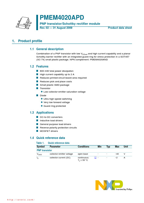
PMEM4020APD,115;中文规格书,Datasheet资料
1.Product profile1.1General descriptionCombination of a PNP transistor with low V CEsat and high current capability and a planar Schottky barrier rectifier with an integrated guard ring for stress protection in a SOT457(SC-74) small plastic package. NPN complement: PMEM4020AND1.2FeaturesI 600 mW total power dissipation I High current capability up to 2 AI Reduces printed-circuit board area required I Reduces pick and place costs I Small plastic SMD package ITransistorN Low collector-emitter saturation voltage I DiodeN Ultra high-speed switching N Very low forward voltage N Guard ring protected1.3ApplicationsI DC-to-DC converters I Inductive load driversI General purpose load driversI Reverse polarity protection circuits IMOSFET drivers1.4Quick reference dataPMEM4020APDPNP transistor/Schottky rectifier moduleRev. 02 — 31 August 2009Product data sheetTable 1.Quick reference data Symbol ParameterConditions Min Typ Max Unit PNP transistorV CEO collector-emitter voltage open base --−40V I Ccollector current (DC)continuous;T s ≤ 55°C[1]--−2A[1]Soldering point of collector or cathode tab.2.Pinning information3.Ordering information4.Marking5.Limiting valuesSchottky barrier rectifierV R continuous reverse voltage --40V I Fcontinuous forward current--1ATable 1.Quick reference data …continued Symbol ParameterConditionsMin Typ Max Unit Table 2.Discrete pinningPin Description Simplified outline Symbol1emitter 2not connected 3cathode 4anode 5base 6collector132456sym04036145Table 3.Ordering informationType numberPackage NameDescriptionVersion PMEM4020APDSC-74plastic surface mounted package; 6 leadsSOT457Table 4.MarkingType number Marking code PMEM4020APDD3Table 5.Limiting valuesIn accordance with the Absolute Maximum Rating System (IEC 60134).Symbol ParameterConditions Min Max Unit PNP transistorV CBO collector-base voltage open emitter -−40V V CEO collector-emitter voltage open base -−40V V EBOemitter-base voltageopen collector-−5V[1]Mounted on a FR4 printed-circuit board, single-sided copper, tin-plated, standard footprint.[2]Device mounted on a printed-circuit board, single-sided copper, tin-plated, 1cm 2 mounting pad for both collector and cathode.[3]Mounted on a ceramic printed-circuit board, single-sided copper, tin-plated, standard footprint.[4]Soldering point of collector or cathode tab.I Ccollector current (DC)continuous [1]-−0.75A continuous [2]-−1A continuous [3]-−1.3A continuous;T s ≤ 55°C[4]-−2A I CM peak collector current -−3A I BM peak base current -−1A P tottotal power dissipationT amb ≤ 25°C [1]-295mW T amb ≤ 25°C [2]-400mW T amb ≤ 25°C [3]-500mW T s ≤ 55°C[4]-1000mW T j junction temperature -150°C Schottky barrier rectifierV R continuous reverse voltage -40V I F continuous forward voltage -1A I FRM repetitive peak forward currentt p ≤ 1 ms;δ≤ 0.5- 3.5A I FSM non-repetitive peak forward currentt = 8 ms; square wave -10A P tottotal power dissipationT amb ≤ 25°C [1]-295mW T amb ≤ 25°C [2]-400mW T amb ≤ 25°C [3]-500mW T s ≤ 55°C[4]-1000mW T j junction temperature [2]-150°C Combined deviceP tot total power dissipation T amb ≤ 25°C[2]-600mW T stg storage temperature −65+150°C T ambambient temperature[2]−65+150°CTable 5.Limiting values …continuedIn accordance with the Absolute Maximum Rating System (IEC 60134).Symbol ParameterConditions Min Max Unit6.Thermal characteristics[1]For Schottky barrier rectifiers thermal run-away has to be considered, as in some applications the reverse power losses P R are a significant part of the total power losses. Nomograms for determining the reverse power losses P R and I F(AV) rating will be available on request.[2]Soldering point of collector or cathode tab.[3]Mounted on a ceramic printed-circuit board, single-sided copper, tin-plated, standard footprint.[4]Device mounted on a printed-circuit board, single-sided copper, tin-plated, 1cm 2 mounting pad for both collector and cathode tab.[5]Mounted on a FR4 printed-circuit board, single-sided copper, tin-plated, standard footprint.Table 6.Thermal characteristics [1]Symbol Parameter Conditions Min Typ Max Unit Single device R th(j-s)thermal resistance from junction to soldering point in free air [2]--95K/W R th(j-a)thermal resistance from junction to ambientin free air[3]--250K/W [4]--315K/W [5]--425K/W Combined device R th(j-a)thermal resistance from junction to ambientin free air[3]--208K/W7.Characteristics[1]Pulse test: t p ≤ 300µs;δ≤ 0.02Table 7.CharacteristicsT amb = 25°C unless otherwise specified Symbol ParameterConditionsMin Typ Max Unit PNP transistorI CBOcollector-base cut-off current V CB =−40 V; I E = 0 A --−100nA V CB =−40 V; I E = 0 A;T j = 150°C--−50µA I CEO collector-emitter cut-off current V CE =−30 V; I B = 0 A --−100nA I EBO emitter-base cut-off current V EB =−5 V; I C = 0 A --−100nAh FEDC current gainV CE =−5 V; I C =−1 mA 300--V CE =−5 V; I C =−100 mA 300--V CE =−5 V; I C =−500 mA 250-900V CE =−5 V; I C =−1 A 160--V CE =−5 V; I C =−2 A[1]50--V CEsatcollector-emitter saturation voltageI C =−100 mA; I B =−1 mA --−120mV I C =−500 mA; I B =−50 mA --−145mV I C =−1 A; I B =−100 mA --−260mV I C =−2 A; I B =−200 mA--−530mV R CEsat equivalent on-resistance I C =−1 A; I B =−100 mA [1]-180280m ΩV BEsat base-emittersaturation voltage I C =−1 A; I B =−100 mA [1]--−1.1V V BEon base-emitter turn-on voltageV CE =−5 V; I C =−1 A [1]--−1.0V f T transition frequency V CE =−10 V; I C =−50 mA;f = 100 MHz150--MHz C ccollector capacitanceV CB =−10 V; I E = i e = 0 A;f = 1 MHz --10pFSchottky barrier rectifier V Fcontinuous forward voltagesee Figure 1I F = 0.1 mA [1]-95130mV I F = 1 mA [1]-155210mV I F = 10 mA [1]-220270mV I F = 100 mA [1]-295350mV I F = 1000 mA[1]-540640mV I Rreverse currentsee Figure 2V R = 10 V [1]-720µA V R = 40 V[1]-30100µA C ddiode capacitanceV R = 1 V; f = 1 MHz;see Figure 3-4348pFSchottky barrier rectifier (1)T amb =150°C (2)T amb =85°C (3)T amb =25°CSchottky barrier rectifier (1)T amb =150°C (2)T amb =85°C (3)T amb =25°CFig 1.Forward current as a function of forward voltage; typical valuesFig 2.Reverse current as a function of reverse voltage; typical valuesSchottky barrier rectifier;T amb = 25°C; f = 1 MHzPNP transistor;V CE =−5 V (1)T amb = 150°C (2)T amb = 25°C (3)T amb =−55°CFig 3.Diode capacitance as a function of reverse voltage; typical valuesFig 4.DC current gain as a function of collector current; typical values0.60.40.2010310210110−1mdb669I F (mA)V F (V)(1)(2)(3)020103040V R (V)mdb670105104103102101I R (µA)(1)(2)(3)05102010008015604020mdb671V R (V)C d (pF)012002004006008001000mhc088−10−1h FE −10−1I C (mA)−102−103−104(1)(2)(3)PNP transistor;V CE =−5 V (1)T amb =−55°C (2)T amb = 25°C (3)T amb = 150°CPNP transistor;I C /I B = 10(1)T amb = 150°C (2)T amb = 25°C (3)T amb =−55°CFig 5.Base-emitter voltage as a function of collector current; typical valuesFig 6.Collector-emitter saturation voltage as a function of collector current; typical valuesPNP transistor;I C /I B = 10(1)T amb = 150°C (2)T amb = 25°C (3)T amb =−55°CPNP transistor;V CE =−10 VFig 7.Equivalent on-resistance as a function of collector current; typical valuesFig 8.Transition frequency as a function of collector current−10−1−10−1mhc089−10−1−1−10V BE (V)I C (mA)−103−102−104(1)(2)(3)−103−102−10−1mhc090−1−10V CEsat (mV)I C (mA)−102−103−104(1)(2)(3)10110−1102mhc091−10−1−1−10R CEsat (Ω)I C (mA)−103−102−104(1)(2)(3)0−100030010020025050150−200−400f T (MHz)I C (mA)−600−800mhc0928.Application informationFig 9.DC-to-DC converterFig 10.Inductive load driver (relays, motors andbuzzers) with free-wheeling diodemgu866V OUTV INCONTROLLERmgu867V CCIN9.Package outlineFig 11.Package outline SOT457 (SC-74)REFERENCESOUTLINE VERSION EUROPEAN PROJECTIONISSUE DATE IECJEDECJEITA SOT457SC-74w BM b pD epin 1indexAA 1L pQdetail XH EE v M AA B yscalecX13245601 2 mmPlastic surface-mounted package (TSOP6); 6 leadsSOT457UNIT A 1b p c D E H E L p Q y w v mm0.10.0130.400.253.12.70.260.101.71.3e 0.953.02.50.20.10.2DIMENSIONS (mm are the original dimensions)0.60.20.330.23A 1.10.905-11-0706-03-1610.Packing informationTable 8.Packing methodsThe indicated -xxx are the last three digits of the 12NC ordering code.[1]Type number Package Description Packing quantity300010000 PMEM4020APD SOT457 4 mm pitch, 8 mm tape and reel; T1-115-1354 mm pitch, 8 mm tape and reel; T2-125-165 [1]For further information and the availability of packing methods, see Section13.分销商库存信息: NXPPMEM4020APD,115。
Tektronix DMM4020数字多功能表数据手册说明书

Digital MultimetersTektronix DMM4020DataSheetDMM4020Features &Bene fitsKey Performance Speci fications 5.5Digit ResolutionBasic VDC Accuracy of up to 0.015%(1yr.)200mV to 1000V Voltage Range,with up to 10μV Resolution 200μA to 10A Current Range,with up to 1nA Resolution 200Ωto 100M ΩOhm Range,with up to 1m ΩResolution CAT I 1000V,CAT II 600VAvailable Functions and Features Volts,Ohms,and Amps Measurements Diode and Continuity Testing Frequency Measurements2×4Ohms 4-wire Measurement Technique Dedicated DC Leakage Current MeasurementsSix Dedicated Buttons for Fast Access to Instrument Setups Limit Compare Mode for Pass/Fail TestingConnectivityFront 2×4Measurement InputsRS-232on Rear Panel for Quick PC Connectivity Includes USB to RS-232Interface Adapter CableIncludes National Instrument’s LabVIEW SignalExpress™TE Limited Edition for Connecting Your Bench3-yearWarrantyData SheetMeasurements with the Push of a ButtonAs the circuits in embedded system designs become more sophisticated, you must measure a multitude of different parameters to validate your design.The Tektronix DMM40205.5digit bench multimeter offers a broad range of functions in one easy-to-use instrument.Typical multimeter measurements–volts,ohms,and amps–are made with a basic VDC accuracy of up to0.015%,ensuring you have the performance you need for your design.You can also use the DMM4020to measure frequency,and to perform continuity and diode tests.This allows youto replace your counter,continuity tester,and DMM with one versatile instrument,saving bench space and cost.Measure Nanoampere SignalsMeasuring standby current in today’s energy-efficient designs requires looking at very low currents,often in the microamp or nanoamp range. Using a traditional multimeter for this measurement can lead to inaccurate results since they typically employ the shunt resistance technique for measuring current.The DMM4020offers an improved method for measuring low currents.By using a current-to-voltage op amp technique,the DMM4020can make current measurements with1nA of resolution and with minimal loading affect on the circuit under test,giving results that reflect real-world operation of the device.Designed to Make Your Work EasierThe DMM4020multimeter is designed with the ease-of-use and familiar operation you expect from Tektronix.Intuitive OperationDedicated front-panel buttons provide fast access to frequently used functions and parameters,reducing setup time.You no longer need to search through software menus tofind the function youneed.Limit compare mode on the DMM4020.Setup Buttons for Your Common MeasurementsWith six setup buttons on the front panel,you can save the settings for your most common measurements.Simply set up the meter for a measurement, then press shift followed by a setup button to save the measurement settings.Now each time you perform that measurement,you simply press the appropriate setup key.Dual DisplayWith the unique dual display,you can measure two different parameters of the same signal from one test connection.Limit CompareThe limit compare mode provides pass/fail indicators to quickly show if a test passes or fails to help eliminate mistakes,especially for results that are close to the limit.Simple and Accurate4-wire MeasurementsPatented split terminal jacks for the2×4ohms function allow you to perform 4-wire measurements using only two leads instead of four.Special test lead accessories are available to enable you to establish the connection.You get excellent resolution and accuracy plus the convenience and ease of using a single pair of leads.Easy Connectivity to Your PCThe RS-232port on the back panel can be used to connect to your PC.A USB to RS-232interface adapter cable is included standard with the DMM4020for connecting to your PC’s USB port.Digital Multimeters—TektronixDMM4020Signal Express acquiring data from Tektronix DMM4020and DPO3052.Connect Your Bench for Intelligent Debug Easily capture,save,and analyze measurement results from your multimeter with the special Tektronix Edition of National Instrument’s LabVIEW SignalExpress™software.Every DMM4020multimeter ships with a free copy of the Limited Edition version of SignalExpress for basic instrument control,data logging,and analysis.The optional Professional Edition offers over200built-in functions that provide additional signal processing,advanced analysis,sweeping,limit testing,and user-defined step capabilities.SignalExpress supports the range of Tektronix bench instruments*1, enabling you to connect your entire test bench.You can then accessthe Signal Express used to export DMM4020data into Excel.feature-rich tools packed into each instrument from one intuitive software interface.This allows you to automate complex measurements requiring multiple instruments,log data for an extended period of time,time-correlate data from multiple instruments,and easily capture and analyze your results, all from your PC.Only Tektronix offers a connected test bench of intelligent instruments to simplify and speed debug of your complex design. Performance You Can Count OnIn addition to industry-leading service and support,every DMM4020 multimeter comes backed with a three-year standard warranty.*1NI LabVIEW Signal Express supports the following Tektronix instruments:MSO/DPO4000/3000/2000 Series oscilloscopes,TDS3000C/2000B/1000B Series oscilloscopes,AFG3000Series arbitrary/function generators,DMM4050/4040/4020Series digital multimeters.3Data SheetCharacteristics General SpecificationsVoltageCharacteristic Description100V Setting90V to110V120V Setting108V to132V220V Setting198V to242V240V Setting216V to264VFrequency47Hz to440HzPower Consumption15VA peak(10W average)DimensionsDimension mm in. Height88 3.46Width2178.56 Depth29711.7 Weight kg lb.Net 2.1 4.6DisplayVacuum Fluorescent Display,segmentEnvironmentCharacteristic DescriptionTemperatureOperating0°C to50°CStorage-40°C to70°CWarm Up½hour to full uncertainty specificationsRelative Humidity(noncondensing)Operating Uncontrolled(<10°C)<90%(10°C to28°C)<75%(28°C to40°C)<45%(40°C to50°C)Storage<95%(-40°C to70°C)AltitudeOperating2,000metersStorage12,000metersVibration Complies with MIL-PRF-28800F Class3Safety Complies with IEC61010-1:2001,ANSI/ISA61010-1(S82.02.01):2004,UL61010-1:2004,CAN/CSA C22.2No.61010.1:2004,CAT I1000V/CAT II600VEMC Designed to comply with IEC61326-1:1997+A1:1998+A2:2000TriggeringCharacteristic DescriptionTrigger Delay400msExternal Trigger Delay<2msExternal Trigger Jitter<1msTrigger Input TTL LevelsTrigger Output5V maxMath FunctionsMin/max,relative,hold,compare,and dB functionsElectricalCharacteristic DescriptionInput Protection1000V all rangesOverrange10%on the largest ranges of all functions exceptcontinuity and diode testRemote InterfacesRS-232C(RS-232to USB Adapter cable included)WarrantyThree yearsDigital Multimeters—Tektronix DMM4020Electrical SpecificationsDC Voltage SpecificationsSpecifications are valid for5½digit mode and after at least a half-hour warm-up.Characteristic DescriptionMaximum Input1000V on any rangeCommon ModeRejection120dB at50or60Hz0.1%(1kΩunbalance)Normal Mode Rejection80dB at Slow RateA/D Nonlinearity15ppm of rangeInput Bias Current<30pA at25°CSettling Considerations Measurement settling times are affected by sourceimpedance,cable dielectric characteristics,and inputsignal changesInput CharacteristicsResolutionRange Full Scale(5½Digits)Slow Medium FastInput Impedance 200mV199.999mV1V10μV10μV>10GΩ*22V 1.99999V10μV100μV100μV>10GΩ*220V19.9999V100μV1000μV1000μV10MΩ±1%200V199.999V1mV10mV10mV10MΩ±1%1000V1000.00V10mV100mV100mV10MΩ±1%*2At some dual-display measurements,the input impedance of200mV and2V ranges may be changed to10MΩ.AccuracyUncertainty*390days1year Range23°C±5°C23°C±5°C Temperature Coefficient/°C Outside18–28°C200mV0.01+0.0030.015+0.0040.0015+0.00052V0.01+0.0020.015+0.0030.001+0.000520V0.01+0.0030.015+0.0040.0020+0.0005200V0.01+0.0020.015+0.0030.0015+0.00051000V0.01+0.0020.015+0.0030.0015+0.0005*3Uncertainty given as±(%of reading+%of range).5Data SheetAC Voltage SpecificationsAC Voltage specifications are for AC sinewave signals>5%of range.For inputs from 1%to5%of range and<50kHz,add an additional error of0.1%of range,and for 50kHz to100kHz,add0.13%of range.Characteristic DescriptionMaximum Input750V RMS or1000V peak or8×107Volts-Hertz product Measurement Method AC-coupled true RMS.Measures the AC component ofinput with up to1000VDC bias on any rangeAC Filter Bandwidth20Hz–100kHzCommon ModeRejection60dB at50Hz or60Hz(1kΩunbalance)Maximum Crest Factor3:1at Full ScaleAdditional Crest Factor Errors(<100Hz)Crest Factor1-2,0.05%of full scale Crest Factor2-3,0.2%of full scale Only applies for non-sinusoid signalsInput CharacteristicsResolutionRange Full Scale(5½Digits)Slow Medium FastInput Impedance200mV199.999mV1μV10μV10μV 2V 1.99999V10μV100μV100μV 20V19.9999V100μV1000μV1000μV 200V199.999V1mV10mV10mV 750V750.00V10mV100mV100mV 1MΩ±2%shunted by<100pfAccuracyUncertainty*390days1year Range Frequency23°C±5°C23°C±5°C Temperature Coefficient/°C Outside18–28°C20Hz–45Hz0.8+0.050.9+0.050.01+0.00545Hz–20kHz0.15+0.050.2+0.050.01+0.00520kHz–50kHz0.3+0.050.35+0.050.01+0.005 200mV50kHz–100kHz0.8+0.050.9+0.050.05+0.0120Hz–45Hz0.8+0.050.9+0.050.01+0.00545Hz–20kHz0.15+0.050.2+0.050.01+0.00520kHz–50kHz0.3+0.050.35+0.050.01+0.005 2V50kHz–100kHz0.8+0.050.9+0.050.05+0.0120Hz–45Hz0.8+0.050.9+0.050.01+0.00545Hz–20kHz0.15+0.050.2+0.050.01+0.00520kHz–50kHz0.3+0.050.35+0.050.01+0.005 20V50kHz–100kHz0.8+0.050.9+0.050.05+0.0120Hz–45Hz0.8+0.050.9+0.050.01+0.00545Hz–20kHz0.15+0.050.2+0.050.01+0.00520kHz–50kHz0.3+0.050.35+0.050.01+0.005 200V50kHz–100kHz0.8+0.050.9+0.050.05+0.0120Hz–45Hz0.8+0.050.9+0.050.01+0.00545Hz–20kHz0.15+0.050.2+0.050.01+0.00520kHz–50kHz0.3+0.050.35+0.050.01+0.005 750V50kHz–100kHz0.8+0.050.9+0.050.05+0.01 *3Uncertainty given as±(%of reading+%of range).Digital Multimeters—Tektronix DMM4020 ResistanceSpecifications are for4-wire resistance function,or2-wire resistance with REL.IfREL is not used,add0.2Ωfor2-wire resistance plus lead resistance.Characteristic DescriptionMeasurement Method Current source referenced to LO inputMax Lead Resistance (4-wire ohms)10%of range per lead for200Ω,2kΩranges.1kΩper lead on all other ranges.Input Protection1000V on all rangesInput CharacteristicsResolutionRange Full Scale(5½Digits)Slow Medium FastCurrent Source200Ω199.999Ω0.001Ω0.01Ω0.01Ω0.8mA2kΩ 1.99999kΩ0.01Ω0.1Ω0.1Ω0.8mA20kΩ19.9999kΩ0.1Ω1Ω1Ω0.08mA 200kΩ199.999kΩ1Ω10Ω10Ω0.008mA2MΩ 1.99999MΩ10Ω100Ω100Ω0.9μA20MΩ19.9999MΩ100Ω1kΩ1kΩ0.16μA 100MΩ100.000MΩ1kΩ10kΩ10kΩ0.16μA||10MΩAccuracyUncertainty*390days1year Range23°C±5°C23°C±5°C Temperature Coefficient/°C Outside18–28°C200Ω0.02+0.0040.03+0.0040.003+0.00062kΩ0.015+0.0020.02+0.0030.003+0.000520kΩ0.015+0.0020.02+0.0030.003+0.0005200kΩ0.015+0.0020.02+0.0030.003+0.00052MΩ0.03+0.0030.04+0.0040.004+0.000520MΩ0.2+0.0030.25+0.0030.01+0.0005100MΩ 1.5+0.004 1.75+0.0040.2+0.0005*3Uncertainty given as±(%of reading+%of range).7Data SheetDC CurrentCharacteristic DescriptionInput Protection Tool-accessible11A/1000V and440mA/1000VfusesShunt Resistance0.01Ωfor2A and10A ranges1Ωfor20mA and200mABurden voltage<5mV for200μA and2mA rangeInput CharacteristicsResolutionRange Full Scale(5½Digits)Slow Medium FastBurden Voltage 200μA199.999μA0.001μA0.01μA0.01μA<5mV2mA1999.99μA0.01μA0.1μA0.1μA<5mV20mA19.9999mA0.1μA1μA1μA<0.05V 200mA19.9999mA1μA10μA10μA<0.5V2A 1.99999A10μA100μA100μA<0.1V10A10.0000A100μA1mA1mA<0.5V AccuracyUncertainty*390days1year Range23°C±5°C23°C±5°C Temperature Coefficient/°C Outside18–28°C200μA0.02+0.0050.03+0.0050.003+0.001 2mA0.015+0.0050.02+0.0050.002+0.001 20mA0.03+0.020.04+0.020.005+0.001 200mA0.02+0.0050.03+0.0080.005+0.001 2A0.05+0.020.08+0.020.008+0.001 10A0.18+0.010.2+0.010.008+0.001 *3Uncertainty given as±(%of reading+%of range).Digital Multimeters—Tektronix DMM4020 AC CurrentThe following AC current specifications are for sinusoidal signals with amplitudesgreater than5%of range.For inputs from1%to5%of range,add an additionalerror of0.1%of range.Characteristic DescriptionInput Protection Tool-accessible11A/1000V and440mA/1000VfusesMeasurement Method AC-coupled true RMSShunt Resistance0.01Ωfor2A and10A ranges1Ωfor20mA and200mAAC Filter Bandwidth20Hz–100kHzMaximum Crest Factor3:1at Full ScaleAdditional Crest Factor Errors(<100Hz)Crest Factor1-2,0.05%of full scale Crest Factor2-3,0.2%of full scale Only applies to non-sinusoid signalsInput CharacteristicsResolutionRange Full Scale(5½Digits)Slow Medium FastBurden Voltage 20mA19.9999mA0.1μA1μA1μA<0.05V 200mA199.999mA1μA10μA10μA<0.5V2A 1.99999A10μA100μA100μA<0.1V10A10.0000A100μA1mA1mA<0.5V AccuracyUncertainty*390days1year Range Frequency23°C±5°C23°C±5°C Temperature Coefficient/°C Outside18–28°C20Hz-45Hz1+0.05 1.25+0.060.015+0.00520mA45Hz-2kHz0.25+0.050.3+0.060.015+0.00520Hz-45Hz0.8+0.051+0.060.015+0.005200mA45Hz-2kHz0.25+0.050.3+0.060.015+0.00520Hz-45Hz1+0.05 1.25+0.060.015+0.0052A45Hz-2kHz0.25+0.050.3+0.060.015+0.00520Hz-45Hz1+0.1 1.25+0.120.015+0.00510A45Hz-2kHz1+0.10.5+0.120.015+0.005*3Uncertainty given as±(%of reading+%of range).9Data SheetFrequencyCharacteristic Description Gate Time131msMeasurement Method AC-coupled input using the AC voltage measurement functionSettling Considerations When measuring frequency after a DC offset voltage change,errors may occur.For the most accurate measurement,wait up to1second to allow input-blocking RC time constant to settleMeasurement Considerations To minimize measurement errors,shield inputs from external noise when measuring low-voltage, low-frequency signalsInput CharacteristicsUncertainty90days1year Range Frequency23°C±5°C23°C±5°C Temperature Coefficient/°C Outside18–28°C20Hz–2kHz0.01+0.0020.01+0.0030.002+0.0012kHz–20kHz0.01+0.0020.01+0.0030.002+0.00120kHz–200kHz0.01+0.0020.01+0.0030.002+0.001 100mV to750V*4,5200kHz–1MHz0.01+0.0040.01+0.0060.002+0.002 *4Input>100mV.*5Limited to8×107V Hz.ContinuityCharacteristic Description Continuity Threshold20ΩTest Current1mAResponse Time100S/s with audible tone Rate FastMaximum Reading199.99ΩResolution0.01ΩDiode TestCharacteristic Description Response Time100S/s with audible tone Rate FastMaximum Reading 1.9999VResolution0.1mVDigital Multimeters—Tektronix DMM4020Ordering InformationModelsModel DescriptionDMM4020 5.5Digit MultimeterDMM4020Includes:Meter,TL710test leads,line cord,spare line fuse,statement of cal practices,Warranty statement,Safety and Installation Guide,Connectivity Installation Manual,CD-ROM with user manual(English,French,Italian,German, Spanish,Simplified Chinese,Traditional Chinese,Korean,Russian,Japanese), RS-232to USB Adapter Cable,National Instruments LabVIEW SignalExpress™Tektronix Edition,Limited Edition Software.Please specify power plug when ordering.Instrument OptionsPower Plug OptionsOption DescriptionOpt.A0North AmericaOpt.A1Universal EuroOpt.A2United KingdomOpt.A3AustraliaOpt.A5SwitzerlandOpt.A6JapanOpt.A10ChinaOpt.A11IndiaOpt.A99No power cordOpt.E1Euro and UK power cords Service Options*6Option DescriptionOpt.CA1Provides a single calibration event or coverage for thedesignated calibration interval,whichever comesfirst Opt.C3Calibration Service3YearsOpt.C5Calibration Service5YearsOpt.D1Calibration Data ReportOpt.R5Repair Service5Years(including warranty)*6Test Leads and accessories are not covered by the DMM warranty and Service Offerings.Refer to the datasheet of each Test Lead and accessory model for its unique warranty and calibration terms.Recommended Accessories and SoftwareAccessory DescriptionCalibration Manual077-0365-xxTL710Premium Test Leads(196-3250-xx)TL7052×4Wire Ohm1000V Precision Test LeadTL7252×4Wire Ohm SMD Test TweezersAC4000Soft Transit CaseHCTEK4321Hard Carrying CaseY8846S Single Rackmount KitY8846D Dual Rackmount Kit013-0369-xx Calibration Fixture4-terminal shortSIGEXPTE NI LabVIEW SignalExpress Tektronix Edition Software–FullVersionProduct(s)are manufactured in ISO registeredfacilities.Product(s)complies with IEEE Standard488.1-1987and RS-232C.11Data Sheet Contact Tektronix:ASEAN/Australasia(65)63563900Austria+41526753777Balkans,Israel,South Africa and other ISE Countries+41526753777Belgium078160166Brazil+55(11)3759-7627Canada1(800)661-5625Central East Europe,Ukraine,and the Baltics+41526753777Central Europe&Greece+41526753777Denmark+4580881401Finland+41526753777France+33(0)169868181Germany+49(221)9477400Hong Kong(852)2585-6688India(91)80-42922600Italy+39(02)250861Japan81(3)6714-3010Luxembourg+44(0)1344392400Mexico,Central/South America&Caribbean52(55)54247900Middle East,Asia,and North Africa+41526753777The Netherlands09002021797Norway80016098People’s Republic of China86(10)62351230Poland+41526753777Portugal800812370Republic of Korea82(2)6917-5000Russia&CIS+7(495)7484900South Africa+27112068360Spain(+34)901988054Sweden020*******Switzerland+41526753777Taiwan886(2)2722-9622United Kingdom&Ireland+44(0)1344392400USA1(800)426-2200For other areas contact Tektronix,Inc at:1(503)627-7111Updated5August2009For Further Information.Tektronix maintains a comprehensive,constantly expandingcollection of application notes,technical briefs and other resources to help engineers workingon the cutting edge of technology.Please visit Copyright©Tektronix,Inc.All rights reserved.Tektronix products are covered by U.S.and foreign patents,issued and rmation in this publication supersedes that in all previously published material.Specification and price change privileges reserved.TEKTRONIX and TEK are registered trademarks ofTektronix,Inc.All other trade names referenced are the service marks,trademarks,or registered trademarksof their respective companies.08Sep20093MW-24431-0。