24LC22A
24lc256系列中文
1.8-5.5V 400 kHz (2) 2.5-5.5V 400 kHz 1.8-5.5V 400 kHz(2) 2.5-5.5V 400 kHz 4.5V-5.5V 400 kHz
8 字节
16 字节 16 字节
整个阵列
整个阵列 无
无
A0, A1, A2 A0, A1, A2
I I, E
I I C, I, E
装。
封装类型 (1)
PDIP/SOIC
TSSOP/MSOP(2)
A0 1 A1 2 A2 3 VSS 4
8 VCC
A0 1
7 WP(3) A1 2
6 SCL
A2 3
5 SDA VSS 4
8 VCC
A0 A1
7 WP(3) NC NC
6 SCL NC
5
SDA
A2 VSS
TSSOP
1
14
2
13
3
12
4
11
1.8-5.5V 2.5-5.5V 1.8-5.5V
400 kHz (2)
400 kHz 1 MHz(3)
64 字节
整个阵列
A0, A1, A2(4)
I
P, SN, SM, ST, MS, MF,
I, E ST14
I
256 千位器件
24AA256
1.8-5.5V 400 kHz (2)
24LC256 24FC256
2005 Microchip Technology Inc.
DS21930A_CN 第 3 页
24AAXX/24LCXX/24FCXX
2.0 电气特性
绝对最大额定值 (†)
VCC.............................................................................................................................................................................6.5V 相对于 Vss 的所有输入和输出 ............................................................................................................ -0.6V 到 VCC +1.0V 存储温度 ................................................................................................................................................. -65°C 到 +150°C 环境温度 (使用电源时)........................................................................................................................ -40°C 到 +125°C 所有引脚静电保护 ....................................................................................................................................................................≥ 4 kV
24LC32A-MT资料

•ISO 7816 compliant contact locations•Single supply with operation down to 2.5V -Maximum write current 3 mA at 6.0V -Maximum read current 150 µ A at 6.0V -Standby current 1 µ A max at 2.5V•T wo wire serial interface bus, I 2 C ™ compatible •100 kHz (2.5V) and 400 kHz (5V) compatibility •Self-timed ERASE and WRITE cycles •Power on/off data protection circuitry•1,000,000 ERASE/WRITE cycles guaranteed •32 byte page or byte write modes available •Schmitt trigger inputs for noise suppression•Output slope control to eliminate ground bounce • 2 ms typical write cycle time, byte or page •Electrostatic discharge protection > 4000V •Data retention > 200 years•8-pin PDIP and SOIC packages •T emperature ranges:DESCRIPTIONThe Microchip T echnology Inc. 24LC32A is a 4K x 8(32K bit) Serial Electrically Erasable PROM in an ISO micromodule for use in smart card applications. The device has a page-write capability of up to 32 bytes.-Commercial: 0˚C to +70˚C2元器件交易网24LC32A MODULE1.0ELECTRICAL CHARACTERISTICS1.1Maximum Ratings*V CC ........................................................................7.0V All inputs and outputs w.r.t. V SS ......-0.6V to VCC +1.0V Storage temperature ..........................-65˚C to +150˚C Ambient temp. with power applied......-65˚C to +125˚C Soldering temperature of leads (10 seconds)..+300˚C ESD protection on all pins .....................................≥ 4 kV*Notice: Stresses above those listed under “Maximum Ratings”may cause permanent damage to the device. This is a stress rat-ing only and functional operation of the device at those or anyother conditions above those indicated in the operational listings of this specification is not implied. Exposure to maximum rating conditions for extended periods may affect device reliability.TABLE 1-1:PIN FUNCTIONSName Function V SS Ground SDA Serial Data SCL Serial ClockV CC+2.5V to 6.0V Power SupplyTABLE 1-2:DC CHARACTERISTICSVcc = +2.5V to 6.0VCommercial (C):T amb = 0˚C to +70 ° CParameterSymbolMinTypMaxUnitsConditionsSCL and SDA pins:High level input voltage V IH .7 V CC —V Low level input voltage V IL —.3 Vcc V Hysteresis of Schmitt T rigger inputsV HYS .05 V CC—V Note 1Low level output voltage V OL —.40V I OL = 3.0 mA @ V CC = 4.5V I OL = 2.1 mA @ V CC = 2.5V Input leakage current I LI -1010 µ A V IN = .1V to V CC Output leakage current I LO -1010 µ A V OUT = .1V to V CC Pin capacitance (all inputs/outputs)C IN ,C OUT —10pF V CC = 5.0V (Note 1)T amb = 25˚C, f c = 1 MHz Operating current I CC Write —3mA V CC = 6.0VI CC Read —400 µ A V CC = 6.0V , SCL = 400Khz Standby currentI CCS —1 µ A5 µ A SCL = SDA = V CC = 5.0VI CCS1µ AVCC = 2.5V (Note 1)Note 1:This parameter is periodically sampled and not 100% tested.元器件交易网24LC32A MODULETABLE 1-3:AC CHARACTERISTICSParameterSymbolVcc = 2.5 - 6.0V STD. MODE Vcc = 4.5 - 6.0V FAST MODE UnitsRemarksMinMaxMinMaxClock frequency F CLK —100—400kHz Clock high time T HIGH 4000—600—ns Clock low timeT LOW 4700—1300—ns SDA and SCL rise time T R —1000—300ns Note 1SDA and SCL fall time T F —300—300ns Note 1START condition hold timeT HD : STA 4000—600—ns After this period the first clock pulse is generatedST ART condition setup timeT SU : STA 4700—600—ns Only relevant for repeated ST ART conditionData input hold time T HD : DAT 0—0—ns Data input setup time T SU : DAT 250—100—ns STOP condition setup timeT SU : STO 4000—600—ns Output valid from clock T AA —3500—900ns Note 2Bus free timeT BUF 4700—1300—ns Time the bus must be free before a new transmission can start Output fall time from V IH min to V IL maxT OF —25020 +0.1C B 250ns Note 1, CB ≤ 100 pF Input filter spike sup-pression (SDA and SCL pins)T SP—50—50nsNote 3Write cycle timeTWR —5—5ms Byte or Page modeNote 1: Not 100% tested. CB = total capacitance of one bus line in pF .2: As a transmitter, the device must provide an internal minimum delay time to bridge the undefined region (minimum 300 ns) of the falling edge of SCL to avoid unintended generation of ST ART or STOP conditions. 3: The combined T SP and VHYSspecifications are due to Schmitt trigger inputs which provide improved noise and spike suppression. This eliminates the need for a Ti specification for standard operation.元器件交易网24LC32A MODULE2.0PIN DESCRIPTIONS2.1SDA (Serial Data)This is a bidirectional pin used to transfer addresses and data into and data out of the device. It is an open drain terminal, therefore the SDA bus requires a pullup resistor to V CC (typical 10K Ω for 100 kHz, 1K Ω for 400kHz)For normal data transfer SDA is allowed to change only during SCL low. Changes during SCL high are reserved for indicating the ST ART and STOP condi-tions.2.2SCL (Serial Clock)This input is used to synchronize the data transfer from and to the device.3.0FUNCTIONAL DESCRIPTIONThe 24LC32A supports a bidirectional two-wire bus and data transmission protocol. A device that sends data onto the bus is defined as transmitter, and a device receiving data as receiver. The bus must be con-trolled by a master device which generates the serial clock (SCL), controls the bus access, and generates the ST ART and STOP conditions, while the 24LC32A works as slave. Both master and slave can operate as transmitter or receiver but the master device deter-mines which mode is activated.元器件交易网24LC32A MODULE4.0BUS CHARACTERISTICSThe following bus protocol has been defined:•Data transfer may be initiated only when the bus is not busy.•During data transfer, the data line must remain stable whenever the clock line is HIGH. Changes in the data line while the clock line is HIGH will be interpreted as a ST ART or STOP condition.Accordingly, the following bus conditions have been defined (See Figure 4-1).4.1Bus not Busy (A)Both data and clock lines remain HIGH.4.2Start Data Transfer (B)A HIGH to LOW transition of the SDA line while the clock (SCL) is HIGH determines a ST ART condition.All commands must be preceded by a START condi-tion.4.3Stop Data Transfer (C)A LOW to HIGH transition of the SDA line while the clock (SCL) is HIGH determines a STOP condition. All operations must be ended with a STOP condition.4.4Data Valid (D)The state of the data line represents valid data when,after a ST ART condition, the data line is stable for the duration of the HIGH period of the clock signal.The data on the line must be changed during the LOW period of the clock signal. There is one clock pulse per bit of data.Each data transfer is initiated with a ST ART condition and terminated with a STOP condition. The number of the data bytes transferred between the ST ART and STOP conditions is determined by the master device.4.5AcknowledgeEach receiving device, when addressed, is obliged to generate an acknowledge signal after the reception of each byte. The master device must generate an extra clock pulse which is associated with this acknowledge bit.A device that acknowledges must pull down the SDA line during the acknowledge clock pulse in such a way that the SDA line is stable LOW during the HIGH period of the acknowledge related clock pulse. Of course,setup and hold times must be taken into account. Dur-ing reads, a master must signal an end of data to the slave by NOT generating an acknowledge bit on the last byte that has been clocked out of the slave. In this case, the slave (24LC32A) will leave the data line HIGH to enable the master to generate the STOP condition.(See Figure 4-2)元器件交易网24LC32A MODULE5.0DEVICE ADDRESSINGA control byte is the first byte received following the start condition from the master device. (See Figure 5-1) The control byte consists of a four bit control code;for the 24LC32A this is set as 1010 binary for read and write operations. The next three bits are device select bits on standard devices, however, for micromodules,these must be zeros. The last bit of the control byte defines the operation to be performed. When set to a one a read operation is selected, and when set to a zero a write operation is selected. The next two bytesreceived define the address of the first data byte (see Figure 5-2). Because only A11...A0 are used, the upper four address bits must be zeros. The most signif-icant bit of the most significant byte of the address is transferred first.Following the start condition, the 24LC32A monitors the SDA bus checking the device type identifier being transmitted. Upon receiving a valid control byte, the slave device outputs an acknowledge signal on the SDA line. Depending on the state of the R/W bit, the 24LC32A will select a read or write operation元器件交易网24LC32A MODULE6.0WRITE OPERATIONS6.1Byte WriteFollowing the start condition from the master, the con-trol code (four bits), the device select (three bits), and the R/W bit which is a logic low are clocked onto the bus by the master transmitter. This indicates to the addressed slave receiver that a byte with a word address will follow after it has generated an acknowl-edge bit during the ninth clock cycle. Therefore the next byte transmitted by the master is the high-order byte of the word address and will be written into the address pointer of the 24LC32A MODULE. The next byte is the least significant address byte. After receiving another acknowledge signal from the 24LC32A the master device will transmit the data word to be written into the addressed memory location.The 24LC32A acknowledges again and the master generates a stop condition. This initiates the internal write cycle, and during this time the 24LC32A will not generate acknowledge signals (see Figure 6-1).6.2Page WriteThe write control byte, word address and the first data byte are transmitted to the 24LC32A in the same way as in a byte write. But instead of generating a stop con-dition, the master transmits up to 32 bytes which are temporarily stored in the on-chip page buffer and will be written into memory after the master has transmitted a stop condition. After receipt of each word, the five lower address pointer bits are internally incremented by one.If the master should transmit more than 32 bytes prior to generating the stop condition, the address counter will roll over and the previously received data will be overwritten. As with the byte write operation, once the stop condition is received, an internal write cycle will begin. (see Figure 6-2).元器件交易网24LC32A MODULE7.0ACKNOWLEDGE POLLINGSince the device will not acknowledge during a write cycle, this can be used to determine when the cycle is complete (this feature can be used to maximize bus throughput). Once the stop condition for a write com-mand has been issued from the master, the device ini-tiates the internally timed write cycle. ACK polling can be initiated immediately. This involves the master send-ing a start condition followed by the control byte for a write command (R/W = 0). If the device is still busy with the write cycle, then no ACK will be returned. If the cycle is complete, then the device will return the ACK and the master can then proceed with the next read or write command. See Figure 7-1 for flow diagram.FIGURE 7-1:ACKNOWLEDGE POLLING8.0READ OPERATIONRead operations are initiated in the same way as write operations with the exception that the R/W bit of the slave address is set to one. There are three basic types of read operations: current address read, random read,and sequential read.8.1Current Address ReadThe 24LC32A contains an address counter that main-tains the address of the last word accessed, internally incremented by one. Therefore, if the previous access (either a read or write operation) was to address n (n is any legal address), the next current address read oper-ation would access data from address n + 1. Upon receipt of the slave address with R/W bit set to one, the 24LC32A issues an acknowledge and transmits the eight bit data word. The master will not acknowledge the transfer but does generate a stop condition and the 24LC32A discontinues transmission (see Figure 8-1).8.2Random ReadRandom read operations allow the master to access any memory location in a random manner. T o perform this type of read operation, first the word address must be set. This is done by sending the word address to the 24LC32A as part of a write operation (R/W bit set to 0).After the word address is sent, the master generates a start condition following the acknowledge. This termi-nates the write operation, but not before the internal address pointer is set. Then the master issues the con-trol byte again but with the R/W bit set to a one. The 24LC32A will then issue an acknowledge and transmit the eight bit data word. The master will not acknowl-edge the transfer but does generate a stop condition which causes the 24LC32A to discontinue transmis-sion (see Figure 8-2).元器件交易网24LC32A MODULE8.3Sequential ReadSequential reads are initiated in the same way as a ran-dom read except that after the 24LC32A transmits the first data byte, the master issues an acknowledge as opposed to the stop condition used in a random read.This acknowledge directs the 24LC32A to transmit the next sequentially addressed 8 bit word (see Figure 8-3). Following the final byte transmitted to the master,the master will NOT generate an acknowledge but will generate a stop condition.To provide sequential reads the 24LC32A contains an internal address pointer which is incremented by one at the completion of each operation. This address pointer allows the entire memory contents to be serially read during one operation. The internal address pointer will automatically roll over from address 0FFF to address 000 if the master acknowledges the byte received from the array address 0FFF .元器件交易网24LC32A MODULE9.0SHIPPING METHODThe micromodules will be shipped to customers in clear plastic trays. Each tray holds 150 modules, and the trays can be stacked in a manner similar to shipping die in waffle packs. A tray drawing with dimensions is shown in Figure 9-1.元器件交易网24LC32A MODULE元器件交易网24LC32A MODULENOTES:元器件交易网24LC32A MODULENOTES:元器件交易网24LC32A MODULENOTES:元器件交易网24LC32A MODULE24LC32A MODULE PRODUCT IDENTIFICATION SYSTEMT o order or obtain information, e.g., on pricing or delivery, refer to the factory or the listed sales office.Sales and SupportData SheetsProducts supported by a preliminary Data Sheet may have an errata sheet describing minor operational differences and recom-mended workarounds. To determine if an errata sheet exists for a particular device, please contact one of the following:1.Y our local Microchip sales office.2.The Microchip Corporate Literature Center U.S. FAX: (602) 786-7277.3.The Microchip’s Bulletin Board, via your local CompuServe number (CompuServe membership NOT required).Please specify which device, revision of silicon and Data Sheet (include Literature #) you are using.元器件交易网MAll rights reserved. © 1997, Microchip T echnology Incorporated, USA. 9/97 Printed on recycled paper.元器件交易网。
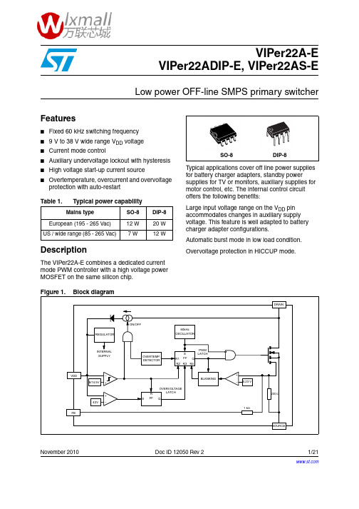
电源24VAC型号说明书

† UL File XAPX.E108966Fire & Smoke damper actuator ApplicationThe type FSLF spring-return actuator is intended for the operation of smoke and combination fire and smoke dampers in ventilation and air-conditioning systems. The actuator will meet requirements of UL555 and UL555S when tested as an assembly with the damper and will meet requirements of UBC for 15 second opening and closing. Square footage of damper operated will depend on make and model and the temperature required.IMPORTANT 24VDC NOTE: The FSLF24 & -S models will not operate below 24VDC. A filtered and regulated power supply must be used.OperationMounting of the actuator to the damper axle shaft or jackshaft is via a cold-weldclamp. Teeth in the clamp and V-bolt dig into the metal of both solid and hollow shafts maintaining a perfect connection. The specially designed clamp will not crush hollow shafts. The bottom end of the actuator is held by an anti-rotation strap or by a stud provided by the damper manufacturer.The actuator is mounted in its fail safe position with the damper blade(s) closed. Upon applying power, the actuator drives the damper to the open position. The internal spring is tensioned at the same time. If the power supply is interrupted, the spring moves the damper back to its fail-safe position.The FSLF draws higher peak current when driving against its end stop or any other type of stop. Given the technology of fuses & breakers, this requires the value of fuse or breaker to be increased to avoid nuisance opening or tripping. A 1 amp slow blow should be used for 24VAC. A 0.25 amp slow blow should be used for 120VAC. A .125 amp slow blow should be used for 230V. SAFETY NOTESWiring and installation must comply with all local electrical and mechanical codes.The actuator contains no components which the user can replace or repair. Cables are not plenum rated and require flex conduit.1/2” Threaded Connector: Screw a conduit fitting into the actuator’s metal bushing. Jacket the actuator’s input wiring with suitable fl exible conduit. Properly terminate the conduit in a suitable junction box.3/8” Flex Connector (-FC models): Mount the flexible conduit into theactuator’s metal bushing by means of the provided screw with a torque of 1.2 Nm. Jacket the actuator’s input wiring with suitable flexible conduit. Properly terminate the conduit in a suitable junction box.FSLF24 USOn/Off, Spring Return, 350°F [177°C] for a half hour, 15 Seconds Cycle TimeD a t e c r e a t e d , 03/08/2019 - S u b j e c t t o c h a n g e . © B e l i m o A i r c o n t r o l s (U S A ), I n c .Typical SpecificationAll smoke and combination fire and smoke dampers shall be providedwith Belimo FSTF, FSLF, FSNF, or FSAF actuators. All substitutions must be approved before submission of bid. Damper and actuator shall have UL 555S Listing for 250°F (350°F). Actuator shall have been tested to UL 2043 per requirements of IMC 602.2 and NEC 300.22 (c). Where position indication is required -S models with auxiliary switches or damper blade switches will be provided per code requirements.Wiring DiagramsAPPLICATION NOTESProvide overload protection and disconnect as required.45Actuators may be powered in parallel. Power consumption must beobserved.75Ground present on some models.FSLF24 USOn/Off, Spring Return, 350°F [177°C] for a half hour, 15 Seconds Cycle TimeDatecreated,3/8/219-Subjecttochange.©BelimoAircontrols(USA),Inc.。
VIPer22a电路图

之阿布丰王创作时间:二O二一年七月二十九日引言开关电源通过电路控制开关管进行高速的导通与截止, 将直流电转化为高频率的交流电提供给变压器进行变压, 从而发生所需要的一组或多组电压[ 1 ] 。
它具有效率高的特性, 而且开关电源的变压器体积比串联稳压型电源的要小得多, 电源电路比较整洁, 整机重量也有所下降, 所以成为当今电源发展的一种趋势。
本文采取V IPER22A芯片设计了一种开关电源。
2 V IPER22A芯片概述意法半导体的V IPER22A芯片为专用开关电源集成电路。
其内部结构如图1所示。
芯片工作时, 直流电压从漏极脚进入集成电路, 经整流和稳压后供给开关电源工作, 从而使这个电路工作时不需要外接启动电阻。
即使VDD供电电路不正常, 电源电路的振荡电路仍能起振, 而且图1 V IPER22A芯片内部结构电路有输出电压。
在VDD正常前, 由芯片内部自身供电, 经过很短时间后, VDD供电电源正常, 此时,利用门电路控制开关电路(ON /OFF)断开从栅极输入的供电回路。
V IPER22A 有过热、过压呵护功能。
VDD从4脚输入后, 首先送入比较器, 一旦输入VDD ≥42 V, 则触发器( FF1)输出一个置位信号1使控制振荡电路工作的触发器( FF2)输出为0,锁住U2 , 振荡信号无法输出, 即开关管不工作。
当输入电压小于1415 V时, U3 也将输出一个复位脉冲, 使开关管不工作。
当电路过热时, R1 为1,将FF2置0, 开关管不工作。
当供电电压VDD在正常范围时, FB所得的取样电压与基准电压0123 V相比较, 用其比较结果去控制FF2 的转换频率,从而控制开关管的状态转换, 实现控制输出电压,达稳压的功能。
该集成电路芯片内部包含60kHz的振荡电路, 其外围电路相当简单。
3 V IPER22A开关电源电路本文所使用的V IPER22A芯片具有优良的控制功能, 使得外围电路的设计较简单, 只需考虑一般的短路、过载电路呵护即可。
(任务一)彩色电视机电路综合分析方法介绍

( 任 务 一 彩 色 电 视 机 电 路 综 合 分 析 方 法 介 绍 ⑷、复合同步信号流程
为了进一步提高电视信号的稳定性,本机设有两 个同步分离电路。见以下方框图4-2所示。
)
图4-2 熊猫牌C54P38型彩色电视机 同步信号与行、场扫描信号流程图
( 任 务 一 彩 色 电 视 机 电 路 综 合 分 析 方 法 介 绍 行同步分离电路是由R610, C602,VD604等元件和 TA7698AP内部的同步分离电路共同组成。从N801的 40脚输出的全电视信号FBAS经 同步分离电路分离出 复合同步信号,一路在D7698AP内部直接送往行AFC 电路,去控制行振荡频率。场同步分离电路是由R606、 C607、R607、C608等元件构成。D7680AP的15脚输 出的全电视信号先经过L402和L407送音视频转换芯片 (12)脚,然后从(14)脚输出,经过C905耦合后到 进入D7698AP的(39)脚,在从(40)脚倒相输出 FBAS信号,经过R610、C602、VD604等元件组成的 行同步分离电路分离出复合同步信号送D7698AP的 (27)脚,然后从D7698AP的(26)脚输出复合同步 信号,再由R606, C607, R607, C608等组成的积分电 路从复合同步信号中分离出场同步信号。场同步信号 经C609耦合到TA7698AP的28脚,去控制场振荡频率。 )
2、围绕芯片,理顺信号 首先要根据整机电路图的结构形式,弄清是有哪块芯 片来完成相应电路的功能,然后根据芯片引脚功能来 判断信号的流程,具体可以根据以下思路理顺信号
)
( 任 务 一 彩 色 电 视 机 电 路 综 合 分 析 方 法 介 绍 ①高频电视图像信号从天线进入电视机,经过哪些电路和 哪些信号转换最终到达显像管。 ②高频伴音载频信号从天线进来后,经过哪些电路与哪些 信号转换到达扬声器。 ③同步信号从中频图像检波电路输出后,是经过哪些电路 和哪些信号转换到达行、场扫描的振荡电路。 ④行、场扫描信号是从振荡电路经过哪些电路到达行场偏 转线圈的。 ⑤高频电视载波信号从天线进入后经过高频头、中放电路 到检波电路以后才分离出图像信号、伴音信号、复合同步 信号等,分别送到解码电路、伴音电路和同步分离等对应 电路去。 通过以上过程,可以了解电视机中各信号在传输过程中进 行了哪些变化或变换,了解信号经过的各个电路的作用与 工作原理。这也是彩色电视机维修时判别故障部位的主要 依据。 )
SS24二极管参数

SS24二极管参数二极管(Diode)是最简单、最基本的电子元件之一,具有正向导通和反向截止的特性。
在市场上,有许多种不同类型的二极管,其中SS24是一种常见的快恢复二极管。
在以下文章中,将详细介绍SS24二极管的参数、结构、特性以及应用。
SS24二极管是一种快恢复二极管,也被称为超快恢复二极管(Ultrafast Rectifier Diode)。
它由PN结构组成,具有两个端子:阳极(Anode)和阴极(Cathode)。
SS24的封装常见的是DO-214AC(也被称为SMA)封装,方便焊接和安装。
1. 最大反向工作电压(Max Reverse Voltage):200V2. 平均整流电流(Average Rectified Current):2A3. 最大正向压降(Max Forward Voltage Drop):0.95V4. 最大反向漏电流(Max Reverse Leakage Current):5uA5. 正向导通时的导通电阻(Forward Voltage Drop):0.95V6. 正向持续电流(Continuous Forward Current):2A7. 快恢复时间(Reverse Recovery Time):50ns8. 工作温度范围(Operating Temperature Range):-65°C to +150°C1. 快恢复特性:SS24二极管具有快速的恢复时间(Reverse Recovery Time),可以在短时间内完成反向导通到截止的转变,减小了开关过程中的能量损耗,提高了效率。
2.高反向击穿电压:SS24二极管的最大反向工作电压为200V,可以在较高的电压下工作,适用于各种不同的电路应用。
3. 低导通压降:正向导通时的导通电阻(Forward Voltage Drop)仅为0.95V,能够减小功率损耗,提高效率。
4.高温工作能力:SS24二极管能够在-65°C到+150°C的工作温度范围内正常工作,适用于各种环境条件。
国产VIPer22A参考资料

VFB=2V; ID=1mA VFB=2V; VDS=500V ID=0.2A
IFB=2.0mA IFB=0.5mA;ID=50mA VDS=100V; VDD=5V
VFB=0V ID=0mA
最小 730
13 7 -
范围 典型
12 14.5 8 6.5 32 0.4 1.0 -220 60 560 700 0.9 1.23 300 700 150 30
业务电话:400-033-6518
-2-
sale@
Linkage
深圳市钲铭科电子有限公司
极限参数
极限参数(TA= 25℃)
符号
说明
VDS(max)
芯片 DRAIN 脚最高耐压
VDS(ST)
芯片启动时,DRAIN 脚最高耐压
VDD
芯片电源电压
深圳市钲铭科电子有限公司
电路图说明
上图中 D1-D4、C2 组成全波整流,D6、R1、C3 组成 RCD 吸收回路,消除变压器 T2 漏感产生的尖峰电压,
避免击穿 LKVIPER 22A 内部的高压 MOS 管。
输出部分 U3、U2、R5、R6、R3、R4、C8 组成采样反馈电路,R5、R6 决定系统的输出电压,输出电压 VOUT
Linkage
深圳市钲铭科电子有限公司
LKVIPER 22A
特点
85Vac~265Vac 宽电压输入 待机功耗小于 120mW@220Vac 集成高压启动电路 集成高压功率开关 60KHz 固定开关频率 9V~30V 宽 VDD 工作电压范围 电流模式 PWM 控制方式 内置过温、过流、过压、欠压
R7
33K
RT1
5D-9
VIPER22A中文资料_数据手册_参数
4
Operations . . . . . . . . . . . . . . . . . . . . . . . . . . . . . . . . . . . . . . . . . . . . . . . . . 7
4.1 Rectangular U-I output characteristics . . . . . . . . . . . . . . . . . . . . . . . . . . . . 7
Contents
VIPer22A-E, VIPer22ADIP-E, VIPer22AS-E
1
Electrical data . . . . . . . . . . . . . . . . . . . . . . . . . . . . . . . . . . . . . . . . . . . . . . 3
OVERTEMP. DETECTOR
S R1 FF Q R2 R3 R4
PWM LATCH
OVERVOLTAGE
R
LATCH
S FF Q
BLANKING
+ _ 0.23 V
1 kΩ
230 Ω SOURCE
November 2010
Doc ID 12050 Rev 2
1/21
21
Contents
SO-8
DIP-8
Typical applications cover off line power supplies for battery charger adapters, standby power supplies for TV or monitors, auxiliary supplies for motor control, etc. The internal control circuit offers the following benefits:
- 1、下载文档前请自行甄别文档内容的完整性,平台不提供额外的编辑、内容补充、找答案等附加服务。
- 2、"仅部分预览"的文档,不可在线预览部分如存在完整性等问题,可反馈申请退款(可完整预览的文档不适用该条件!)。
- 3、如文档侵犯您的权益,请联系客服反馈,我们会尽快为您处理(人工客服工作时间:9:00-18:30)。
2SHUDWLQJ .XUUHQW ' ' ' ² ² ² ² WHVWHG P$ P$ $ $ N+] 6&/ 6&/ 9&& 9&&
9&& 9 6'$ 9&& 9 6'$ 9&/. 9 66
1RWH
7KLV SDUDPHWHU LV SHULRGL.DOO\ VDPSOHG DQG QRW
$EVROXWH 0D[LPXP 5DWLQJV
9&& 9 $OO LQSXWV DQG RXWSXWV ZUW 966 9 WR 9 && 9 6WRUDJH WHPSHUDWXUH °& WR °& $PELHQW WHPS ZLWK SRZHU DSSOLHG °& WR °& 6ROGHULQJ WHPSHUDWXUH RI OHDGV VH.RQGV °& (6' SURWH.WLRQ RQ DOO SLQV ......................................................................................................................................................≥ N9 1RWL.H 6WUHVVHV DERYH WKRVH OLVWHG XQGHU ³0D[LPXP UDWLQJV´ PD\ .DXVH SHUPDQHQW GDPDJH WR WKH GHYL.H 7KLV LV D VWUHVV UDWLQJ RQO\ DQG IXQ.WLRQDO RSHUDWLRQ RI WKH GHYL.H DW WKRVH RU DQ\ RWKHU .RQGLWLRQV DERYH WKRVH LQGL.DWHG LQ WKH RSHUDWLRQDO OLVWLQJV RI WKLV VSH.LIL.DWLRQ LV QRW LPSOLHG ([SRVXUH WR PD[LPXP UDWLQJ .RQGLWLRQV IRU H[WHQGHG SHUL RGV PD\ DIIH.W GHYL.H UHOLDELOLW\
,QSXW OHYHOV RQ 9&/. SLQ
&,1 &287 3LQ .DSD.LWDQ.H DOO LQSXWVRXWSXWV ,&& :5,7( 2SHUDWLQJ .XUUHQW ,&& 5($' ,&&6 2SHUDWLQJ .XUUHQW 6WDQGE\ .XUUHQW
9&& 9 1RWH 7$0% & )&/. 9&& 9&& 9 9 6&/
'6$SDJH
0L.UR.KLS 7H.KQRORJ\ ,Q.
/&$
3DUDP 1R
$& &KDUD.WHULVWL.V
9.. 9 WR 9 ,QGXVWULDO , 7$0% 3DUDPHWHU &OR.N IUHTXHQ.\ &OR.N KLJK WLPH &OR.N ORZ WLPH 6'$ DQG 6&/ ULVH WLPH 6'$ DQG 6&/ IDOO WLPH 67$57 .RQGLWLRQ KROG WLPH 67$57 .RQGLWLRQ VHWXS WLPH 'DWD LQSXW KROG WLPH 'DWD LQSXW VHWXS WLPH 6723 .RQGLWLRQ VHWXS WLPH 2XWSXW YDOLG IURP .OR.N 1RWH %XV IUHH WLPH 7LPH WKH EXV PXVW EH IUHH EHIRUH D QHZ WUDQVPLVVLRQ .DQ VWDUW 2XWSXW IDOO WLPH IURP 9,+ PLQLPXP WR 9,/ PD[LPXP ,QSXW ILOWHU VSLNH VXSSUHVVLRQ 6'$ DQG 6&/ SLQV :ULWH .\.OH WLPH E\WH RU SDJH 2XWSXW YDOLG IURP 9&/. 9&/. KLJK WLPH 9&/. ORZ WLPH 9&/. VHWXS WLPH 9&/. KROG WLPH 0RGH WUDQVLWLRQ WLPH 7UDQVPLW2QO\ SRZHU XS WLPH ,QSXW ILOWHU VSLNH VXSSUHVVLRQ 9&/. SLQ (QGXUDQ.H WHVWHG &% 0LQ ² ² ² ² ² ² ² ² ² &% ² ² ² ² ² ² ² ² ² ² 0 WRWDO .DSD.LWDQ.H RI RQH EXV OLQH LQ S) 0D[ ² ² ² ² ² ² ² ² ² ² ² ² ² ² ² ² ² ² ² ² ² ² ² ² ² ² ² & WR & 8QLWV N+] QV QV QV QV QV QV QV QV QV QV QV &RQGLWLRQV 9 ≤ 9&& ≤ 9 9 ≤ 9&& ≤ 9 9 ≤ 9&& ≤ 9 9 ≤ 9&& ≤ 9 9 ≤ 9&& ≤ 9 9 ≤ 9&& ≤ 9 9 ≤ 9&& ≤ 9 1RWH 9 ≤ 9&& ≤ 9 1RWH 1RWH 9 ≤ 9&& ≤ 9 9 ≤ 9&& ≤ 9 9 ≤ 9&& ≤ 9 9 ≤ 9&& ≤ 9 1RWH 9 ≤ 9&& ≤ 9 9 ≤ 9&& ≤ 9 9 ≤ 9&& ≤ 9 9 ≤ 9&& ≤ 9 9 ≤ 9&& ≤ 9 9 ≤ 9&& ≤ 9 9 ≤ 9&& ≤ 9 9 ≤ 9&& ≤ 9 9 ≤ 9&& ≤ 9 1RWH 9 ≤ 9&& ≤ 9 1RWH 1RWHV DQG 6\P )&/. 7+,*+ 7/2: 75 7) 7+'67$ 76867$ 7+''$7 768'$7 768672 7$$ 7%8)
3LQV ODEHOHG µ1&¶ KDV QR LQWHUQDO .RQQH.WLRQV
%OR.N 'LDJUDP
+9 *(1(5$725 ,2 &21752/ /2*,& 0(025< &21752/ /2*,&
'HV.ULSWLRQ
7KH 0L.UR.KLS 7H.KQRORJ\ ,Q. /&$ LV D [ ELW GXDOPRGH (OH.WUL.DOO\ (UDVDEOH 3520 7KLV GHYL.H LV GHVLJQHG IRU XVH LQ DSSOL.DWLRQV UHTXLULQJ VWRUDJH DQG VHULDO WUDQVPLVVLRQ RI .RQILJXUDWLRQ DQG .RQWURO LQIRUPDWLRQ 7ZR PRGHV RI RSHUDWLRQ KDYH EHHQ LPSOH PHQWHG 7UDQVPLW2QO\ 0RGH .ELW DQG %LGLUH.WLRQDO 0RGH .ELW 8SRQ SRZHUXS WKH GHYL.H ZLOO EH LQ WKH 7UDQVPLW2QO\ 0RGH VHQGLQJ D VHULDO ELW VWUHDP RI WKH PHPRU\ DUUD\ IURP K WR )K .OR.NHG E\ WKH 9&/. SLQ $ YDOLG KLJK WR ORZ WUDQVLWLRQ RQ WKH 6&/ SLQ ZLOO .DXVH WKH GHYL.H WR HQWHU WKH WUDQVLWLRQ PRGH DQG ORRN IRU D YDOLG .RQWURO E\WH RQ WKH , & EXV ,I LW GHWH.WV D YDOLG .RQWURO E\WH IURP WKH PDVWHU LW ZLOO VZLW.K LQWR %L 'LUH.WLRQDO 0RGH ZLWK E\WH VHOH.WDEOH UHDGZULWH .DSD ELOLW\ RI WKH HQWLUH . PHPRU\ DUUD\ XVLQJ 6&/ ,I QR .RQWURO E\WH LV UH.HLYHG WKH GHYL.H ZLOO UHYHUW WR WKH 7UDQVPLW2QO\ 0RGH DIWHU LW UH.HLYHV .RQVH.XWLYH 9&/. SXOVHV ZKLOH WKH 6&/ SLQ LV LGOH 7KH /&$ LV DYDLODEOH LQ VWDQGDUG SLQ ',3 DQG 62,p;KDUD.WHULVWL.V
9.. 9 WR 9 ,QGXVWULDO , 7$0% &KDUD.WHULVWL. 0LQ 0D[ & WR & 8QLWV 7HVW &RQGLWLRQV
'6 &KDUD.WHULVWL.V 3DUDP 1R ' ' ' ' ' ' ' ' ' ' 6\P