2SD2074中文资料
2SD974资料

2SD974Silicon NPN Epitaxial
Application• Power switching• TV horizontal deflection output
Outline
321
1. Emitter2. Collector3. Base
TO-92MOD2SD974
2Absolute Maximum Ratings (Ta = 25°C)ItemSymbolRatingsUnitCollector to base voltageVCBO120V
Collector to emitter voltageVCEO60VEmitter to base voltageVEBO5VCollector currentIC1ACollector peak currentiC(peak)1.5ASurge collector currentIC(surge)4ACollector power dissipationPC0.9WJunction temperatureTj150°CStorage temperatureTstg–55 to +150°C
Electrical Characteristics (Ta = 25°C)ItemSymbolMinTypMaxUnitTest conditionsCollector to base breakdownvoltageV(BR)CBO120——VIC = 10 µA, IE = 0
Collector to emitter breakdownvoltageV(BR)CEO60——VIC = 1 mA, RBE = ∞Emitter to base breakdownvoltageV(BR)EBO5——VIE = 10 µA, IC = 0Collector cutoff currentICBO——1.0µAVCB = 100 V, IE = 0DC current transfer ratiohFE150——VCE = 5 V, IC = 1 A*1Collector to emitter saturationvoltageVCE(sat)——0.3VIC = 1 A, IB = 0.05 A*1
2SD2679资料

TransistorsRev.A 1/22A / 30V Bipolar transistor2SD2679z Applications z Dimensions (Unit : mm) Low frequency amplification, driverz Features1) Collector current is high.2) Low collector-emitter saturation voltage. (V CE(sat) ≤ 350mV at I C = 1.5A, I B = 75mA)z Structure NPN epitaxial planar silicon transistorz Absolute maximum ratings (T a=25°C) Power dissipation ParameterCollector-base voltage Collector-emitter voltage Emitter-base voltage Collector current Junction temperature Storage temperatureP C Symbol V CBO V CEO V EBO I C tj tstgLimits 3030620.52150−55 to +150Unit V V V A I CP DC Pulse4W °C °C∗1∗2∗3∗1 Pw=1ms, single pulse.∗2 Each terminal mounted on a recommended land.∗3 Mounted on a 40×40×0.7mm ceramic board.z Electrical characteristics (T a=25°C)ParameterConditionsCollector-base breakdown voltage I C =10µA Collector-emitter breakdown voltage I C =1mA Emitter-base breakdown voltage I E =10µA Collector cut-off current V CB =30V Emitter cut-off currentV EB =6VCollector-emitter saturation voltage I C /I B =1.5A/75mA DC current gain V CE =2V, I C =200mA Transition frequency V CE =2V, I E = −200mA , f=100MHzCollector output capacitanceSymbol BV CBO BV CEO BV EBO I CBO I EBO V CE(sat)∗∗ Pulsedh FE f T CobMin.30306−−−270−−Typ.−−−−−180−28020Max.−−−100100370680−−Unit VnA mV −MHz pF V CB =10V , IE =0mA , f=1MHzTransistorsRev.A 2/2z Electrical characteristics curvesFig.1 Grounded emitter propagation characteristics BASE TO EMITTER CURRENT : V BE (V)C O L L E C T O R C U R R E N T : I C (A )Fig.2 DC current gain vs. collector current0.0010.010.1110COLLECTOR CURRENT : I C (A)D C C U R R E N T G A I N : h F EFig.3 Collector-emitter saturation voltage base-emitter saturation voltage vs. collector current0.0010.010.1110COLLECTOR CURRENT : I C (A)C O L L E C T O R S A T U R A T I O N V O L T A G E : V C E (s a t ) (V )0.0010.010.1110COLLECTOR CURRENT : I C (A) B A S E S A T U R A T I O N V O L T A G E : V B E (s a t ) (V )Fig.4 Base-emitter saturation voltage vs. collector current Fig.5 Gain bandwidth product vs. emitter current1001000EMITTER CURRENT : I E (A)T R A N S I T I O N FR E Q U E N C Y : f T (M H z )Fig.6 Collector output chapacitance vs. collector-base voltage Emitter input capacitance vs. emitter-base voltageC O L L E C T O R O U T P U T C A P A C I T A N C E : C o b (p F )E M I T T E R I N P U T C A P A C I T A N C E : C i b (p F )COLLECTOR TO BASE VOLTAGE : V CB (V)EMITTER TO BASE VOLTAGE : V EB (V)Appendix1-Rev2.0Thank you for your accessing to ROHM product informations.More detail product informations and catalogs are available, please contact your nearest sales office.ROHM Customer Support SystemTHE AMERICAS / EUROPE / ASIA / JAPANContact us : webmaster@rohm.co.jpAppendix。
2SD2030资料

2SD2030, 2SD2031Silicon NPN EpitaxialApplicationLow frequency high voltage amplifierOutline2SD2030, 2SD20312Absolute Maximum Ratings (Ta = 25°C)ItemSymbol 2SD20302SD2031Unit Collector to base voltage V CBO 160200V Collector to emitter voltage V CEO 160200V Emitter to base voltage V EBO 55V Collector currentI C 100100mA Collector power dissipation P C 400400mW Junction temperature Tj 150150°C Storage temperatureTstg–55 to +150–55 to +150°CElectrical Characteristics (Ta = 25°C)ItemSymbolMin Typ Max Unit Test conditions Collector to base breakdown voltage 2SD2030V (BR)CBO 160——VI C = 10 µA, I E = 02SD2031200Collector to emitter breakdown voltage2SD2030V (BR)CEO 160——VI C = 1 mA, R BE = ∞2SD2031200Emitter to base breakdown voltage V (BR)EBO5——V I E = 10 µA, I C = 0Collector cutoff current2SD2030I CBO ——10µAV CB = 140 V, I E = 02SD2031V CB = 160 V, I E = 0DC current transfer ratioh FE1*160—200V CE = 5 V, I C = 10 mA h FE230——V CE = 5 V, I C = 1 mA Base to emitter voltage V BE —— 1.5V V CE = 5 V, I C = 10 mA Collector to emitter saturation voltageV CE(sat)——0.5V I C = 30 mA, I B = 3 mA Gain bandwidth product f T —140—MHz V CE = 5 V, I C = 10 mA Collector output capacitance C ob—3.8—pFV CB = 10 V, I E = 0, f = 1 MHzNote: 1.The 2SD2030 and 2SD2031 are grouped by h FE1 as follows.Grade B Ch FE160 to 120100 to 2002SD2030, 2SD203132SD2030, 2SD20314Hitachi CodeJEDECEIAJWeight (reference value)TO-92 (1)ConformsConforms0.25 gUnit: mm元器件交易网Cautions1.Hitachi neither warrants nor grants licenses of any rights of Hitachi’s or any third party’s patent,copyright, trademark, or other intellectual property rights for information contained in this document.Hitachi bears no responsibility for problems that may arise with third party’s rights, includingintellectual property rights, in connection with use of the information contained in this document.2.Products and product specifications may be subject to change without notice. Confirm that you have received the latest product standards or specifications before final design, purchase or use.3.Hitachi makes every attempt to ensure that its products are of high quality and reliability. However,contact Hitachi’s sales office before using the product in an application that demands especially high quality and reliability or where its failure or malfunction may directly threaten human life or cause risk of bodily injury, such as aerospace, aeronautics, nuclear power, combustion control, transportation,traffic, safety equipment or medical equipment for life support.4.Design your application so that the product is used within the ranges guaranteed by Hitachi particularly for maximum rating, operating supply voltage range, heat radiation characteristics, installationconditions and other characteristics. Hitachi bears no responsibility for failure or damage when used beyond the guaranteed ranges. Even within the guaranteed ranges, consider normally foreseeable failure rates or failure modes in semiconductor devices and employ systemic measures such as fail-safes, so that the equipment incorporating Hitachi product does not cause bodily injury, fire or other consequential damage due to operation of the Hitachi product.5.This product is not designed to be radiation resistant.6.No one is permitted to reproduce or duplicate, in any form, the whole or part of this document without written approval from Hitachi.7.Contact Hitachi’s sales office for any questions regarding this document or Hitachi semiconductor products.Hitachi, Ltd.Semiconductor & Integrated Circuits.Nippon Bldg., 2-6-2, Ohte-machi, Chiyoda-ku, Tokyo 100-0004, Japan Tel: Tokyo (03) 3270-2111 Fax: (03) 3270-5109Copyright ' Hitachi, Ltd., 1999. All rights reserved. Printed in Japan.Hitachi Asia Pte. Ltd.16 Collyer Quay #20-00Hitachi TowerSingapore 049318Tel: 535-2100Fax: 535-1533URLNorthAmerica : http:/Europe : /hel/ecg Asia (Singapore): .sg/grp3/sicd/index.htm Asia (Taiwan): /E/Product/SICD_Frame.htm Asia (HongKong): /eng/bo/grp3/index.htm Japan : http://www.hitachi.co.jp/Sicd/indx.htmHitachi Asia Ltd.Taipei Branch Office3F, Hung Kuo Building. No.167, Tun-Hwa North Road, Taipei (105)Tel: <886> (2) 2718-3666Fax: <886> (2) 2718-8180Hitachi Asia (Hong Kong) Ltd.Group III (Electronic Components)7/F., North Tower, World Finance Centre,Harbour City, Canton Road, Tsim Sha Tsui,Kowloon, Hong Kong Tel: <852> (2) 735 9218Fax: <852> (2) 730 0281 Telex: 40815 HITEC HXHitachi Europe Ltd.Electronic Components Group.Whitebrook ParkLower Cookham Road MaidenheadBerkshire SL6 8YA, United Kingdom Tel: <44> (1628) 585000Fax: <44> (1628) 778322Hitachi Europe GmbHElectronic components Group Dornacher Stra§e 3D-85622 Feldkirchen, Munich GermanyTel: <49> (89) 9 9180-0Fax: <49> (89) 9 29 30 00Hitachi Semiconductor (America) Inc.179 East Tasman Drive,San Jose,CA 95134 Tel: <1> (408) 433-1990Fax: <1>(408) 433-0223For further information write to:。
2SD2504资料

1.2
0.001 0.1
tf o ht llow tp in :// g pa U na RL so a ni bo c. u ne t l t/s ate c/ st en in f
25°C −25°C
Ta = 85°C
1
10
0 0.001
0.01
or m
25°C −25°C 0.1
at io n.
1 000
100
10
1
5
10
15
20
Collector-base voltage VCB (V)
2
Pl
25 30ea sevisi
f = 1 MHz Ta = 25°C
SJC00267DED
Request for your special attention and precautions in using the technical information and semiconductors described in this book
VCB = 10 V, IE = 0
Collector-emitter cutoff current (Base open) Emitter-base cutoff current (Collector open) Forward current transfer ratio *
si
vi
ea s
e
VCE = 2 V, IC = 0.5 A VCE = 2 V, IC = 2 A IC = 3 A, IB = 0.1 A
Parameter Symbol VCBO VCEO ICBO ICEO IEBO hFE1 hFE2 fT Cob Collector-base voltage (Emitter open) Collector-emitter voltage (Base open)
2SD315AI 中文版
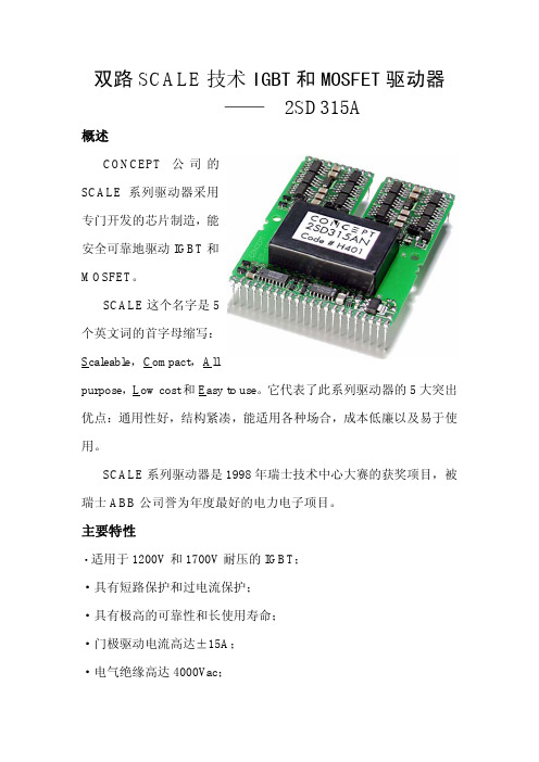
图 5 C 极采样电压曲线
Rth 值 22k 27k 33k 39k 47k
反应时间 ≈4.9us ≈5.7us ≈6.8us ≈7.6us ≈9us
Vth1 ≈4.8V ≈5.6V ≈6.5V ≈7.3V ≈8.4V
Vth2 ≈3.2V ≈3.9V ≈4.7V ≈5.6V ≈6.8V
测试条件 到 Ex
最小值 0
典型值
最大值 VDD
单位 Vdc
电气绝缘 输入输出隔离电压 耐压(50Hz/1min) 局部放电 输入输出爬电距离 输出间爬电距离 最大 dv/dt
测试条件 连续(注 8) 输入脚和输出脚间 IEC270(注 11)
△V=1000V(注 9)
最小值 100
典型值
>1700 20 12.7/20
G2
第 2 路驱动的 G
+15V
极
14
VDC
内置 DC/DC 变换器输入 31
G2
第 2 路驱动的 G
+15V
极
15
VDC
内置 DC/DC 变换器输入 30
COM2
第 2 路驱动电路
+15V
的公共地
16
VDC
内置 DC/DC 变换器输入 29
COM2
第 2 路驱动电路
+15V
的公共地
17
VDC
内置 DC/DC 变换器输入 28
双路 SCALE 技术 IGBT 和 MOSFET 驱动器 —— 2SD315A
概述
CONCEPT 公 司 的 SCALE 系列驱动器采用 专门开发的芯片制造,能 安全可靠地驱动 IGBT 和 MOSFET。
2SD717中文资料
Tel:(852)2341 9276 Fax:(852)2797 8153 E-mail: wsccltd@
TYP 70 50 10 3Fra bibliotek0 0.3 2.5 0.4
MAX 0.2 0.2 3 240 -
UNIT mA mA V V MHz pF us us us
Wing Shing Computer Components Co., (H.K.)Ltd. Homepage:
PARAMETER Collector-base cut-off current Emitter-base cut-off current Collector-emitter breakdown voltage Collector-emitter saturation voltages DC current gain Transition frequency at f = 5MHz Collector capacitance at f = 1MHz On times Tum-off storage time Fall time
Tmb 25 IC = 4.0A; IB=0.4A IF = 3.5A IC=4A,IB1=-IB2=0.4A,VCC=30V
1.5 0.4
LIMITING VALUES
SYMBOL
VCESM VCEO VEBO IC IB Ptot Tstg Tj
PARAMETER Collector-emitter voltage peak value Collector-emitter voltage (open base) Emitter-base oltage (open colloctor) Collector current (DC) Base current (DC) Total power dissipation Storage temperature Junction temperature
2SD315AI 中文版
典型值 11.5 0.7
最大值
单位 Vdc Vdc
逻辑电平输入 测试条件
最小值 典型值
输入电压
所有输入脚(注 4) 0
最大值 VDD
单位 Vdc
响应时间 输出延迟
封锁时间
测试条件
最小值
开通 tpd(on)
关断 tpd(off)
故障发生后(注 14)
典型值 300 350 1
最大值
单位 ns ns s
空载
30
mA
最大电源电流 IDC (注 2)
470
mA
DC/DC 变换器功率 (注 3)
6
W
效率
内置 DC/DC 变换器
85
%
VDD 电源输入
到 GND
15
Vdc
电源电流 IDD
空载
12
mA
电源电流 IDD
开关频率 25KHz
15
mA
电源监视 起动工作电压 电压滞环
测试条件 (注 4) (注 4)
最小值
功能定义 第 1 路驱动的 G 极 第 1 路驱动的 G 极 第 1 路驱动电路 的公共地 第 1 路驱动电路 的公共地 第 1 路驱动电路 的支撑电容
6
InB
第 1 路驱动信号输入
39
E1
第 1 路驱动的 E
极
7
RC2
外接 RC 生成第 2 路死区 38
E1
第 1 路驱动的 E
时间
极
8
MOD
模式选择输入
电气参数供电电源测试条件最小值典型值最大值单位vdc电源输入到gnd15vdc电源电流idc空载30ma最大电源电流idc470madcdc变换器功率效率内置dcdc变换器85vdd电源输入到gnd15vdc电源电流idd空载12ma电源电流idd开关频率25khz15ma电源监视测试条件最小值典型值最大值单位起动工作电压115vdc电压滞环07vdc逻辑电平输入测试条件最小值典型值最大值单位输入电压所有输入脚注4vddvdc响应时间测试条件最小值典型值最大值单位输出延迟开通tpdon关断tpdoff300350nsns封锁时间故障发生后注14输出测试条件最小值典型值最大值单位输出电流iggx到ex注61515上升时间troutgx到ex注6100160ns下降时间troutgx到ex注680130nssox输出电流15sox输出电压vddlsx输出电流mavce监测测试条件最小值典型值最大值单位cx输入到exvddvdc电气绝缘测试条件最小值典型值最大值单位输入输出隔离电压连续注81200vdc耐压50hz1min输入脚和输出脚间4000vac有效值局部放电iec270注111700vac峰值输入输出爬电距离20mm输出间爬电距离12720mm最大dvdtv1000v注9100kvus工作条件测试条件最小值典型值最大值单位工作温度2sd315ai注102sd315ai注10407085储存温度所有型号4090除非特别说明所有数据测试条件均为25环境温度及vddvdc15v注1
2SD2012(F,M);中文规格书,Datasheet资料
TOSHIBA Transistor Silicon NPN Triple Diffused Type2SD2012Audio Frequency Power Amplifier Applications• Low saturation voltage: V CE (sat) = 0.4 V (typ.) (I C = 2A / I B = 0.2A) • High power dissipation: P C = 25 W (Tc = 25°C)Absolute Maximum Ratings (Ta = 25°C)Characteristics Symbol Rating UnitCollector-base voltage V CBO 60 V Collector-emitter voltage V CEO 60 V Emitter-base voltage V EBO 7 V Collector current I C 3 A Base current I B 0.5 A Ta = 25°C 2.0 Collector powerdissipationTc = 25°CP C25WJunction temperature T j 150 °C Storage temperature rangeT stg−55 to 150°CNote 1: Using continuously under heavy loads (e.g. the application of hightemperature/current/voltage and the significant change in temperature, etc.) may cause this product to decrease in the reliability significantly even if the operating conditions (i.e.operating temperature/current/voltage, etc.) are within the absolute maximum ratings.Please design the appropriate reliability upon reviewing the Toshiba Semiconductor Reliability Handbook(“Handling Precautions”/Derating Concept and Methods) and individual reliability data (i.e. reliability test report and estimated failure rate, etc).Unit: mmJEDEC ― JEITA―TOSHIBA 2-10R1A Weight: 1.7 g (typ.)Electrical Characteristics (Ta = 25°C)Typ.Max UnitCondition Min Characteristics Symbol TestCollector cut-off current I CBO V CB = 60 V, I E = 0 ―― 100μA Emitter cut-off current I EBO V EB = 7 V, I C = 0 ―― 100μA Collector-emitter breakdown voltage V (BR) CEO I C = 50 mA, I B = 0 60 ―― Vh FE (1)V CE = 5 V, I C = 0.5 A 100 ― 320DC current gainh FE (2)V CE = 5 V, I C = 2 A 20 ――Collector-emitter saturation voltage V CE (sat)I C = 2 A, I B = 0.2 A ― 0.4 1.0 V Base-emitter voltage V BE V CE = 5 V, I C = 0.5 A ― 0.75 1.0 V Transition frequency f T V CE = 5 V, I C = 0.5 A ― 3 ― MHz Collector output capacitance C ob V CB = 10 V, I E = 0, f = 1 MHz ― 35 ― pF MarkingD2012Note 2: A line under a Lot No. identifies the indication of product Labels.Not underlined: [[Pb]]/INCLUDES > MCVUnderlined: [[G]]/RoHS COMPATIBLE or [[G]]/RoHS [[Pb]]Please contact your TOSHIBA sales representative for details as to environmental matters such as the RoHScompatibility of Product. The RoHS is the Directive 2002/95/EC of the European Parliament and of the Council of 27 January 2003 on the restriction of the use of certain hazardous substances in electrical and electronic equipment.Collector-emitter voltage V CE (V)I C – V CECo l le c t o r c u r r e n tI C (A )Collector current I C (A)h FE – ICD C c u r r e n t g a in h F ECollector current I C (A)V CE (sat) – I CC o l l e c t o r -e m i t t e r s a t u r a t io nv o l t a g e V C E (sa t ) (V )Base-emitter voltage V BE (V)I C – V BEC ol lect o rc u rr en tI C(A )Ambient temperature Ta (°C)P C – TaC o l l e c t o r p o w e r d i s s i p a t i o n P C (W )Collector-emitter voltage V CE (V)Safe Operating AreaC o l l e c t o r c u r r e n t I C (A )Pulse width t w (s)r th – t wT r a n s i e n t t h e r m a l r e s i s t a n c e r t h (°C /W )1 10 1000.10.010.001RESTRICTIONS ON PRODUCT USE•Toshiba Corporation, and its subsidiaries and affiliates (collectively “TOSHIBA”), reserve the right to make changes to the information in this document, and related hardware, software and systems (collectively “Product”) without notice.•This document and any information herein may not be reproduced without prior written permission from TOSHIBA. Even with TOSHIBA’s written permission, reproduction is permissible only if reproduction is without alteration/omission.•Though TOSHIBA works continually to improve Product’s quality and reliability, Product can malfunction or fail. Customers are responsible for complying with safety standards and for providing adequate designs and safeguards for their hardware, software and systems which minimize risk and avoid situations in which a malfunction or failure of Product could cause loss of human life, bodily injury or damage to property, including data loss or corruption. Before customers use the Product, create designs including the Product, or incorporate the Product into their own applications, customers must also refer to and comply with (a) the latest versions of all relevant TOSHIBA information, including without limitation, this document, the specifications, the data sheets and application notes for Product and the precautions and conditions set forth in the “TOSHIBA Semiconductor Reliability Handbook” and (b) theinstructions for the application with which the Product will be used with or for. Customers are solely responsible for all aspects of their own product design or applications, including but not limited to (a) determining the appropriateness of the use of this Product in such design or applications; (b) evaluating and determining the applicability of any information contained in this document, or in charts, diagrams, programs, algorithms, sample application circuits, or any other referenced documents; and (c) validating all operating parameters for such designs and applications. TOSHIBA ASSUMES NO LIABILITY FOR CUSTOMERS’ PRODUCT DESIGN OR APPLICATIONS.•Product is intended for use in general electronics applications (e.g., computers, personal equipment, office equipment, measuring equipment, industrial robots and home electronics appliances) or for specific applications as expressly stated in this document.Product is neither intended nor warranted for use in equipment or systems that require extraordinarily high levels of quality and/or reliability and/or a malfunction or failure of which may cause loss of human life, bodily injury, serious property damage or serious public impact (“Unintended Use”). Unintended Use includes, without limitation, equipment used in nuclear facilities, equipment used in the aerospace industry, medical equipment, equipment used for automobiles, trains, ships and other transportation, traffic signaling equipment, equipment used to control combustions or explosions, safety devices, elevators and escalators, devices related to electric power, and equipment used in finance-related fields. Do not use Product for Unintended Use unless specifically permitted in this document.•Do not disassemble, analyze, reverse-engineer, alter, modify, translate or copy Product, whether in whole or in part.•Product shall not be used for or incorporated into any products or systems whose manufacture, use, or sale is prohibited under any applicable laws or regulations.•The information contained herein is presented only as guidance for Product use. No responsibility is assumed by TOSHIBA for any infringement of patents or any other intellectual property rights of third parties that may result from the use of Product. No license to any intellectual property right is granted by this document, whether express or implied, by estoppel or otherwise.•ABSENT A WRITTEN SIGNED AGREEMENT, EXCEPT AS PROVIDED IN THE RELEVANT TERMS AND CONDITIONS OF SALE FOR PRODUCT, AND TO THE MAXIMUM EXTENT ALLOWABLE BY LAW, TOSHIBA (1) ASSUMES NO LIABILITYWHATSOEVER, INCLUDING WITHOUT LIMITATION, INDIRECT, CONSEQUENTIAL, SPECIAL, OR INCIDENTAL DAMAGES OR LOSS, INCLUDING WITHOUT LIMITATION, LOSS OF PROFITS, LOSS OF OPPORTUNITIES, BUSINESS INTERRUPTION AND LOSS OF DATA, AND (2) DISCLAIMS ANY AND ALL EXPRESS OR IMPLIED WARRANTIES AND CONDITIONS RELATED TO SALE, USE OF PRODUCT, OR INFORMATION, INCLUDING WARRANTIES OR CONDITIONS OF MERCHANTABILITY, FITNESS FOR A PARTICULAR PURPOSE, ACCURACY OF INFORMATION, OR NONINFRINGEMENT.•Do not use or otherwise make available Product or related software or technology for any military purposes, including without limitation, for the design, development, use, stockpiling or manufacturing of nuclear, chemical, or biological weapons or missile technology products (mass destruction weapons). Product and related software and technology may be controlled under the Japanese Foreign Exchange and Foreign Trade Law and the U.S. Export Administration Regulations. Export and re-export of Product or related software or technology are strictly prohibited except in compliance with all applicable export laws and regulations. •Please contact your TOSHIBA sales representative for details as to environmental matters such as the RoHS compatibility of Product.Please use Product in compliance with all applicable laws and regulations that regulate the inclusion or use of controlled substances, including without limitation, the EU RoHS Directive. TOSHIBA assumes no liability for damages or losses occurring as a result of noncompliance with applicable laws and regulations.分销商库存信息: TOSHIBA2SD2012(F,M)。
- 1、下载文档前请自行甄别文档内容的完整性,平台不提供额外的编辑、内容补充、找答案等附加服务。
- 2、"仅部分预览"的文档,不可在线预览部分如存在完整性等问题,可反馈申请退款(可完整预览的文档不适用该条件!)。
- 3、如文档侵犯您的权益,请联系客服反馈,我们会尽快为您处理(人工客服工作时间:9:00-18:30)。
2SD2074
IC — VCE
Collector to emitter saturation voltage VCE(sat) (V)
100 30 10 3 1 0.3 0.1 0.03 0.01 0.01 0.03 Ta=75˚C 25˚C –25˚C
VCE(sat) — IC
IC/IB=25
Collector power dissipation PC (W)
25˚C
200
0.1
0.3
1
3
10
0 0.01 0.03
0.1
0 –1
–3
–10
–30
–100
Collector current IC (A)
Collector current IC (A)
Emitter current IE (mA)
Cob — VCB
24
Ron — IB
IE=0 f=1MHz Ta=25˚C 1000 300 Ron measuring circuit IB=1mA
1:Emitter 2:Collector 3:Base MT2 Type Package
Printed circuit board: Copper foil area of 1cm2 or more, and the board thickness of 1.7mm for the collector portion
0.65 max.
1.0 1.0
s Features
0.2
Unit nA V V V
25 20 12 200 60 0.13 0.4 1.2 200 10 1.0 800
V V MHz pF Ω
Measurement circuit
1kΩ
*2
Pulse measurement
*1h
FE1
Rank classification
Base current IB (mA)
2
R 200 ~ 350 S 300 ~ 500 T 400 ~ 800
IB=1mA f=1kHz V=0.3V
Rank hFE1
VB
VV
VA
VB Ron= !1000(Ω) VA–VB
1
元器件交易网
Transistor
PC — Ta
1.2 1.2 Printed circut board: Copper foil area of 1cm2 or more, and the board thickness of 1.7mm for the collector portion. IB=4.0mA 1.0 Ta=25˚C 3.5mA 3.0mA 0.8 2.5mA 2.0mA 0.6 1.5mA 0.4 1.0mA 0.5mA 0.2
*
Symbol VCBO VCEO VEBO ICP IC PC Tj Tstg
Ratings 25 20 12 1 0.5 1 150 –55 ~ +150
Unit V V V A A W ˚C ˚C
0.45+0.1 – 0.05 1.2±0.1 0.65 max.
Note: In addition to the lead type shown in the upper figure, the type as shown in the lower figure is also available.
2.5±0.1
s Absolute Maximum Ratings
(Ta=25˚C)
1
(HW type)
s Electrical Characteristics
Parameter Collector cutoff current Collector to base voltage Collector to emitter voltage Emitter to base voltage Forward current transfer ratio Collector to emitter saturation voltage Base to emitter saturation voltage Transition frequency Collector output capacitance ON resistanse
VBE(sat) — IC
100
hFE — IC
IC/IB=10 1200 VCE=2V 400
fT — I E
VCB=10V Ta=25˚C
Base to emitter saturation voltage VBE(sat) (V)
1000
Transition frequency fT (MHz)
元器件交易网
Transistor
2SD2074
Silicon NPN epitaxial planer type
For low-frequency output amplification For muting For DC-DC converter
Unit: mm
6.9±0.1
(Ta=25˚C)
Symbol ICBO VCBO VCEO VEBO hFE1*1 hFE2 VCE(sat) VBE(sat) fT Cob Ron*3
*3R on
Conditions VCB = 25V, IE = 0 IC = 10µA, IE = 0 IC = 1mA, IB = 0 IE = 10µA, IC = 0 VCE = 2V, IC = 0.5A*2 VCE = 2V, IC = 1A*2 IC = 0.5A, IB = 20mA IC = 0.5A, IB = 50mA VCB = 10V, IE = –50mA, f = 200MHz VCB = 10V, IE = 0, f= 1MHz
Collector output capacitance Cob (pF)
20
ON resistance Ron (Ω)
100 30 10 3 1 0.3
VB
V
VA
16
f=1kHz V=0.3V
12
8
4
0 1 3 10 30 100
0.1 0.01 0.030.1来自0.313
10
Collector to base voltage VCB (V)
1.0
0.8
0.6
0.4
0.2
0 0 40 80 120 160 200
Collector current IC (A)
0 0 1 2 3 4 5 6
0.1
0.3
1
3
10
Ambient temperature Ta (˚C)
Collector to emitter voltage VCE (V)
Collector current IC (A)
0.3 1 3 10
30 10 3 1 0.3 0.1 0.03 0.01 0.01 0.03 Ta=–25˚C 75˚C
Forward current transfer ratio hFE
350 300 250 200 150 100 50
800 Ta=75˚C 600 25˚C –25˚C 400
min
typ
max 100
14.5±0.5
q
Low collector to emitter saturation voltage VCE(sat). Low ON resistance Ron. High foward current transfer ratio hFE. Allowing supply with the radial taping.
0.15
1.05 2.5±0.1 ±0.05
(1.45) 0.8
0.5 4.5±0.1
0.7
4.0
q q q
0.45–0.05
0.45–0.05
+0.1
+0.1
2.5±0.5
2.5±0.5 2 3
Parameter Collector to base voltage Collector to emitter voltage Emitter to base voltage Peak collector current Collector current Collector power dissipation Junction temperature Storage temperature