MY1B16G-450A资料下载
LM13700MNOPB,LM13700NNOPB,LM13700MXNOPB, 规格书,Datasheet 资料
LM13700LM13700 Dual Operational Transconductance Amplifiers with Linearizing Diodes and BuffersLiterature Number: SNOSBW2D芯天下--/LM13700Dual Operational Transconductance Amplifiers with Linearizing Diodes and BuffersGeneral DescriptionThe LM13700series consists of two current controlled transconductance amplifiers,each with differential inputs and a push-pull output.The two amplifiers share common supplies but otherwise operate independently.Linearizing diodes are provided at the inputs to reduce distortion and allow higher input levels.The result is a 10dB signal-to-noise improvement referenced to 0.5percent THD.High impedance buffers are provided which are especially de-signed to complement the dynamic range of the amplifiers.The output buffers of the LM13700differ from those of the LM13600in that their input bias currents (and hence their output DC levels)are independent of I ABC .This may result in performance superior to that of the LM13600in audio appli-cations.Featuresn g m adjustable over 6decades n Excellent g m linearityn Excellent matching between amplifiers n Linearizing diodesn High impedance buffersnHigh output signal-to-noise ratioApplicationsn Current-controlled amplifiers n Current-controlled impedances n Current-controlled filtersn Current-controlled oscillators n Multiplexers n TimersnSample-and-hold circuitsConnection DiagramDual-In-Line and Small Outline Packages00798102Top ViewOrder Number LM13700M,LM13700MX or LM13700NSee NS Package Number M16A or N16AJune 2004LM13700Dual Operational Transconductance Amplifiers with Linearizing Diodes and Buffers©2004National Semiconductor Corporation Absolute Maximum Ratings (Note 1)If Military/Aerospace specified devices are required,please contact the National Semiconductor Sales Office/Distributors for availability and specifications.Supply Voltage LM1370036V DC or ±18VPower Dissipation (Note 2)T A =25˚C LM13700N570mWDifferential Input Voltage ±5VDiode Bias Current (I D )2mA Amplifier Bias Current (I ABC )2mA Output Short Circuit DurationContinuousBuffer Output Current (Note 3)20mA Operating Temperature Range LM13700N 0˚C to +70˚C DC Input Voltage+V S to −V SStorage Temperature Range −65˚C to +150˚CSoldering Information Dual-In-Line Package Soldering (10sec.)260˚C Small Outline Package Vapor Phase (60sec.)215˚C Infrared (15sec.)220˚CElectrical Characteristics (Note 4)ParameterConditionsLM13700Units MinTyp Max Input Offset Voltage (V OS )Over Specified Temperature Range 0.44mV I ABC =5µA0.34V OS Including Diodes Diode Bias Current (I D )=500µA 0.55mV Input Offset Change 5µA ≤I ABC ≤500µA0.13mV Input Offset Current 0.10.6µA Input Bias Current Over Specified Temperature Range0.45µA18Forward6700960013000µmho Transconductance (g m )Over Specified Temperature Range 5400g m Tracking 0.3dBPeak Output CurrentR L =0,I ABC =5µA 5R L =0,I ABC =500µA350500650µA R L =0,Over Specified Temp Range300Peak Output Voltage Positive R L =∞,5µA ≤I ABC ≤500µA +12+14.2V Negative R L =∞,5µA ≤I ABC ≤500µA −12−14.4V Supply Current I ABC =500µA,Both Channels2.6mAV OS Sensitivity Positive ∆V OS /∆V +20150µV/V Negative ∆V OS /∆V −20150µV/V CMRR80110dB Common Mode Range ±12±13.5V CrosstalkReferred to Input (Note 5)100dB20Hz <f <20kHz Differential Input Current I ABC =0,Input =±4V0.02100nA Leakage Current I ABC =0(Refer to Test Circuit)0.2100nA Input Resistance 1026k ΩOpen Loop Bandwidth 2MHz Slew RateUnity Gain Compensated 50V/µs Buffer Input Current (Note 5)0.52µA Peak Buffer Output Voltage(Note 5)10VNote 1:“Absolute Maximum Ratings”indicate limits beyond which damage to the device may occur.Operating Ratings indicate conditions for which the device is functional,but do not guarantee specific performance limits.Note 2:For operation at ambient temperatures above 25˚C,the device must be derated based on a 150˚C maximum junction temperature and a thermal resistance,junction to ambient,as follows:LM13700N,90˚C/W;LM13700M,110˚C/W.Note 3:Buffer output current should be limited so as to not exceed package dissipation.L M 13700 2Electrical Characteristics (Note 4)(Continued)Note 4:These specifications apply for V S =±15V,T A =25˚C,amplifier bias current (I ABC )=500µA,pins 2and 15open unless otherwise specified.The inputs to the buffers are grounded and outputs are open.Note 5:These specifications apply for V S =±15V,I ABC =500µA,R OUT =5k Ωconnected from the buffer output to −V S and the input of the buffer is connected to the transconductance amplifier output.Schematic DiagramOne Operational Transconductance Amplifier00798101Typical Application00798118Voltage Controlled Low-Pass FilterLM137003Typical Performance CharacteristicsInput Offset Voltage Input Offset Current0079813800798139 Input Bias Current Peak Output Current0079814000798141 Peak Output Voltage andCommon Mode Range Leakage Current0079814200798143 LM1374Typical Performance Characteristics(Continued)Input LeakageTransconductance0079814400798145Input ResistanceAmplifier Bias Voltage vs.Amplifier Bias Current0079814600798147Input and Output Capacitance Output Resistance0079814800798149LM137005Typical Performance Characteristics(Continued)Distortion vs.DifferentialInput VoltageVoltage vs.AmplifierBias Current0079815000798151Output Noise vs.Frequency00798152Unity Gain Follower00798105L M 13700 6Typical Performance Characteristics(Continued)Leakage Current Test Circuit Differential Input Current Test Circuit0079810600798107Circuit DescriptionThe differential transistor pair Q4and Q5form a transcon-ductance stage in that the ratio of their collector currents isdefined by the differential input voltage according to thetransfer function:(1)where V IN is the differential input voltage,kT/q is approxi-mately26mV at25˚C and I5and I4are the collector currentsof transistors Q5and Q4respectively.With the exception ofQ12and Q13,all transistors and diodes are identical in size.Transistors Q1and Q2with Diode D1form a current mirrorwhich forces the sum of currents I4and I5to equal I ABC:I4+I5=I ABC(2)where I ABC is the amplifier bias current applied to the gainpin.For small differential input voltages the ratio of I4and I5approaches unity and the Taylor series of the In function canbe approximated as:(3)(4)Collector currents I4and I5are not very useful by themselvesand it is necessary to subtract one current from the other.The remaining transistors and diodes form three currentmirrors that produce an output current equal to I5minus I4thus:(5)The term in brackets is then the transconductance of theamplifier and is proportional to I ABC.Linearizing DiodesFor differential voltages greater than a few millivolts,Equa-tion(3)becomes less valid and the transconductance be-comes increasingly nonlinear.Figure1demonstrates howthe internal diodes can linearize the transfer function of theamplifier.For convenience assume the diodes are biasedwith current sources and the input signal is in the form ofcurrent I S.Since the sum of I4and I5is I ABC and the differ-ence is I OUT,currents I4and I5can be written as follows:Since the diodes and the input transistors have identicalgeometries and are subject to similar voltages and tempera-tures,the following is true:(6)Notice that in deriving Equation(6)no approximations havebeen made and there are no temperature-dependent terms.The limitations are that the signal current not exceed I D/2and that the diodes be biased with currents.In practice,replacing the current sources with resistors will generateinsignificant errors.ApplicationsVoltage Controlled AmplifiersFigure2shows how the linearizing diodes can be used in avoltage-controlled amplifier.To understand the input biasing,it is best to consider the13kΩresistor as a current sourceand use a Thevenin equivalent circuit as shown in Figure3.This circuit is similar to Figure1and operates the same.Thepotentiometer in Figure2is adjusted to minimize the effectsof the control signal at the output.LM137007ApplicationsVoltage Controlled Amplifiers(Continued)For optimum signal-to-noise performance,I ABC should be as large as possible as shown by the Output Voltage vs.Ampli-fier Bias Current rger amplitudes of input signal also improve the S/N ratio.The linearizing diodes help here by allowing larger input signals for the same output distortion as shown by the Distortion vs.Differential Input Voltage graph.S/N may be optimized by adjusting the magnitude of the input signal via R IN (Figure 2)until the output distortion is below some desired level.The output voltage swing can then be set at any level by selecting R L .Although the noise contribution of the linearizing diodes is negligible relative to the contribution of the amplifier’s inter-nal transistors,I D should be as large as possible.This mini-mizes the dynamic junction resistance of the diodes (r e )and maximizes their linearizing action when balanced against R IN .A value of 1mA is recommended for I D unless the specific application demands otherwise.00798108FIGURE 1.Linearizing Diodes00798109FIGURE 2.Voltage Controlled AmplifierL M 13700 8ApplicationsVoltage Controlled Amplifiers(Continued)Stereo Volume ControlThe circuit of Figure4uses the excellent matching of the twoLM13700amplifiers to provide a Stereo Volume Control witha typical channel-to-channel gain tracking of0.3dB.R P isprovided to minimize the output offset voltage and may bereplaced with two510Ωresistors in AC-coupled applications.For the component values given,amplifier gain is derived forFigure2as being:If V C is derived from a second signal source then the circuitbecomes an amplitude modulator or two-quadrant multiplieras shown in Figure5,where:The constant term in the above equation may be cancelledby feeding I S x I D R C/2(V−+1.4V)into I O.The circuit ofFigure6adds R M to provide this current,resulting in afour-quadrant multiplier where R C is trimmed such that V O=0V for V IN2=0V.R M also serves as the load resistor for I O.00798110FIGURE3.Equivalent VCA Input CircuitLM137009Stereo Volume Control(Continued)00798111FIGURE 4.Stereo Volume Control00798112FIGURE 5.Amplitude ModulatorL M 13700Stereo Volume Control(Continued)Noting that the gain of the LM13700amplifier of Figure 3may be controlled by varying the linearizing diode current I D as well as by varying I ABC ,Figure 7shows an AGC Amplifier using this approach.As V O reaches a high enough amplitude (3V BE )to turn on the Darlington transistors and the lineariz-ing diodes,the increase in I D reduces the amplifier gain so as to hold V O at that level.Voltage Controlled ResistorsAn Operational Transconductance Amplifier (OTA)may be used to implement a Voltage Controlled Resistor as shown in Figure 8.A signal voltage applied at R X generates a V IN to the LM13700which is then multiplied by the g m of the amplifier to produce an output current,thus:where g m ≈19.2I ABC at 25˚C.Note that the attenuation of V O by R and R A is necessary to maintain V IN within the linear range of the LM13700input.Figure 9shows a similar VCR where the linearizing diodes are added,essentially improving the noise performance of the resistor.A floating VCR is shown in Figure 10,where each “end”of the “resistor”may be at any voltage within the output voltage range of the LM13700.00798113FIGURE 6.Four-Quadrant Multiplier00798114FIGURE 7.AGC AmplifierLM13700Voltage Controlled Resistors(Continued)Voltage Controlled FiltersOTA’s are extremely useful for implementing voltage con-trolled filters,with the LM13700having the advantage that the required buffers are included on the I.C.The VC Lo-Pass Filter of Figure 11performs as a unity-gain buffer amplifier at frequencies below cut-off,with the cut-off frequency being the point at which X C /g m equals the closed-loop gain of (R/R A ).At frequencies above cut-off the circuit provides a single RC roll-off (6dB per octave)of the input signal ampli-tude with a −3dB point defined by the given equation,whereg m is again 19.2x I ABC at room temperature.Figure 12shows a VC High-Pass Filter which operates in much the same manner,providing a single RC roll-off below the de-fined cut-off frequency.Additional amplifiers may be used to implement higher order filters as demonstrated by the two-pole Butterworth Lo-Pass Filter of Figure 13and the state variable filter of Figure 14.Due to the excellent g m tracking of the two amplifiers,these filters perform well over several decades of frequency.00798115FIGURE 8.Voltage Controlled Resistor,Single-Ended00798116FIGURE 9.Voltage Controlled Resistor with Linearizing DiodesL M 13700Voltage Controlled Filters(Continued)00798117FIGURE10.Floating Voltage Controlled Resistor00798118FIGURE11.Voltage Controlled Low-Pass Filter LM13700Voltage Controlled Filters(Continued)00798119FIGURE 12.Voltage Controlled Hi-Pass Filter00798120FIGURE 13.Voltage Controlled 2-Pole Butterworth Lo-Pass FilterL M 13700Voltage Controlled Filters(Continued)Voltage Controlled OscillatorsThe classic Triangular/Square Wave VCO of Figure15is one of a variety of Voltage Controlled Oscillators which may be built utilizing the LM13700.With the component values shown,this oscillator provides signals from200kHz to below 2Hz as I C is varied from1mA to10nA.The output amplitudes are set by I A x R A.Note that the peak differential input voltage must be less than5V to prevent zenering the inputs.A few modifications to this circuit produce the ramp/pulse VCO of Figure16.When V O2is high,I F is added to I C to increase amplifier A1’s bias current and thus to increase the charging rate of capacitor C.When V O2is low,I F goes to zero and the capacitor discharge current is set by I C.The VC Lo-Pass Filter of Figure11may be used to produce a high-quality sinusoidal VCO.The circuit of Figure16em-ploys two LM13700packages,with three of the amplifiers configured as lo-pass filters and the fourth as a limiter/ inverter.The circuit oscillates at the frequency at which the loop phase-shift is360˚or180˚for the inverter and60˚per filter stage.This VCO operates from5Hz to50kHz with less than1%THD.00798121FIGURE14.Voltage Controlled State Variable Filter LM13700Voltage Controlled Oscillators(Continued)00798122FIGURE 15.Triangular/Square-Wave VCO00798123FIGURE 16.Ramp/Pulse VCOL M 13700Voltage Controlled Oscillators(Continued)Additional ApplicationsFigure 19presents an interesting one-shot which draws no power supply current until it is triggered.A positive-going trigger pulse of at least 2V amplitude turns on the amplifier through R B and pulls the non-inverting input high.The am-plifier regenerates and latches its output high until capacitor C charges to the voltage level on the non-inverting input.The output then switches low,turning off the amplifier and dis-charging the capacitor.The capacitor discharge rate is speeded up by shorting the diode bias pin to the inverting input so that an additional discharge current flows through D I when the amplifier output switches low.A special feature of this timer is that the other amplifier,when biased from V O ,can perform another function and draw zero stand-by power as well.00798124FIGURE 17.Sinusoidal VCO00798125Figure 18shows how to build a VCO using one amplifier when the other amplifier is needed for another function.FIGURE 18.Single Amplifier VCOLM13700Additional Applications(Continued)The operation of the multiplexer of Figure 20is very straight-forward.When A1is turned on it holds V O equal to V IN1and when A2is supplied with bias current then it controls V O .C C and R C serve to stabilize the unity-gain configuration of amplifiers A1and A2.The maximum clock rate is limited to about 200kHz by the LM13700slew rate into 150pF when the (V IN1–V IN2)differential is at its maximum allowable value of 5V.The Phase-Locked Loop of Figure 21uses the four-quadrant multiplier of Figure 6and the VCO of Figure 18to produce a PLL with a ±5%hold-in range and an input sensitivity of about 300mV.00798126FIGURE 19.Zero Stand-By Power Timer00798127FIGURE 20.MultiplexerL M 13700Additional Applications(Continued)The Schmitt Trigger of Figure22uses the amplifier output current into R to set the hysteresis of the comparator;thus V H=2x R x I B.Varying I B will produce a Schmitt Trigger with variable hysteresis.Figure23shows a Tachometer or Frequency-to-Voltage con-verter.Whenever A1is toggled by a positive-going input,an amount of charge equal to(V H–V L)C t is sourced into C f and R t.This once per cycle charge is then balanced by the current of V O/R t.The maximum F IN is limited by the amount of time required to charge C t from V L to V H with a current of I B,where V L and V H represent the maximum low and maxi-mum high output voltage swing of the LM13700.D1is added to provide a discharge path for C t when A1switches low.The Peak Detector of Figure24uses A2to turn on A1 whenever V IN becomes more positive than V O.A1then charges storage capacitor C to hold V O equal to V IN PK. Pulling the output of A2low through D1serves to turn off A1 so that V O remains constant.00798128FIGURE21.Phase Lock Loop00798129 FIGURE22.Schmitt Trigger LM13700Additional Applications(Continued)The Ramp-and-Hold of Figure 26sources I B into capacitor C whenever the input to A1is brought high,giving a ramp-rate of about 1V/ms for the component values shown.The true-RMS converter of Figure 27is essentially an auto-matic gain control amplifier which adjusts its gain such that the AC power at the output of amplifier A1is constant.The output power of amplifier A1is monitored by squaring ampli-fier A2and the average compared to a reference voltage with amplifier A3.The output of A3provides bias current tothe diodes of A1to attenuate the input signal.Because the output power of A1is held constant,the RMS value is constant and the attenuation is directly proportional to the RMS value of the input voltage.The attenuation is also proportional to the diode bias current.Amplifier A4adjusts the ratio of currents through the diodes to be equal and therefore the voltage at the output of A4is proportional to the RMS value of the input voltage.The calibration potentiom-eter is set such that V O reads directly in RMS volts.00798130FIGURE 23.Tachometer00798131FIGURE 24.Peak Detector and Hold CircuitL M 13700 20Additional Applications(Continued)00798132FIGURE 25.Sample-Hold Circuit00798133FIGURE 26.Ramp and HoldLM1370021Additional Applications(Continued)The circuit of Figure28is a voltage reference of variableTemperature Coefficient.The100kΩpotentiometer adjuststhe output voltage which has a positive TC above1.2V,zeroTC at about 1.2V,and negative TC below 1.2V.This isaccomplished by balancing the TC of the A2transfer functionagainst the complementary TC of D1.The wide dynamic range of the LM13700allows easy controlof the output pulse width in the Pulse Width Modulator ofFigure29.For generating I ABC over a range of4to6decades ofcurrent,the system of Figure30provides a logarithmic cur-rent out for a linear voltage in.Since the closed-loop configuration ensures that the input toA2is held equal to0V,the output current of A1is equal toI3=−V C/R C.The differential voltage between Q1and Q2is attenuated bythe R1,R2network so that A1may be assumed to be oper-ating within its linear range.From Equation(5),the inputvoltage to A1is:The voltage on the base of Q1is thenThe ratio of the Q1and Q2collector currents is defined by:Combining and solving for I ABC yields:This logarithmic current can be used to bias the circuit ofFigure4to provide temperature independent stereo attenu-ation characteristic.00798134FIGURE27.True RMS ConverterLM13722Additional Applications(Continued)00798135FIGURE 28.Delta VBE Reference00798136FIGURE 29.Pulse Width ModulatorLM1370023Additional Applications(Continued)00798137FIGURE 30.Logarithmic Current SourceL M 13700 24Physical Dimensionsinches (millimeters)unless otherwise notedS.O.Package (M)Order Number LM13700M or LM13700MXNS Package Number M16AMolded Dual-In-Line Package (N)Order Number LM13700N NS Package Number N16ALM1370025NotesLIFE SUPPORT POLICYNATIONAL’S PRODUCTS ARE NOT AUTHORIZED FOR USE AS CRITICAL COMPONENTS IN LIFE SUPPORT DEVICES OR SYSTEMS WITHOUT THE EXPRESS WRITTEN APPROVAL OF THE PRESIDENT AND GENERAL COUNSEL OF NATIONAL SEMICONDUCTOR CORPORATION.As used herein:1.Life support devices or systems are devices or systems which,(a)are intended for surgical implant into the body,or (b)support or sustain life,and whose failure to perform when properly used in accordance with instructions for use provided in the labeling,can be reasonably expected to result in a significant injury to the user. 2.A critical component is any component of a life support device or system whose failure to perform can be reasonably expected to cause the failure of the life support device or system,or to affect its safety or effectiveness.BANNED SUBSTANCE COMPLIANCENational Semiconductor certifies that the products and packing materials meet the provisions of the Customer Products Stewardship Specification (CSP-9-111C2)and the Banned Substances and Materials of Interest Specification (CSP-9-111S2)and contain no ‘‘Banned Substances’’as defined in CSP-9-111S2.National Semiconductor Americas Customer Support CenterEmail:new.feedback@ Tel:1-800-272-9959National SemiconductorEurope Customer Support CenterFax:+49(0)180-5308586Email:europe.support@Deutsch Tel:+49(0)6995086208English Tel:+44(0)8702402171Français Tel:+33(0)141918790National Semiconductor Asia Pacific Customer Support CenterEmail:ap.support@National SemiconductorJapan Customer Support Center Fax:81-3-5639-7507Email:jpn.feedback@ Tel:81-3-5639-7560L M 13700D u a l O p e r a t i o n a l T r a n s c o n d u c t a n c e A m p l i f i e r s w i t h L i n e a r i z i n g D i o d e s a n d B u f f e r sNational does not assume any responsibility for use of any circuitry described,no circuit patent licenses are implied and National reserves the right at any time without notice to change said circuitry and specifications.IMPORTANT NOTICETexas Instruments Incorporated and its subsidiaries(TI)reserve the right to make corrections,modifications,enhancements,improvements, and other changes to its products and services at any time and to discontinue any product or service without notice.Customers should obtain the latest relevant information before placing orders and should verify that such information is current and complete.All products are sold subject to TI’s terms and conditions of sale supplied at the time of order acknowledgment.TI warrants performance of its hardware products to the specifications applicable at the time of sale in accordance with TI’s standard warranty.Testing and other quality control techniques are used to the extent TI deems necessary to support this warranty.Except where mandated by government requirements,testing of all parameters of each product is not necessarily performed.TI assumes no liability for applications assistance or customer product design.Customers are responsible for their products and applications using TI components.To minimize the risks associated with customer products and applications,customers should provide adequate design and operating safeguards.TI does not warrant or represent that any license,either express or implied,is granted under any TI patent right,copyright,mask work right, or other TI intellectual property right relating to any combination,machine,or process in which TI products or services are rmation published by TI regarding third-party products or services does not constitute a license from TI to use such products or services or a warranty or endorsement e of such information may require a license from a third party under the patents or other intellectual property of the third party,or a license from TI under the patents or other intellectual property of TI.Reproduction of TI information in TI data books or data sheets is permissible only if reproduction is without alteration and is accompanied by all associated warranties,conditions,limitations,and notices.Reproduction of this information with alteration is an unfair and deceptive business practice.TI is not responsible or liable for such altered rmation of third parties may be subject to additional restrictions.Resale of TI products or services with statements different from or beyond the parameters stated by TI for that product or service voids all express and any implied warranties for the associated TI product or service and is an unfair and deceptive business practice.TI is not responsible or liable for any such statements.TI products are not authorized for use in safety-critical applications(such as life support)where a failure of the TI product would reasonably be expected to cause severe personal injury or death,unless officers of the parties have executed an agreement specifically governing such use.Buyers represent that they have all necessary expertise in the safety and regulatory ramifications of their applications,and acknowledge and agree that they are solely responsible for all legal,regulatory and safety-related requirements concerning their products and any use of TI products in such safety-critical applications,notwithstanding any applications-related information or support that may be provided by TI.Further,Buyers must fully indemnify TI and its representatives against any damages arising out of the use of TI products in such safety-critical applications.TI products are neither designed nor intended for use in military/aerospace applications or environments unless the TI products are specifically designated by TI as military-grade or"enhanced plastic."Only products designated by TI as military-grade meet military specifications.Buyers acknowledge and agree that any such use of TI products which TI has not designated as military-grade is solely at the Buyer's risk,and that they are solely responsible for compliance with all legal and regulatory requirements in connection with such use. TI products are neither designed nor intended for use in automotive applications or environments unless the specific TI products are designated by TI as compliant with ISO/TS16949requirements.Buyers acknowledge and agree that,if they use any non-designated products in automotive applications,TI will not be responsible for any failure to meet such requirements.Following are URLs where you can obtain information on other Texas Instruments products and application solutions:Products ApplicationsAudio /audio Communications and Telecom /communicationsAmplifiers Computers and Peripherals /computersData Converters Consumer Electronics /consumer-appsDLP®Products Energy and Lighting /energyDSP Industrial /industrialClocks and Timers /clocks Medical /medicalInterface Security /securityLogic Space,Avionics and Defense /space-avionics-defense Power Mgmt Transportation and Automotive /automotiveMicrocontrollers Video and Imaging /videoRFID OMAP Mobile Processors /omapWireless Connectivity /wirelessconnectivityTI E2E Community Home Page Mailing Address:Texas Instruments,Post Office Box655303,Dallas,Texas75265Copyright©2011,Texas Instruments Incorporated。
负载电源模块
4BA00)SIMATICS7-1500/ET 200MP负载电源模块PM 70 W 120/230VAC (6EP1332-4BA00)设备手册Siemens AG Industry Sector Postfach 48 4890026 NÜRNBERG A5E31691548-AAⓅ 02/2013 本公司保留技术更改的权利 Copyright © Siemens AG 2013. 保留所有权利法律资讯 警告提示系统为了您的人身安全以及避免财产损失,必须注意本手册中的提示。
人身安全的提示用一个警告三角表示,仅与财产损失有关的提示不带警告三角。
警告提示根据危险等级由高到低如下表示。
危险表示如果不采取相应的小心措施,将会导致死亡或者严重的人身伤害。
警告表示如果不采取相应的小心措施,可能导致死亡或者严重的人身伤害。
小心表示如果不采取相应的小心措施,可能导致轻微的人身伤害。
注意表示如果不采取相应的小心措施,可能导致财产损失。
当出现多个危险等级的情况下,每次总是使用最高等级的警告提示。
如果在某个警告提示中带有警告可能导致人身伤害的警告三角,则可能在该警告提示中另外还附带有可能导致财产损失的警告。
合格的专业人员本文件所属的产品/系统只允许由符合各项工作要求的合格人员进行操作。
其操作必须遵照各自附带的文件说明,特别是其中的安全及警告提示。
由于具备相关培训及经验,合格人员可以察觉本产品/系统的风险,并避免可能的危险。
按规定使用Siemens 产品请注意下列说明:警告Siemens 产品只允许用于目录和相关技术文件中规定的使用情况。
如果要使用其他公司的产品和组件,必须得到 Siemens 推荐和允许。
正确的运输、储存、组装、装配、安装、调试、操作和维护是产品安全、正常运行的前提。
必须保证允许的环境条件。
必须注意相关文件中的提示。
商标所有带有标记符号 ® 的都是西门子股份有限公司的注册商标。
2019一建机电实务WORD版教材(好用)
一级建造师机电实务(教材)目录1H411000机电工程常用材料及工程设备 (9)1H411010机电工程常用材料 (10)1H411011常用金属材料的类型及应用 (10)1H411012常用非金属材料的类型及应用 (21)1H411013常用电气材料的类型及应用 (31)1H411020机电工程常用工程设备 (38)1H411021通用机械设备的分类和性能 (38)1H411022专用设备的分类和性能 (48)1H411023静置设备的分类和性能 (58)1H411024电气设备的分类和性能 (60)1H412000机电工程专业技术 (70)1H412010测量技术 (71)1H412011测量的方法 (71)1H412012测量的要求 (79)1H412013常用测量仪器的应用 (86)1H412020起重技术 (95)1H412021起重机械的使用要求 (95)1H412022吊具的选用原则 (103)1H412023常用吊装方案的选用原则 (109)1H412030焊接技术 (126)1H412031焊接材料与设备选用原则 (127)1H412032焊接方法与工艺评定 (139)1H412033焊接应力与焊接变形及其控制 (148)1H412034焊接质量检验方法 (156)1H413000工业机电工程安装技术 (166)1H413010机械设备安装技术 (166)1H413011机械设备基础的种类及验收要求 (167)1H413012机械设备安装程序 (172)1H413013机械设备安装的方法 (178)1H413014机械设备安装的精度控制要求 (189)1H413020电气工程安装技术 (198)1H413021成套配电装置的安装技术 (198)1H413022变压器的安装技术 (206)1H413023旋转电机的安装技术 (215)1H413024输配电线路的施工技术 (223)1H413025防雷与接地装置的安装要求 (237)1H413030管道工程施工技术 (247)1H413031工业管道施工程序 (248)1H413032工业管道施工的技术要求 (257)1H413033工业管道吹洗与试压的要求 (266)1H413034长输管道施工程序 (276)1H413040静置设备及金属结构安装技术 (286)1H413041塔器设备的安装技术 (287)1H413042金属储罐(柜)制作安装技术 (295)1H413043球形罐的安装技术 (305)1H413044金属结构制作安装技术 (314)1H413050动力设备安装技术 (322)1H413051汽轮发电机安装技术 (322)1H413052锅炉设备安装技术 (332)1H413060自动化仪表工程安装技术 (343)1H413061自动化仪表工程安装程序 (344)1H413062自动化仪表设备安装要求 (348)1H413063自动化仪表线路及管路安装要求 (356)1H413064自动化仪表的调试要求 (362)1H413070防腐蚀工程施工技术 (367)1H413071设备及管道防腐蚀材料的性能 (367)1H413072设备及管道防腐蚀工程施工方法 (377)1H413073设备及管道防腐蚀工程施工要求 (385)1H413080绝热工程施工技术 (393)1H413081设备及管道绝热结构材料的性能 (393)1H413082设备及管道绝热结构组成与要求 (404)1H413083设备及管道绝热工程的施工方法 (409)1H413090工业炉窑砌筑工程施工技术 (421)1H413091工业炉窑砌筑材料的种类及性能 (422)1H413092工业炉窑砌筑工程施工程序 (424)1H413093工业炉窑砌筑施工技术要求 (427)1H414000建筑机电工程安装技术 (439)1H414010建筑管道工程安装技术 (439)1H414011建筑管道工程施工程序 (439)1H414012建筑管道施工技术要求 (448)1H414020建筑电气工程安装技术 (461)1H414021建筑电气工程施工程序 (462)1H414022建筑电气工程施工技术要求 (465)1H414030通风与空调工程安装技术 (482)1H414031通风与空调工程施工程序 (482)1H414032通风与空调工程施工技术要求 (491)1H414033净化空调系统施工要求 (503)1H414040建筑智能化工程安装技术 (506)1H414041建筑智能化工程的组成及其功能 (506)1H414042建筑智能化工程的施工要求 (515)1H414043建筑智能化工程的调试检测要求 (527)1H414050电梯工程安装技术 (543)1H414051电梯工程的施工程序 (543)1H414052电梯工程安装要求 (550)1H414060消防工程安装技术 (564)1H414061消防工程的类别及其功能 (565)1H414062消防工程施工要求 (579)1H414063消防工程的验收程序 (590)1H420000机电工程项目施工管理 (598)1H420010机电工程项目及其建设程序 (599)1H420011机电工程项目的特点 (599)1H420012机电工程项目的组成 (607)1H420013机电工程项目的建设程序 (611)1H420020机电工程项目管理的任务 (620)1H420021设计阶段项目管理的任务 (620)1H420022采购阶段项目管理的任务 (622)1H420023施工阶段项目管理的任务 (626)1H420024试运行阶段项目管理的任务 (634)1H420030机电工程施工招标投标管理 (641)1H420031施工招标投标管理要求 (641)1H420032施工招标条件与程序 (647)1H420033施工投标条件与程序 (651)1H420040机电工程施工合同管理 (666)1H420041合同文本与履约 (666)1H420042总包与分包合同的实施 (672)1H420043合同风险防范 (675)1H420044合同的变更与终止 (678)1H420045施工索赔的应用 (682)1H420050机电工程设备采购管理 (697)1H420051设备采购工作程序 (697)1H420052设备采购文件的编制要求 (703)1H420053设备询价的工作程序 (706)1H420054设备监造管理的要求 (711)1H420055设备检验要求 (717)1H420060机电工程施工组织设计 (729)1H420061施工组织设计的编制要求 (729)1H420062施工方案的编制要求 (736)1H420063施工组织设计的实施 (742)1H420064施工总平面图设计 (745)1H420070机电工程施工资源管理 (762)1H420071人力资源管理要求 (763)1H420072材料管理要求 (770)1H420073工程设备管理要求 (779)1H420074大型施工机械管理要求 (784)1H420075施工技术管理要求 (790)1H420076合理使用资金的要求 (800)1H420081施工现场内部协调管理实施 (817)1H420082施工现场外部协调管理实施 (820)1H420083对分包商的协调管理实施 (825)1H420090机电工程施工进度管理 (833)1H420091施工进度计划的编制要求 (834)1H420092施工进度控制的措施 (839)1H420093施工进度计划的调整 (841)1H420094费用一进度偏差分析 (845)1H420095费用-进度综合控制 (851)1H420100机电工程施工成本管理 (868)1H420101施工成本计划的编制要求 (868)1H420102施工成本计划的实施 (870)1H420103施工成本计划的分析 (873)1H420104施工成本控制的措施 (876)1H420110机电工程施工预结算 (885)1H420111施工图预算及定额的应用 (886)1H420112工程量清单计价的应用 (891)1H420113进度款支付与管理 (899)1H420114竣工结算规定的应用 (905)1H420120机电工程施工现场职业健康安全与环境管理 (917)1H420121风险管理策划 (918)1H420122应急预案实施要求 (928)1H420123职业健康和安全实施要求 (935)1H420124绿色施工实施要求 (946)1H420125文明施工实施要求 (957)1H420131施工质量控制的策划 (981)1H420132施工质量影响因素的预控 (987)1H420133施工质量检验的规定 (996)1H420134施工质量统计分析方法的应用 (1003)1H420135施工质量问题及事故分析处理 (1012)1H420140机电工程试运行管理 (1029)1H420141试运行应具备的条件 (1029)1H420142单体试运行管理要求 (1032)1H420143联动试运行管理要求 (1037)1H420144负荷试运行管理要求 (1041)1H420150机电工程竣工验收管理 (1050)1H420151竣工验收的依据 (1050)1H420152竣工验收的程序 (1056)1H420153竣工验收的内容 (1063)1H420160机电工程保修与回访管理 (1077)1H420161保修的职责 (1078)1H420162回访的实施 (1081)1H430000机电工程项目施工相关法规与标准 (1089)1H431000机电工程施工相关法规 (1089)1H431010计量法相关规定 (1089)1H431011计量器具的使用管理规定 (1090)1H431012计量检定的要求 (1105)1H431020电力法相关规定 (1112)1H431021用户用电的规定 (1112)1H431022电力设施保护区内施工作业的规定 (1123)1H431030特种设备安全法相关规定 (1136)1H431031特种设备的规定范围 (1137)1H431032特种设备制造、安装、改造的许可制度 (1146)1H431033特种设备的监督检验 (1155)1H432000机电工程施工相关标准 (1164)1H432010工业安装工程施工质量验收统一要求 (1164)1H432011工业安装工程施工质量验收的项目划分 (1165)1H432012工业安装工程分项工程质量验收评定 (1175)1H432013工业安装工程分部工程质量验收评定 (1178)1H432014工业安装工程单位工程质量验收评定 (1179)1H432020建筑安装工程施工质量验收统一要求 (1182)1H432021建筑安装工程施工质量验收的项目划分 (1183)1H432022建筑安装工程分项工程质量验收评定 (1190)1H432023建筑安装工程分部工程质量验收评定 (1195)1H432024建筑安装工程单位工程质量验收评定 (1197)1H433000一级建造师(机电工程)注册执业管理规定及相关要求 (1201)1H433001一级建造师(机电工程)注册执业工程规模标准 (1201)1H433002一级建造师(机电工程)注册执业工程范围 (1205)1H433003一级建造师(机电工程)施工管理签章文件目录 (1207)1H410000机电工程技术机电工程是指按照一定的工艺和方法,将不同规格、型号、性能、材质的设备、管路、线路等有机组合起来,满足使用功能要求的工程。
GB162BNYAAMLB-V01中文资料

JEWEL HILL ELECTRONIC CO.,LTDJEWEL HILL ELECTRONIC CO.,LTD.SPECIFICATIONS FORLCD MODULEModule No. GB162BOffice Address: Rm. 518,5/F., 101 Shangbu Industrial District,HuaqiangNorthRoad, Shenzhen, ChinaTEL : (86)-755-83362489 83617492FAX: (86)-755-83286396 83365871E-mail: sales@jhlcd@Website: TABLE OF CONTENTSLCM NUMBER SYSTEM (2)1. GENERAL DESCRIPTION (3)2. FEATURES (3)3. MECHANICAL SPECIFICATION (3)4. MECHANICAL DIMENSION (4)5. MAXIMUM RATINGS (5)6. ELECTRICAL CHARACTERISTICS (5)7. MODULE FUNCTION DESCRIPTION (6)8. ELECTRO-OPTICAL CHARACTERISTICS (12)9. RELIABILITY (16)10. PRECAUTIONS FOR USING LCD MODULES (17)11. USING LCD MODULES (19)12. REVISION HISTORY (21)SAMPLE APPROVED REPORT (22)LCM Number SystemNUMBER OF CHAR. PER LINE F: FSTN; X: OTHER VERSION NUMBER: V00~V99IC TYPE:VIEWING DIRECTION:TEMPERATURE RANGE:BACKLIGHT TYPE:SERIAL NUMBER: A~ZGRAPHIC MODULEs: NUMBER OF COMMONs GRAPHIC MODULEs:NUMBER OF SEGMENTs COB & SMT LCMBACKLIGHT COLOR:CHARACTER MODULEs:CHARACTER MODULEs: NUMBER OF LINE G: REFLECTIVE,NONE BACKLIGHT A: TRANSFLECTIVE, EL BACKLIGHT B: TRANSMISSIVE, EL BACKLIGHT C: TRANSFLECTIVE, LED BACKLIGHT D: TRANSMISSIVE, LED BACKLIGHT E: TRANSFLECTIVE, CCFL BACKLIGHT F: TRANSMISSIVE, CCFL BACKLIGHT A: AMBER; B: BLUE; Y: YELLOW-GREEN R: RED; W: WHITE; O: THER COLOR N: NORMAL TEMPERATURE RANGE U: UPPER(12:00); D: DOWN(6:00)L: LEFT(9:00); R: RIGHT(3:00);A: BONDING IC, WITH CONTROLLER B: BONDING IC, WITHOUT CONTROLLER C: SMT IC, WITH CONTROLLER D: SMT IC, WITHOUT CONTROLLER O: OTHER TYPEW: BLACK-WHITE; O: OTHER G: GRAY; Y: YELLOW-GREEN; B: BLUE; LCD COLOR MODE:N: TN; H: HTN; S: STN LCD TYPE:S: SUPER WIDE TEMPERATURE RANGE W: WIDE TEMPERATURE RANGEM: MIDDLE TEMPERATURE RANGE1. GENERAL DESCRIPTIONThe GB162B is a 16C x 2L Character LCD module. It has a STN panel composed of 80 segments and16 commons. The LCM can be easily accessed by micro-controller via parallel interface.2. FEATURESTransflective and positiveDisplay ModeSTN(Yellow - Green) moduleDisplay Format Character 16C x 2LInput Data 8/4-bit parallel data input from MPUMultiplexing Ratio 1/16 DutyBiasBias 1/5Viewing Direction 6 O’clockBacklight LED3. MECHANICAL SPECIFICATIONItem Specifications Unit Dimensional outline 122.0 x44.0 x 13.5(max) mmResolution 80segs x 16coms dotsActive area 94.84(W) x 20.0(H) mmChar. pitch 6.0(W) x 10.34(H) mmChar. size 4.84(W) x 9.66(H) mmDots pitch 0.98 (W)×1.16(H) mmDots size 0. 92(W)×1.1(H) mm4. MECHANICAL DIMENSION5. MAXIMUM RATINGSItem Symbol Min Max Unit NoteV DD - V ss -0.3 7.0 V Supply voltage V LCD -0.3 13.0 V Input Voltage V IN -0.3 V DD +0.3 VOperating temperature T OPR -10 +60 Storage temperature T STR -20 +70Humidity --- --- 90 %RH6. ELECTRICAL CHARACTERISTICSItem SymbolCondition Min. Typ. Max. UnitSupply Voltage Logic V DD------ 5.0 --- VH level V IH 0.8V DD --- V DDInput VoltageL levelV IL --- V SS --- 0.2V DDVCurrent Consumption(LCD DRIVER)I DDV DD =5.0V;V LCD =4.3V,T amb =25 ;--- --- 1.0 mALCD Driving Voltage V LCDBias=1/5V LCD =V DD -V O--- 4.3 --- VCurrent Consumption (With LED BackLight)I LEDV DD =5.0V;V LED =4.2V,T amb =25 ;--- --- 500 mA7. MODULE FUNCTION DESCRIPTION 7.1. PIN DESCRIPTIONPin No. Symbol Description1 VSSPower supply for Ground (0V)2 VDDPower supply for positive (+5V)3 VOLCD driver voltage regulation terminal4 RSData/Command register seletion; “H”: Data; “L”:Command5 R/WRead/write selection signal, ”H”: Read; ”L”: Write6 ERead/write Enable signal input pin7 DB08 DB19 DB210 DB38-bit bi-directional data bus11 DB412 DB513 DB614 DB715 LED+Power supply voltage for backlight positive16 LED-Power supply voltage for backlight negative7.2 TIMING CHARACTERISTICS1. SYSTEM BUS READ/WRITE CHARACTERISTIC7.3 APPLICATION OF LCMReference circuitCircuit Block Diagram7.4 TABLE OF COMMAND7.5 CHARACTER GENERATOR ROM8. ELECTRO-OPTICAL CHARACTERISTICSItem Symbol Condition Temp Min Typ. Max UnitsNote4.2 4.5 4.825 4.0 4.3 4.6 LCD driving voltageV LCD = = 050 3.8 4.1 4.4 V NOTE1Rise Time (Tr) --- --- -- Decay Time (Tf)0 --- ---- --- Rise Time (Tr) --- 225 340Decay Time (Tf) 25 --- 240 360Rise Time (Tr) --- --- -- Response TimeDecay Time (Tf)= = 0 50 --- --- --msec NOTE2Contrast Ratio Cr= = 0 255 10 --- --- NOTE4Viewing AngleRange( = 0°)(6”) = 90°(3”) =180°(12”) =270°(9”)(25 ) CR ≥245 30 15 30DegNOTE3z For panel only․Electro-Optical Characteristics Measuring Equipment(DMS501)SystemIllumination (D65)․Note 1. Definition of Driving Voltage( Vlcd) :․Note 3. Definition of Viewing Angle and :․Note 4. Definition of Contrast ratio( CR) :Brightness of Non-selected Segment (B2)Brightness of Selected Segment (B1)CR =V,maxCR,maxDriving VoltageB r ig h t n e s s (%)Brightness Curve forSelected Segment0%=90 =270Viewing Direction 6 O’clock DirectionNormal :9. RELIABILITY9.1. MTBFThe LCD module shall be designed to meet a minimum MTBF value of 50000 hours with normal. (25°C in the room without sunlight)9.2. TESTSNO. ITEM CONDITION CRITERION1 High Temperature Operating 60 120Hrs2 Low Temperature Operating -10 120Hrs3High Temperature/Humidity Non-Operating60 ,90%RH ,120 Hrs4 High TemperatureNon-Operating70 120Hrs5 Low TemperatureNon-Operating-20 120Hrs6 Temperature CyclingNon-Operating-10 (30Min )↔ 60 (30Min)10 CYCLESNo Defect OfOperational Function InRoom Temperature AreAllowable.IDD of LCM inPre-and post-test shouldfollow specificationNotes: Judgments should be mode after exposure in room temperature for two hours.10. PRECAUTIONS FOR USING LCD MODULES10.1. HANDLING PRECAUTIONS(1) The display panel is made of glass. Do not subject it to a mechanical shock or impact by droppingit.(2) If the display panel is damaged and the liquid crystal substance leaks out, be sure not to get any inyour mouth. If the substance contacts your skin or clothes, wash it off using soap and water.(3) Do not apply excessive force to the display surface or the adjoining areas since this may cause thecolor tone to vary.(4) The polarizer covering the display surface of the LCD module is soft and easily scratched. Handlethis polarizer carefully.(5) If the display surface becomes contaminated, breathe on the surface and gently wipe it with a softdry cloth. If it is heavily contaminated, moisten a cloth with one of the following solvents: - Isopropyl alcohol- Ethyl alcohol(6) Solvents other than those above mentioned may damage the polarizer.Especially, do not use the following:- Water- Ketone- Aromatic solvents(7) Extra care to minimize corrosion of the electrode. Water droplets, moisture condensation or acurrent flow in a high-humidity environment accelerates corrosion of the electrode.(8) Install the LCD Module by using the mounting holes. When mounting the LCD Module, makesure it is free of twisting, warping and distortion. In particular, do not forcibly pull or bend the I/Ocable or the backlight cable.(9) Do not attempt to disassemble or process the LCD Module.(10) NC terminal should be open. Do not connect anything.(11) If the logic circuit power is off, do not apply the input signals.(12) To prevent destruction of the elements by static electricity, be careful to maintain an optimumwork environment.- Be sure to ground the body when handling he LCD Module.- Tools required for assembling, such as soldering irons, must be properly grounded.-To reduce the amount of static electricity generated, do not conduct assembling and other workunder dry conditions.-The LCD Module is coated with a film to protect the display surface. Exercise care when peeling off this protective film since static electricity may be generated.10.2. STORAGE CONDITIONSWhen storing, avoid the LCD module to be exposed to direct sunlight of fluorescent lamps. For stability, to keep it away form high temperature and high humidity environment (The best condition is : 23±5°C, 45±20%RH). ESD protection is necessary for long-term storage also.10.3. OTHERSLiquid crystals solidify under low temperature (below the storage temperature range) leading to defective orientation or the generation of air bubbles (black or white). Air bubbles may also be generated if the module is subject to a low temperature.If the LCD Module have been operating for a long time showing the same display patterns the display patterns may remain on the screen as ghost images and a slight contrast irregularity may also appear.A normal operating status can be recovered by suspending use for some time. It should be noted that this phenomenon does not adversely affect performance reliability.To minimize the performance degradation of the LCD Module resulting from destruction caused by static electricity etc. exercise care to avoid holding the following sections when handling the modules.- Exposed area of the printed circuit board.- Terminal electrode sections.11. Using LCD modules11.1 LIQUID CRYSTAL DISPLAY MODULESLCD is composed of glass and polarizer. Pay attention to the following items when handling.(1) Please keep the temperature within specified range for use and storage. Polarization degradation,bubble generation or polarizer peel-off may occur with high temperature and high humidity.(2) Do not touch, push or rub the exposed polarizers with anything harder than a HB pencil lead (glass,tweezers, etc).(3) N-hexane is recommended for cleaning the adhesives used to attach front/rear polarizers andreflectors made of organic substances, which will be damaged by chemicals such as acetone, toluene, toluene, ethanol and isopropyl alcohol.(4) When the display surface becomes dusty, wipe gently with absorbent cotton or other soft materiallike chamois soaked in petroleum ether. Do not scrub hard to avoid damaging the display surface.(5) Wipe off saliva or water drops immediately, contact with water over a long period of time maycause deformation or color fading.(6) Avoid contacting oil and fats.(7) Condensation on the surface and contact with terminals due to cold will damage, stain orpolarizers. After products are tested at low temperature they must be warmed up in a container before coming is contacting with room temperature air.(8) Do not put or attach anything on the display area to avoid leaving marks on.(9) Do not touch the display with bare hands. This will stain the display area and degrade insulationbetween terminals (some cosmetics are determinate to the polarizers).(10)As glass is fragile, it tends to become or chipped during handling especially on the edges. Pleaseavoid dropping or jarring.11.2 INSTALLING LCD MODULEAttend to the following items when installing the LCM.(1) Cover the surface with a transparent protective plate to protect the polarizer and LC cell.(2) When assembling the LCM into other equipment, the spacer to the bit between the LCM and thefitting plate should have enough height to avoid causing stress to the module surface, refer to the individual specifications for measurements. The measurement tolerance should be ±0.1mm.11.3 ELECTRO-STATIC DISCHARGE CONTROLSince this module uses a CMOS LSI, the same careful attention should be paid for electrostatic discharge as for an ordinary CMOS IC.(1) Make certain that you are grounded when handing LCM.(2) Before removing LCM from its packing case or incorporating it into a set, be sure the module andyour body have the same electric potential.(3) When soldering the terminal of LCM, make certain the AC power source for the soldering irondoes not leak.(4) When using an electric screwdriver to attach LCM, the screwdriver should be of groundpotentiality to minimize as much as possible any transmission of electromagnetic waves produced sparks coming from the commutator of the motor.(5) As far as possible, make the electric potential of your work clothes and that of the workbenches tothe ground potential.(6) To reduce the generation of electro-static discharge, be careful that the air in the work is not toodried. A relative humidity of 50%-60% is recommended.11.4 PRECAUTIONS FOR OPERATION(1) Viewing angle varies with the change of liquid crystal driving voltage (Vo). Adjust Vo to showthe best contrast.(2) Driving the LCD in the voltage above the limit will shorten its lifetime.(3) Response time is greatly delayed at temperature below the operating temperature range. However,this does not mean the LCD will be out of the order. It will recover when it returns to the specified temperature range.(4) If the display area is pushed hard during operation, the display will become abnormal. However, itwill return to normal if it is turned off and then on.(5) Condensation on terminals can cause an electrochemical reaction disrupting the terminal circuit.Therefore, this product must be used and stored within the specified condition of 23±5°C, 45±20%RH.(6) When turning the power on, input each signal after the positive/negative voltage becomes stable.11.5 SAFETY(1) It is recommended to crush damaged or unnecessary LCDs into pieces and wash them off withsolvents such as acetone and ethanol, which should later be burned.(2) If any liquid leaks out of a damaged glass cell and comes in contact with the hands, wash offthoroughly with soap and water.12. REVISION HISTORYrecord Date Version Reviseversion 05-01-011.0 Original2.0 Change specification format 05-11-193.0 Change contact mode 06-07-27SAMPLE APPROVED REPORT。
MMBZ5250BLT3G中文资料
MMBZ5221BLT1 SeriesPreferred DeviceZener Voltage Regulators 225 mW SOT−23 Surface MountThis series of Zener diodes is offered in the convenient, surface mount plastic SOT−23 package. These devices are designed to provide voltage regulation with minimum space requirement. They are well suited for applications such as cellular phones, hand held portables, and high density PC boards.Features•Pb−Free Packages are Available•225 mW Rating on FR−4 or FR−5 Board•Zener V oltage Range − 2.4 V to 91 V•Package Designed for Optimal Automated Board Assembly •Small Package Size for High Density Applications•ESD Rating of Class 3 (>16 KV) per Human Body Model Mechanical CharacteristicsCASE:V oid-free, transfer-molded, thermosetting plastic case FINISH:Corrosion resistant finish, easily solderableMAXIMUM CASE TEMPERATURE FOR SOLDERING PURPOSES: 260°C for 10 SecondsPOLARITY:Cathode indicated by polarity bandFLAMMABILITY RATING:UL 94 V−0MAXIMUM RATINGSMaximum ratings are those values beyond which device damage can occur. Maximum ratings applied to the device are individual stress limit values (not normal operating conditions) and are not valid simultaneously. If these limits are exceeded, device functional operation is not implied, damage may occur and reliability may be affected.1.FR−5 = 1.0 X 0.75 X 0.62 in.2.Alumina = 0.4 X 0.3 X 0.024 in, 99.5% alumina.Devices listed in bold, italic are ON Semiconductor Preferred devices. Preferred devices are recommended choices for future use and best overall value.ELECTRICAL CHARACTERISTICS(Pinout: 1-Anode, 2-No Connection, 3-Cathode) (T A = 25°C unless otherwise noted, V= 0.95 V Max. @ I = 10 mA)ZNOTE:MMBZ5233BLT1, MMBZ5246BLT1, MMBZ5251BLT1, and MMBZ5252BLT1 Not Available in 10,000/Tape & Reel.V Z , T E M P E R A T U R E C O E F F I C I E N T (m V /C )°θV Z , NOMINAL ZENER VOLTAGE (V)− 3− 2−1012345678Figure 1. Temperature Coefficients (Temperature Range −55°C to +150°C)V Z , T E M P E R A T U R E C O E F F I C I E N T (m V /C)°θ100101V Z , NOMINAL ZENER VOLTAGE (V)Figure 2. Temperature Coefficients (Temperature Range −55°C to +150°C)V Z , NOMINAL ZENER VOLTAGEFigure 3. Effect of Zener Voltage onZener ImpedanceZ Z T , D Y N A M I C I M P E D A N C E ()Ω1000100101V F , FORWARD VOLTAGE (V)Figure 4. Typical Forward VoltageI F , F O R W A R D C U R R E N T (m A )1000100101C , C A P A C I T A N C E (p F )V Z , NOMINAL ZENER VOLTAGE (V)Figure 5. Typical Capacitance 1000100101V Z , ZENER VOLTAGE (V)1001010.10.01I Z , Z E NE R C U R R E N T (m A )V Z , ZENER VOLTAGE (V)1001010.10.01I R , L E A K A G E C U R R E N T (A )µV Z , NOMINAL ZENER VOLTAGE (V)Figure 6. Typical Leakage Current10001001010.10.010.0010.00010.00001I Z , Z E N E R C U R R E N T (m A )Figure 7. Zener Voltage versus Zener Current(V Z Up to 12 V)Figure 8. Zener Voltage versus Zener Current(12 V to 91 V)PACKAGE DIMENSIONSSOT−23 (TO−236)CASE 318−08ISSUE AJ*For additional information on our Pb−Free strategy and solderingdetails, please download the ON Semiconductor Soldering and Mounting Techniques Reference Manual, SOLDERRM/D.SOLDERING FOOTPRINT*ǒmm inchesǓSCALE 10:1STYLE 8:PIN 1.ANODE2.NO CONNECTION3.CATHODEON Semiconductor and are registered trademarks of Semiconductor Components Industries, LLC (SCILLC). SCILLC reserves the right to make changes without further notice to any products herein. SCILLC makes no warranty, representation or guarantee regarding the suitability of its products for any particular purpose, nor does SCILLC assume any liability arising out of the application or use of any product or circuit, and specifically disclaims any and all liability, including without limitation special, consequential or incidental damages.“Typical” parameters which may be provided in SCILLC data sheets and/or specifications can and do vary in different applications and actual performance may vary over time. All operating parameters, including “Typicals” must be validated for each customer application by customer’s technical experts. SCILLC does not convey any license under its patent rights nor the rights of others. SCILLC products are not designed, intended, or authorized for use as components in systems intended for surgical implant into the body, or other applications intended to support or sustain life, or for any other application in which the failure of the SCILLC product could create a situation where personal injury or death may occur. Should Buyer purchase or use SCILLC products for any such unintended or unauthorized application, Buyer shall indemnify and hold SCILLC and its officers, employees, subsidiaries, affiliates,and distributors harmless against all claims, costs, damages, and expenses, and reasonable attorney fees arising out of, directly or indirectly, any claim of personal injury or death associated with such unintended or unauthorized use, even if such claim alleges that SCILLC was negligent regarding the design or manufacture of the part. SCILLC is an Equal Opportunity/Affirmative Action Employer. This literature is subject to all applicable copyright laws and is not for resale in any manner.PUBLICATION ORDERING INFORMATION。
Y 系列三相异步电动机产品样本(南洋)
2. 噪声容差为+3dB A 3.防护等级为 IP44
b. The limits are permitted to increase 3 dB (A). c. Protection Class is IP44.
技术数据 Technical Data
同步转速 1000r/min 6 极 380V 50Hz
6.5
71
77
0.86
3.7
2.2
2.3
7.0
71
78
0.85
5.0
2.2
2.3
7.0
75
80.5 0.86
7.4
2.2
2.3
7.0
75
82
0.87 10.0
2.2
2.3
7.0
79
85.5 0.87 13.2
2.2
2.3
7.0
79
85.5 0.88 18.1
2.0
2.3
7.0
83
86.2 0.88 24.5
85.3 0.78 54.7
2.0
2.2
6.5
71
90
7.5 Y160M-6 17.0
970
86
0.78 73.9
2.0
2.0
6.5
75
130
11 Y160L-6 24.6
970
87
0.78 108.3
2.0
2.0
6.5
75
160
15 Y180L-6 31.5
970
89.5 0.81 147.8
1.8
Synchronous speed 1000 r/min (6-pole), 380V, 50Hz
BTA-450A中文说明书
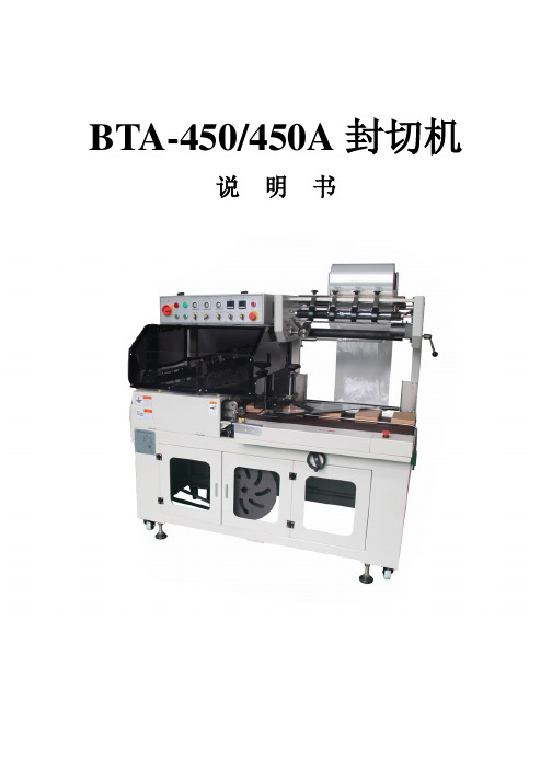
BTA-450/450A封切机说明书目录1. 安全注意事项 (1)2 .机械规格 (2)3.机械安装 (3)4.调试及操作 (5)5.机械调整 (12)6. 机械的保养 (17)7.故障排除 (20)8.电路图 (22)1.安全注意事项1.1一般安全注意事项:(1)操作人员操作本机前须详细阅读有关本机的各项使用操作说明,方可操作本机。
(2)为防止意外,操作本机时,应保持工作场所需通风良好,且应避免包装物破损而导致液体、气体外泄等情况发生。
(3)维修人员于维修保养本机时,需先详阅有关本机的维修说明,方可进行维修及保养工作。
(4)维修及保养时,务必先切断电源后,方可进行维修及保养工作。
(5)于机台运转后,若发生任何意外,必须先将电源关闭,然后作出相应措施。
(6)本机设计并不适合包装爆炸物品,如需包装小型物品、液体、粉状物件,需经箱型、罐形、包装袋等包装成型后,方可包装。
(7)本机台不适用于PVC材质之胶膜,因PVC材质容易损坏本机台之切刀寿命,若一定要使用PVC材质时,请特别注明,切刀必须为特别材质才能使用。
如果将PVC使用于POF切刀,其保修自动失效。
(8)本机未经授权而自行改装,发生任何危险恕不负责。
(9)如有任何问题,请与代理商联络。
(10)所有空压管路及气缸不能有油及水等污染物品,若有上述物体,其保修失效。
1.2特别注意事项:(1)非操作人员不可以随便操作机器。
机器在自动运行时,操作员不可以将手置于封口刀下面或电眼感应的范围内,以免造成安全事故。
(2)在机器压到产品报警或其他故障时,先按下急停开关,由自动运行选为手动运行,待清除故障后再松开急停开关,打回自动运行。
在清除封口刀下面的产品或拉膜时,按下急停开关后最好将安全门打开。
(3)电子胶布若裂开,必须更换,以免影响封口质量和封口刀的使用寿命。
封口刀上粘有胶膜或其他杂物时,需用棉毛巾擦干净。
清浩时,必须在手动下并将急停开关按下。
在做上述清洁时最好关掉总电源。
1937457资料

Dimensioned drawing
PHOENIX CONTACT GmbH & Co. KG http://www.phoenixcontact.de
Page 4 / 5 Mar 6, 2008
© 2008 Phoenix Contact Technical modifications reserved;
PHOENIX CONTACT GmbH & Co. KG http://www.phoenixcontact.de
Page 5 / 5 Mar 6, 2008
Page 1 / 5 Mar 6, 2008
元器件交易网
MCV 1,5/ 7-GF-3,5 THT Order No.: 1937457
http://eshop.phoenixcontact.de/phoenix/treeViewClick.do?UID=1937457
Drawings Application drawing
Drilling diagram
PHOENIX CONTACT GmbH & Co. KG http://www.phoenixcontact.de
Page 3 / 5 Mar 6, 2008
元器件交易网
MCV 1,5/ 7-GF-3,5 THT Order No.: 1937457
PHOENIX CONTACT GmbH & Co. KG http://www.phoenixcontact.de
Page 2 / 5 Mar 6, 2008
元器件交易网