ADL5320-EVALZ中文资料
AD5320中文资料
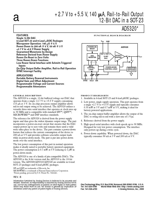
a
+2.7 V to +5.5 V, 140 A, Rail-to-Rail Output 12-Bit DAC in a SOT-23 AD5320*
FUNCTIONAL BLOCK DIAGRAM
VDD GND POWER-ON RESET
FEATURES Single 12-Bit DAC 6-Lead SOT-23 and 8-Lead SOIC Packages Micropower Operation: 140 A @ 5 V Power-Down to 200 nA @ 5 V, 50 nA @ 3 V +2.7 V to +5.5 V Power Supply Guaranteed Monotonic by Design Reference Derived from Power Supply Power-On-Reset to Zero Volts Three Power-Down Functions Low Power Serial Interface with Schmitt-Triggered Inputs On-Chip Output Buffer Amplifier, Rail-to-Rail Operation SYNC Interrupt Facility APPLICATIONS Portable Battery Powered Instruments Digital Gain and Offset Adjustment Programmable Voltage and Current Sources Programmable Attenuators
VDD 10
1/4 Scale to 3/4 Scale Change (400 Hex to C00 Hex). RL = 2 kΩ; 0 pF < CL < 200 pF. See Figure 16. RL = 2 kΩ; CL = 500 pF RL = ∞ RL = 2 k Ω 1 LSB Change Around Major Carry. See Figure 19.
FLUKE 5320A-LOAD 电气安全校准器 说明书

PN 3039085 February 2008 (Simplified Chinese) ©2008 Fluke Corporation. All rights reserved. Printed in USA.Specifications subject to change without notice.15320A-LOADHigh Voltage Load Adapter说明书简介5320A-LOAD High Voltage LoadAdapter (以下简称 Load )设设用于在使用 5320A电气安全测测校准器(以下简称“校准器”)校准高压测测压压压高压测测压压行加载以产生泄漏电流。
如图 1 所示,Load由一套八个额定功率电阻器组成,其配置可提供从 10 k Ω 至 5 M Ω的八种电阻抽头。
视所选电阻器而定,Load在设设上能够承受 1.2 kV 至 5.5 kV 的最大电压。
ehq059图 1. 负载示意图XW 警告为了避免可能发生的电电或人身伤害,只能按照本说明书或《5320A校准器用户手册》的规定使用本 Load 。
操作准备工作Load随机附带一个电源线适配器(用于驱驱冷却风扇)、一条接地电电和本说明书。
电源线适配器附带五个不同的电源插头适配器,以便与不同的电源插头配置相兼容。
使用之前,选选与本地电源插座匹配的适当插头适配器。
连接插头与电源线适配器之后,即可使用 Load 。
将 Load 置于校准器之上,在 Load后面板接地端子与校准器后面板接地端子之间连接接地电电。
XW 警告为了避免高压电能产生电电,确保将Load后部的接地端子接至校准器后部的接地 (GND)端子。
严禁在外壳未接地的情况下使用 Load 。
W 小心为了防止 Load 损坏,请确保 Load 底部的通风孔和风扇排气孔不被阻塞以保证冷却效果。
将电源线适配器的一端接至 Load后面板上配套的电源输入连接器插座,另一端接至电源插座。
ADL5542 RF IF增益模块说明书
ADI 中文版数据手册是英文版数据手册的译文,敬请谅解翻译中可能存在的语言组织或翻译错误,ADI 不对翻译中存在的差异或由此产生的错误负责。
如需确认任何词语的准确性,请参考ADI 提供的最新英文版数据手册。
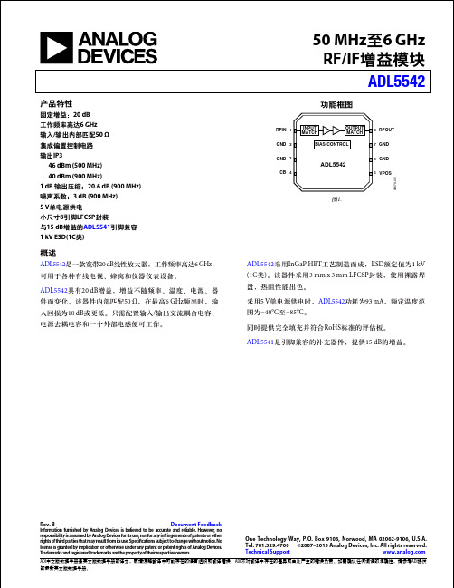
50 MHz 至6 GHz RF/IF 增益模块ADL5542Rev. BDocument Feedback Information furnished by Analog Devices is believed to be accurate and reliable. However , no responsibility is assumed by Analog Devices for its use, nor for any infringements of patents or other rights of third parties that may result from its use. Speci cations subject to change without notice. No license is granted by implication or otherwise under any patent or patent rights of Analog Devices. T rademarks and registered trademarks are the property of their respective owners.One Technology Way, P.O. Box 9106, Norwood, MA 02062-9106, U.S.A. Tel: 781.329.4700 ©2007–2013 Analog Devices, Inc. All rights reserved. Technical Support 功能框图2GND 7GND1RFIN 8RFOUT3GND 6GND4CB 5VPOSINPUT MATCHOUTPUT MATCHBIAS CONTROL ADL554206879-001图1.产品特性固定增益:20 dB 工作频率高达6 GHz 输入/输出内部匹配50 Ω集成偏置控制电路输出IP3 46 dBm (500 MHz)40 dBm (900 MHz)1 dB 输出压缩:20.6 dB (900 MHz)噪声系数:3 dB (900 MHz)5 V 单电源供电小尺寸8引脚LFCSP 封装与15 dB 增益的ADL5541引脚兼容1 kV ESD(1C 类)概述ADL5542是一款宽带20 dB 线性放大器,工作频率高达6 GHz ,可用于各种有线电视、蜂窝和仪器仪表设备。
手机模块SIM5320应用经验
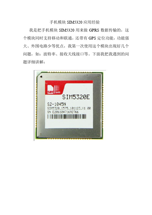
手机模块SIM5320应用经验
我是把手机模块SIM5320用来做GPRS数据传输的,这个模块同时支持移动和联通,还带有GPS定位功能,功能强大、外围电路少等优点,我第一次使用这个模块出现好几个问题,如:波特率、接收天线接口等。
下面我把我遇到的问题详细讲解:
1.模块SIM5320模块供电采用4.1V,如果单片机采用5V供电可以稳压4.8V用二极管1N4007降压
0.7V(4.8-0.7=4.1V),如果单片机采用3.3V供
电可以稳压4.0V用二极管1N4007降压0.7V(4.0
-0.7=3.3V)。
2.通讯可以直接使用RXD和TXD就可以了,但模块默认波特率是115200,如果需要更改波特率可以
发送更改波特率命令,但下次重启模块后又要重
新设置波特率。
模块的RXD和TXD接口电压是1.8V,
要做好接口电平转换问题。
3.接收天线接口:天线接口要求比较苛刻,处理不好直接影响模块工作,具体要求如下:
注:模块信号不好时会出现发指令不回复,或暂
时死机现象,等一阵子可能恢复正常。
4.模块控制采用AT+指令方式,详细可以参照SIM5320资料,这里就不详细讲解了。
5.工作原理图:。
ADL9005-EVALZ Evaluation Board User Guide

ADL9005-EVALZ Evaluation Board User GuideUG-1859One Technology Way • P .O. Box 9106 • Norwood, MA 02062-9106, U.S.A. • Tel: 781.329.4700 • Fax: 781.461.3113 • Evaluating the ADL9005 Wideband, Low Noise Amplifier, Single Positive Supply,0.01 GHz to 26.5 GHzPLEASE SEE THE LAST PAGE FOR AN IMPORTANT WARNING AND LEGAL TERMS AND CONDITIONS.Rev. 0 | Page 1 of 6FEATURES2-layer Rogers 4350B evaluation board with heat spreader End launch, 2.9 mm RF connectorsThrough calibration path (depopulated)EVALUATION KIT CONTENTSADL9005-EVALZ evaluation boardEQUIPMENT NEEDEDRF signal generator RF spectrum analyzer RF network analyzer5 V, 200 mA power supply External dc blockWideband, bias tee (Marki Microwave BT2-0040)GENERAL DESCRIPTIONThe ADL9005-EV AL Z consists of a 2-layer printed circuit board (PCB) fabricated from 10 mil thick, Rogers 4350B, copper clad, mounted to an aluminum heat spreader. The heat spreader assists in providing thermal relief to the device as well as mechanical support to the PCB. Mounting holes on the heat spreader allow attachment to larger heat s ink s for improved thermal management.The RFIN and RFOUT ports on the ADL9005-EV ALZ are populated with 2.9 mm, female coaxial connectors, and the respective RF traces have a 50 Ω characteristic impedance. The ADL9005-EV ALZ is populated with components suitable for use over the entire −40°C to +85°C operating temperature range of the ADL9005.To calibrate out board trace losses, a through calibration path, THRU CAL, is provided between the RFINTHRU and THRUCAL connectors. RFINTHRU and THRUCAL must be populated with RF connectors to use the through calibration path. The power voltages and ground path are accessed through surface-mounted technology (SMT) test points.An external wideband bias tee must be connected to RFOUT to provide bias current and ac coupling on RFOUT. The BT2-0040 from Marki Microwave is recommended.Alternatively, dc bias can be provided by connecting the dc supply voltage to the VDDOPT SMT test point.EVALUATION BOARD PHOTOGRAPHS24818-001Figure 1. ADL9005-EVALZ Top Side24818-002Figure 2. ADL9005-EVALZ Bottom SideThe RF traces are 50 Ω, grounded, coplanar waveguide. The package ground leads and the exposed pad directly connect to the ground plane. Multiple vias are used to connect the top and bottom ground planes with particular focus on the area directly beneath the ground pad to provide adequate electrical conduction and thermal conduction to the heat spreader.For full details on the ADL9005, see the ADL9005 data sheet, which must be consulted in conjunction with this user guide when using the ADL9005-EV ALZ.UG-1859ADL9005-EVALZ Evaluation Board User GuideRev. 0 | Page 2 of 6TABLE OF CONTENTSFeatures .............................................................................................. 1 Evaluation Kit Contents ................................................................... 1 Equipment Needed ........................................................................... 1 General Description ......................................................................... 1 Evaluation Board Photographs ....................................................... 1 Revision History ............................................................................... 2 Evaluation Board Hardware ............................................................ 3 Providing DC Bias Through a Connectorized Bias Tee ..............3 Providing DC Bias Through the ACG4/V DD2 Pin .........................3 Through Calibration Path ............................................................4 Evaluation Board Schematic and Artwork .....................................5 Ordering Information .......................................................................6 Bill of Materials (6)REVISION HISTORY2/2021—Revision 0: Initial VersionADL9005-EVALZ Evaluation Board User GuideUG-1859Rev. 0 | Page 3 of 6EVALUATION BOARD HARDWAREPROVIDING DC BIAS THROUGH A CONNECTORIZED BIAS TEEA 5 V , 200 mA supply is required to provide the bias to the ADL9005 when using the ADL9005-EV ALZ. Connect the 5 V supply through an external bias tee, such as the Marki Microwave BT2-0040, to the RFOUT port (see Figure 3). Connect the same 5 V supply to the VBIAS SMT test point. A connectorized dc blocking capacitor must be connected to the RFIN port because there is not an ac coupling capacitor on the RF input trace on the ADL9005-EV ALZ. The R1 value (default value is 300 Ω) sets the total current (I DQ ) to 80 mA.DC BLOCK24818-003Figure 3. ADL9005-EVALZ Operation Using a Connectorized Bias TeeRecommended Bias SequencingTo avoid damaging the device, careful attention must be paid to the sequencing of the RF input, the bias voltage, and the drain bias voltage. The following power-up sequencing is recommended: 1. Connect GND.2. Increase the voltage on the VBIAS SMT test point and theexternal bias tee to 5 V . 3. Apply the RF signal.The following power-down sequencing is recommended: 1. Turn off the RF signal.2. Reduce the voltage on the VBIAS SMT test point andthe external bias tee to 0 V .PROVIDING DC BIAS THROUGH THE ACG4/V DD2 PINAn alternative way to bias the ADL9005 when using the ADL9005-EV ALZ is by applying 8.5 V to the ACG4/V DD2 pin through the VDDOPT SMT test point and by applying 5 V to the R BIAS pin through the VBIAS SMT test point.The VDDOPT SMT test point connects directly to the ACG4/ V DD2 pin on the ADL9005. The higher 8.5 V supply is required to make up for the voltage drop across an internal resistor so that the internal drain bias voltage is still equal to 5 V . Applying this 8.5 V supply voltage to the VDDOPT SMT test point removes the need for an external bias tee, which must be replaced with a connectorized dc block on the RFOUT port (see Figure 4).With 5 V applied to the VBIAS SMT test point and the default value of R1 at 300 Ω, the resulting I DQ is 80 mA. The VBIAS SMT test point can also be connected directly to the 8.5 V supply. However, to do this, the R1 value must be increased to 850 Ω to maintain an I DQ of 80 mA.DC BLOCKDCBLOCK24818-004Figure 4. ADL9005-EVALZ Operation with V DD Applied Through theVDDOPT SMT Test PointRecommended Bias Sequencing when Providing Bias Through the VDDOPT SMT Test PointThe following sequencing is recommended for power-up when providing bias through the VDDOPT SMT test point: 1. Connect GND.2. Increase the voltage on the VDDOPT SMT test point to 8.5 V .3. Increase the voltage on the VBIAS SMT test point to 5 V .4.Apply the RF signal.The following sequencing is recommended for power-down when providing bias through the VDDOPT SMT test point: 1. Remove the RF signal.2. Decrease the voltage on the VBIAS SMT test point to 0 V .3. Decrease the voltage on the VDDOPT SMT test point to 0 V .UG-1859ADL9005-EVALZ Evaluation Board User GuideRev. 0 | Page 4 of 6THROUGH CALIBRATION PATHThe ADL9005-EV ALZ includes a calibration path (see the evaluation board schematic in Figure 6). RFINTHRU and THRUCAL must be populated with RF connectors to use the through calibration path. Figure 5 shows the insertion loss, input return loss and output return loss of the through calibration path.Table 1 lists the insertion loss of the through calibration path.FREQUENCY (GHz)246810121416182022242628–40–36–32–28–24–20–16–12–8–40I N S E R T I O N L O S S A N D R E T U R N L O S S (d B )24818-005Figure 5. Insertion Loss and Return Loss (Input and Output) of theThrough Calibration PathTable 1. Insertion Loss of the Through Calibration PathFrequency (GHz) Insertion Loss (dB) 0.01 +0.04 0.25 −0.013 0.5 −0.02 0.75 −0.023 1 −0.04 3 −0.1 5 −0.1 7 −0.2 9 −0.2 11 −0.3 13 −0.3 15 −0.5 17 −0.6 19 −0.5 21 −0.6 23 −0.7 25 −0.8 27−1.1ADL9005-EVALZ Evaluation Board User GuideUG-1859Rev. 0 | Page 5 of 624818-006Figure 6. ADL9005-EVALZ Schematic24818-007Figure 7. ADL9005-EVALZ Assembly Drawing (RFINTHRU and THRUCAL Not Installed)UG-1859ADL9005-EVALZ Evaluation Board User GuideRev. 0 | Page 6 of 6ORDERING INFORMATIONBILL OF MATERIALSTable 2.Reference Designator Description Manufacturer Manufacturer Number C1, C12 4.7 μF capacitors, tantalum, do not install (DNI) AVX TAJA475K020RNJ C2, C8 0.01 μF capacitors, ceramic, 0402, DNI KEMET C0402C103J3RACTU C4, C10 100 pF capacitors, ceramic, 0402 Samsung CL05C101JB5NNNC C5 100 pF capacitors, ceramic, 0402, DNI Samsung CL05C101JB5NNNC C6, C7 4.7 μF capacitors, tantalum AVX TAJA475K020RNJ C9, C11 0.01 μF capacitors, ceramic, 0402 KEMETC0402C103J3RACTU R1 300 Ω resistor, surface-mounted device (SMD), 0402 MULTICOMP (SPC) 0402WGF3000TCE R2, R3 0 Ω resistors, SMD, 0402, DNI PanasonicERJ-2GE0R00X RFINTHRU, THRUCAL Connectors, K jack edge, DNI SRI Connector Gage Co. 25-146-1000-92 VBIAS, VDDOPT, AGND Connectors, SMT test points Keystone Electronics 5016RFIN, RFOUT Connectors, K jack edge SRI Connector Gage Co. 25-146-1000-92 VGG2 Connectors, SMT test points, DNIKeystone Electronics 5016 U1Wideband, low noise amplifier, single positive supply, 0.01 GHz to 26.5 GHzAnalog Devices, Inc.ADL9005ESD CautionESD (electrostatic discharge) sensitive device . Charged devices and circuit boards can discharge without detection. Although this product features patented or proprietary protection circuitry, damage may occur on devices subjected to high energy ESD. Therefore, proper ESD precautions should be taken to avoid performance degradation or loss of functionality.Legal Terms and ConditionsBy using the evaluation board discussed herein (together with any tools, components documentation or support materials, the “Evaluation Board”), you are agreeing to be bound by the terms and conditions set forth below (“Agreement”) unless you have purchased the Evaluation Board, in which case the Analog Devices Standard Terms and Conditions of Sale shall govern. Do not use the Evaluation Board until you have read and agreed to the Agreement. Your use of the Evaluation Board shall signify your acceptance of the Agreement. This Agreement is made by and between you (“Customer”) and Analog Devices, Inc. (“ADI”), with its principal place of business at One Technology Way, Norwood, MA 02062, USA. Subject to the terms and conditions of the Agreement, ADI hereby grants to Customer a free, limited, personal, temporary, non-exclusive, non-sublicensable, non-transferable license to use the Evaluation Board FOR EVALUATION PURPOSES ONLY . Customer understands and agrees that the Evaluation Board is provided for the sole and exclusive purpose referenced above, and agrees not to use the Evaluation Board for any other purpose. Furthermore, the license granted is expressly made subject to the following additional limitations: Customer shall not (i) rent, lease, display, sell, transfer, assign, sublicense, or distribute the Evaluation Board; and (ii) permit any Third Party to access the Evaluation Board. As used herein, the term “Third Party” includes any entity other than ADI, Customer, their employees, affiliates and in-house consultants. The Evaluation Board is NOT sold to Customer; all rights not expressly granted herein, including ownership of the Evaluation Board, are reserved by ADI. CONFIDENTIALITY . This Agreement and the Evaluation Board shall all be considered the confidential and proprietary information of ADI. Customer may not disclose or transfer any portion of the Evaluation Board to any other party for any reason. Upon discontinuation of use of the Evaluation Board or termination of this Agreement, Customer agrees to promptly return the Evaluation Board to ADI. ADDITIONAL RESTRICTIONS. Customer may not disassemble, decompile or reverse engineer chips on the Evaluation Board. Customer shall inform ADI of any occurred damages or any modifications or alterations it makes to the Evaluation Board, including but not limited to soldering or any other activity that affects the material content of the Evaluation Board. Modifications to the Evaluation Board must comply with applicable law, including but not limited to the RoHS Directive. TERMINATION. ADI may terminate this Agreement at any time upon giving written notice to Customer. Customer agrees to return to ADI the Evaluation Board at that time. L IMITATION OF L IABIL ITY . THE EVALUATION BOARD PROVIDED HEREUNDER IS PROVIDED “AS IS” AND ADI MAKES NO WARRANTIES OR REPRESENTATIONS OF ANY KIND WITH RESPECT TO IT. ADI SPECIFICALLY DISCLAIMS ANY REPRESENTATIONS, ENDORSEMENTS, GUARANTEES, OR WARRANTIES, EXPRESS OR IMPLIED, RELATED TO THE EVALUATION BOARD INCLUDING, BUT NOT LIMITED TO, THE IMPL IED WARRANTY OF MERCHANTABILITY , TITL E, FITNESS FOR A PARTICUL AR PURPOSE OR NONINFRINGEMENT OF INTEL LECTUAL PROPERTY RIGHTS. IN NO EVENT WILL ADI AND ITS LICENSORS BE LIABLE FOR ANY INCIDENTAL, SPECIAL, INDIRECT, OR CONSEQUENTIAL DAMAGES RESULTING FROM CUSTOMER’S POSSESSION OR USE OF THE EVALUATION BOARD, INCLUDING BUT NOT LIMITED TO LOST PROFITS, DELAY COSTS, LABOR COSTS OR LOSS OF GOODWILL. ADI’S TOTAL LIABILITY FROM ANY AND ALL CAUSES SHALL BE LIMITED TO THE AMOUNT OF ONE HUNDRED US DOLLARS ($100.00). EXPORT. Customer agrees that it will not directly or indirectly export the Evaluation Board to another country, and that it will comply with all applicable United States federal laws and regulations relating to exports. GOVERNING LAW. This Agreement shall be governed by and construed in accordance with the substantive laws of the Commonwealth of Massachusetts (excluding conflict of law rules). Any legal action regarding this Agreement will be heard in the state or federal courts having jurisdiction in Suffolk County, Massachusetts, and Customer hereby submits to the personal jurisdiction and venue of such courts. The United Nations Convention on Contracts for the International Sale of Goods shall not apply to this Agreement and is expressly disclaimed. ©2021 Ana log Devices, Inc. All rights reserved. Tra dema rks a nd registered tra dema rks a re the property of their respective owners. UG24818-2/21(0)。
Circuits from the Lab

ADI 中文版数据手册是英文版数据手册的译文,敬请谅解翻译中可能存在的语言组织或翻译错误,ADI 不对翻译中存在的差异或由此产生的错误负责。
如需确认任何词语的准确性,请参考ADI 提供的最新英文版数据手册。
Circuits from the Lab™ reference circuits are engineered and tested for quick and easy system integration to help solve today’s analog, mixed-signal, and RF design challenges. For more information and/or support, visit /CN0248.ADRF6510 30 MHz 双通道可编程滤波器和可变增益放大器ADL5387 50 MHz 至2 GHz 正交解调器ADL5336集成48 dB 增益控制范围和可编程RMS 检波器的LF 至1 GHz VGA基于IQ 解调器,具有中频和基带可变增益以及可编程基带滤波功能的中频至基带接收机Rev. 0Circuits from the Lab™ circuits from Analog Devices have been designed and built by Analog Devices engineers. Standard engineering practices have been employed in the design and construction of each circuit, and their function and performance have been tested and veri ed in a lab environment at room temperature. However , you are solely responsible for testing the circuit and determining its suitability and applicability for your use and application. Accordingly , in no event shall Analog Devices be liable for direct, indirect, special, incidental, consequential or punitive damages due to any cause whatsoever connected to the use of any Circuits from the Lab circuits. (Continued on last page)One Technology Way, P.O. Box 9106, Norwood, MA 02062-9106, U.S.A. Tel: 781.329.4700 Fax: 781.461.3113 ©2012 Analog Devices, Inc. All rights reserved.ADRF6510IQRFDIV BY 2ADL53872xLO0°90°ADF4350ADL5336AD9248BITSBITS10285-001VCO CORE图1. 直接变频接收机原理示意图(所有连接和去耦均未显示)CN-0248电路笔记连接/参考器件评估和设计支持电路评估板ADRF6510评估板(ADRF6510-EVALZ)ADL5387评估板(ADL5387-EVALZ) ADL5336评估板(ADL5336-EVALZ) AD8130评估板(AD8130-EBZ),需要两个设计和集成文件原理图、布局文件、物料清单电路功能与优势该电路是灵活的频率捷变中频至基带接收机。
adl5315用法

adl5315用法ADL5315是一款电压模拟多功能数字电流表芯片,由美国Analog Devices(ADI)公司生产。
它主要用于电源管理、电源检测和电流测量等领域。
ADL5315拥有很多功能和优势,下面将详细介绍其使用方法。
1.ADL5315基本参数:-供电范围:2.7V至5.25V-电流测量范围:±200mA-分辨率:0.1mA-数字接口:I²C-工作温度范围:-40℃至+85℃2.ADL5315使用方法:ADL5315主要通过I²C接口与微处理器或其他数字电路进行通信。
以下是使用ADL5315的基本步骤:-步骤1:将ADL5315与待测试电路连接,确保电源和地线正确连接。
-步骤2:将ADL5315的SDA引脚连接至I²C总线的数据线上,将SCL引脚连接至I²C总线的时钟线上。
-步骤3:根据连接的电源电压范围选择合适的电源电压输出,接通电源。
-步骤4:使用相应的控制代码,通过I²C总线与ADL5315进行通信。
-步骤5:根据需要,读取和处理ADL5315返回的数据,如电流测量值、过温报警等。
3.ADL5315功能特点:ADL5315具有许多强大的功能和特点,以下是一些主要特点的介绍:-电压负载编程:可以根据需要设置电压负载,从而测试电路在不同负载下的电流表现。
-多通道输出:可同时测量多个电流值,并通过I²C接口输出给主控芯片,提高测试效率。
-精确度高:具备0.1mA的测量精度,可满足大部分电流测量需求。
-过温报警:当芯片温度超过预设阈值时,ADL5315会产生过温报警信号,以保护芯片免受过热损害。
-低功耗:在待机模式下,其功耗可以降低到无损耗水平,有助于延长电池寿命。
4.ADL5315应用领域:ADL5315广泛应用于各种电源管理、电源检测和电流测量的场合,特别适用于以下领域:-便携式设备:如智能手机、平板电脑、手持游戏机等,可用于电池管理和充电控制。
Analog Devices电路笔记 CN-0369参考设计说明书
Rev. 0Circuits from the Lab® reference designs from Analog Devices have been designed and built by Analog Devices engineers. Standard engineering practices have been employed in the design and construction of each circuit, and their function and performance have been tested and verified in a lab environment at room temperature. However, you are solely responsible for testing the circuit anddetermining its suitability and applicability for your use and application. Accordingly, in no event shall Analog Devices be liable for direct, indirect, special, incidental, consequential or punitive damages due to any cause whatsoever One Technology Way, P.O. Box 9106, Norwood, MA 02062-9106, U.S.A. Tel: /cn电路笔记CN-0369Circuits from the Lab®参考设计是经过测试的参考设计,有助于加速设计,同时简化系统集成,帮助并解决当今模拟、混合信号和RF设计挑战。
如需更多信息和/或技术支持,请访问/cn/CN0369。
- 1、下载文档前请自行甄别文档内容的完整性,平台不提供额外的编辑、内容补充、找答案等附加服务。
- 2、"仅部分预览"的文档,不可在线预览部分如存在完整性等问题,可反馈申请退款(可完整预览的文档不适用该条件!)。
- 3、如文档侵犯您的权益,请联系客服反馈,我们会尽快为您处理(人工客服工作时间:9:00-18:30)。
400 MHz to 2700 MHzRF Driver AmplifierADL5320 Rev. 0Information furnished by Analog Devices is believed to be accurate and reliable. However, noresponsibility is assumed by Analog Devices for its use, nor for any infringements of patents or other rights of third parties that may result from its use. Specifications subject to change without notice. No license is granted by implication or otherwise under any patent or patent rights of Analog Devices. T rademarks and registered trademarks are the property of their respective owners. O ne Technology Way, P.O. Box 9106, Norwood, MA 02062−9106, U.S.A. Tel: 781.329.4700 Fax: 781.461.3113 ©2008 Analog Devices, Inc. All rights reserved.FEATURESOperation: 400 MHz to 2700 MHz Gain of 17 dB at 880 MHzOIP3 of 45 dBm at 880 MHzP1dB of 25.4 dBm at 880 MHzNoise figure: 4 dB at 880 MHz Power supply: 5 VPower supply current: 104 mA typical Internal active biasingThermally efficient SOT-89 package ESD rating of ±4 kV (Class 3A) FUNCTIONAL BLOCK DIAGRAMIN OUT584Figure 1.GENERAL DESCRIPTIONThe ADL5320 is a broadband, linear driver RF amplifier that operates at frequencies from 400 MHz to 2700 MHz. The device can be used in a wide variety of wired and wireless applications, including ISM, WLL, PCS, GSM, CDMA, and W-CDMA.The ADL5320 operates with a 5 V supply voltage and a supply current of 104 mA. The ADL5320 is fabricated on a GaAs HBT process. The device is packaged in a low cost SOT-89 that uses an exposed paddle for excellent thermal impedance. It operates from −40°C to+85°C, and a fully populated evaluation board is available.ADL5320Rev. 0 | Page 2 of 16TABLE OF CONTENTSFeatures .............................................................................................. 1 Functional Block Diagram .............................................................. 1 General Description ......................................................................... 1 Revision History ............................................................................... 2 Specifications ..................................................................................... 3 Typical Scattering Parameters ..................................................... 4 Absolute Maximum Ratings ............................................................ 5 ESD Caution .................................................................................. 5 Pin Configuration and Function Descriptions .. (6)Typical Performance Characteristics ..............................................7 Basic Layout Connections ............................................................. 11 Soldering Information and Recommended PCB LandPattern .......................................................................................... 11 Matching Procedure ................................................................... 12 W-CDMA ACPR Performance ................................................ 13 Evaluation Board ............................................................................ 14 Outline Dimensions ....................................................................... 16 Ordering Guide .. (16)REVISION HISTORY2/08—Revision 0: Initial VersionADL5320Rev. 0 | Page 3 of 16SPECIFICATIONSVSUP = 5 V and T A = 25°C, unless otherwise noted. Table 1.ParameterConditions Min Typ Max Unit OVERALL FUNCTION Frequency Range 400 2700 MHz FREQUENCY = 880 MHzGain 116.3 16.9 17.5 dB vs. Frequency ±50 MHz ±0.3 dB vs. Temperature −40°C ≤ T A ≤ +85°C ±0.6 dB vs. Supply4.75 V to5.25 V ±0.1 dB Output 1 dB Compression Point 25.4 dBm Output Third-Order Intercept ∆f = 1 MHz, P OUT = 10 dBm per tone 45 dBm Noise Figure4.1 dB FREQUENCY = 2140 MHzGain 112.4 13.2 14.0 dB vs. Frequency ±50 MHz ±0.33 dB vs. Temperature −40°C ≤ T A ≤ +85°C ±0.8 dB vs. Supply4.75 V to5.25 V ±0.06 dB Output 1 dB Compression Point 25.7 dBm Output Third-Order Intercept ∆f = 1 MHz, P OUT = 10 dBm per tone 42 dBm Noise Figure4.4 dB FREQUENCY = 2600 MHzGain 111.5 12.5 13.4 dB vs. Frequency ±100 MHz ±0.6 dB vs. Temperature −40°C ≤ T A ≤ +85°C ±1.1 dB vs. Supply4.75 V to5.25 V ±0.1 dB Output 1 dB Compression Point 27.4 dBm Output Third-Order Intercept ∆f = 1 MHz, P OUT = 10 dBm per tone 37 dBm Noise Figure 5.1 dB POWER INTERFACE Pin RF OUT Supply Voltage 4.5 5 5.5 V Supply Current 104 124 mA vs. Temperature −40°C ≤ T A ≤ +85°C ±6.0 mA Power DissipationVSUP = 5 V 520 mW1Guaranteed maximum and minimum specified limits on this parameter are based on 6 sigma calculations.ADL5320Rev. 0 | Page 4 of 16TYPICAL SCATTERING PARAMETERSVSUP = 5 V and T A = 25°C; the effects of the test fixture have been de-embedded up to the pins of the device. Table 2.Freq (MHz) S11 S21 S12 S22Magnitude (dB) Angle (°) Magnitude (dB) Angle (°) Magnitude (dB) Angle (°) Magnitude (dB) Angle (°) 400 −1.51 164.18 14.18 +128.37 −32.37 +6.77 −3.44 160.94 500 −1.38 155.33 14.03 +118.16 −31.75 +1.48 −3.70 156.73 550 −1.42 151.34 13.79 +112.76 −31.68 −3.93 −3.79 154.66 600 −1.46 147.66 13.72 +108.71 −31.46 −4.60 −3.83 152.89 650 −1.46 144.12 13.53 +104.05 −31.56 −6.81 −3.90 151.08 700 −1.50 140.66 13.45 +98.89 −31.13 −9.87 −3.99 149.38 750 −1.56 137.19 13.21 +95.44 −31.12 −11.14 −4.02 147.87 800 −1.61 133.97 13.29 +90.33 −31.00 −13.96 −4.07 146.36 850 −1.66 130.74 13.04 +86.67 −30.60 −14.90 −4.12 144.94 900 −1.72 127.65 13.03 +81.59 −30.72 −17.78 −4.21 143.60 950 −1.85 124.15 12.92 +77.91 −30.31 −20.23 −4.25 142.41 1000 −1.92 120.90 12.93 +73.13 −30.22 −22.21 −4.27 141.31 1050 −2.02 117.54 12.92 +68.80 −29.98 −24.19 −4.32 140.51 1100 −2.20 114.21 12.76 +64.12 −29.80 −28.18 −4.37 139.63 1150 −2.41 110.72 12.97 +59.95 −29.39 −29.56 −4.43 138.68 1200 −2.62 107.22 12.69 +54.62 −29.46 −33.00 −4.42 138.09 1250 −2.87 103.77 12.98 +50.95 −29.03 −37.13 −4.47 137.74 1300 −3.16 99.97 12.87 +44.96 −28.75 −38.18 −4.44 137.08 1350 −3.65 96.51 12.94 +40.47 −28.81 −44.64 −4.45 136.77 1400 −4.09 92.23 12.87 +35.36 −28.26 −46.78 −4.40 136.49 1450 −4.59 88.76 13.04 +30.47 −28.43 −49.56 −4.37 136.43 1500 −5.28 84.62 13.00 +24.40 −28.13 −56.47 −4.29 135.79 1550 −6.09 80.71 12.89 +19.39 −27.96 −59.31 −4.20 135.63 1600 −6.98 77.02 13.13 +14.80 −27.98 −62.71 −4.05 135.39 1650 −8.06 72.69 13.07 +7.27 −27.73 −69.93 −3.88 134.43 1700 −9.38 68.92 13.00 +2.17 −27.49 −73.80 −3.71 133.76 1750 −11.15 66.21 12.97 −3.27 −27.78 −77.79 −3.59 132.94 1800 −13.20 63.18 13.18 −9.57 −27.23 −85.28 −3.29 131.04 1850 −15.83 63.73 13.03 −17.27 −27.36 −89.22 −3.11 129.62 1900 −19.87 71.29 12.84 −22.35 −27.40 −96.30 −2.93 127.46 1950 −24.51 103.69 13.08 −29.10 −27.26 −102.96 −2.69 124.63 2000 −22.66 156.61 12.86 −36.58 −27.33 −109.25 −2.54 122.53 2050 −18.02 171.65 12.88 −43.14 −27.33 −117.37 −2.50 118.78 2100 −14.34 174.52 12.63 −51.83 −27.54 −124.60 −2.35 115.97 2150 −12.10 172.15 12.45 −55.83 −27.77 −132.56 −2.44 112.52 2200 −10.23 166.81 12.65 −67.28 −27.74 −141.32 −2.42 108.19 2250 −8.65 160.58 11.82 −73.99 −28.34 −149.30 −2.43 104.65 2300 −7.90 153.80 11.84 −79.82 −28.62 −161.50 −2.74 100.98 2350 −6.66 145.88 11.55 −91.28 −28.92 −165.89 −2.62 96.52 2400 −6.35 138.01 10.97 −96.39 −29.75 +179.97 −2.94 92.52 2450 −5.77 128.87 10.36 −108.43 −30.13 +170.82 −3.03 88.07 2500 −5.51 118.44 9.65 −110.92 −30.41 +163.00 −3.24 83.25 2550 −5.35 112.21 9.46 −122.10 −32.29 +152.20 −3.41 79.98 2600 −5.15 99.40 7.99 −130.39 −31.60 +138.60 −3.55 73.08 2650 −5.22 92.84 7.70 −132.72 −33.19 +135.12 −3.80 69.85 2700 −5.06 82.21 6.61 −143.64 −33.61 +120.22 −3.93 63.87ADL5320Rev. 0 | Page 5 of 16ABSOLUTE MAXIMUM RATINGSTable 3.Parameter RatingSupply Voltage, VSUP 6.5 V Input Power (50 Ω Impedance) 20 dBm Internal Power Dissipation (Paddle Soldered) 683 mW θJC (Junction to Paddle) 28.5°C/WMaximum Junction Temperature 150°C Operating Temperature Range −40°C to +85°CStorage Temperature Range −65°C to +150°CESD CAUTIONStresses above those listed under Absolute Maximum Ratingsmay cause permanent damage to the device. This is a stress rating only; functional operation of the device at these or any other conditions above those indicated in the operationalsection of this specification is not implied. Exposure to absolute maximum rating conditions for extended periods may affect device reliability.ADL5320Rev. 0 | Page 6 of 16PIN CONFIGURATION AND FUNCTION DESCRIPTIONSRF IN GND RF OUT 123GND ADL5320TOP VIEW (Not to Scale)05840-002(2)Figure 2. Pin ConfigurationTable 4. Pin Function DescriptionsPin No. Mnemonic Description1 RF IN RF Input. Requires a dc blocking capacitor.2 GND Ground. Connect to a low impedance ground plane.3 RF OUT RF Output and Supply Voltage. DC bias is provided to this pin through an inductor that is connected to the external power supply. RF path requires a dc blocking capacitor.Exposed PaddleExpose Paddle. Internally connected to GND. Solder to a low impedance ground plane.ADL5320Rev. 0 | Page 7 of 16TYPICAL PERFORMANCE CHARACTERISTICS5045403530252015105005840-003G A I N , N F (d B ); P 1d B , O I P 3 (d B m )FREQUENCY (MHz)800820840860880900920940960Figure 3. Gain, P1dB, OIP3, and Noise Figure vs. Frequency,800 MHz to 960 MHz19.018.518.017.517.016.516.015.515.014.514.005840-004G A I N (d B )FREQUENCY (MHz)800820840860880900920940960Figure 4. Gain vs. Frequency and Temperature, 800 MHz to 960 MHz –25.0–25.5–26.0–26.5–27.0–27.5–28.0–28.5–29.00–5–10–15–20–25–30–35–4005840-005S 12 (d B )S 11 (d B ) A N D S 22 (d B )FREQUENCY (MHz)7007508008509009501000S12S11S22Figure 5. Input Return Loss (S11), Output Return Loss (S22), and ReverseIsolation (S12) vs. Frequency, 800 MHz to 960 MHz504540353025203029282726252405840-006O I P 3 (d B m )P 1d B (d B m )FREQUENCY (MHz)800820840860880900920940960Figure 6. OIP3 and P1dB vs. Frequency and Temperature,800 MHz to 960 MHz504642383430–2024681012141618202205870-007O I P 3 (d B m )P OUT(dBm)Figure 7. OIP3 vs. P OUT and Frequency, 800 MHz to 960 MHz7.06.56.05.55.04.54.03.53.02.52.005840-008N F (d B )FREQUENCY (MHz)7007508008509009501000Figure 8. Noise Figure vs. Frequency and Temperature, 800 MHz to 960 MHzADL5320Rev. 0 | Page 8 of 1620602080210021202140216021802200222045403530252015105005840-009FREQUENCY (MHz)G A I N , N F (d B ); P 1d B , O I P 3 (d B m )Figure 9. Gain, P1dB, OIP3, and Noise Figure vs. Frequency,2060 MHz to 2200 MHz2060208021002120214021602180220022201615141312111005840-010G A I N (d B )FREQUENCY (MHz)–40°C+85°C+25°C Figure 10. Gain vs. Frequency and Temperature, 2060 MHz to 2200 MHz –23–24–25–26–27–28–290–5–10–15–20–25–30–35–4005840-011S 12 (d B )S 11 (d B ) A N D S 22 (d B )FREQUENCY (MHz)190019502000210020502150220022502300S11S12S22Figure 11. Input Return Loss (S11), Output Return Loss (S22), and ReverseIsolation (S12) vs. Frequency, 2060 MHz to 2200 MHz 45434139373533312929.028.528.027.527.026.526.025.525.024.505840-012O I P 3 (d B M )P 1d B (d B m )FREQUENCY (MHz)206020802100212021402160218022002220Figure 12. OIP3 and P1dB vs. Frequency and Temperature,2060 MHz to 2200 MHz43413937353331–2024681012141618202205870-013O I P 3 (d B m )P OUT (dBm)Figure 13. OIP3 vs. P OUT and Frequency, 2060 MHz to 2200 MHz8.07.57.06.56.05.55.04.54.03.53.02.52.005840-014N F (d B )FREQUENCY (MHz)190019502000205021002150220022502300Figure 14. Noise Figure vs. Frequency and Temperature,2060 MHz to 2200 MHzADL5320Rev. 0 | Page 9 of 1640353025201510505840-015G A I N , N F (d B ); P 1d B , O I P 3 (d B m )FREQUENCY (MHz)25002520254025602580266026802600262026402700Figure 15. Gain, P1dB, OIP3, and Noise Figure vs. Frequency,2500 MHz to 2700 MHz25002550260026502700151413121110905840-016G A I N (d B )FREQUENCY (MHz)–40°C+85°C+25°CFigure 16. Gain vs. Frequency and Temperature, 2500 MHz to 2700 MHz–25.0–25.5–26.0–26.5–27.0–27.5–28.0–28.5–29.0–29.5–30.005840-017S 12 (d B )S 11 (d B ) A N D S 22 (d B )FREQUENCY (MHz)240024502500260025502700265027502800Figure 17. Input Return Loss (S11), Output Return Loss (S22), and ReverseIsolation (S12) vs. Frequency, 2500 MHz to 2700 MHz 25002550260026502700393837363534333231302905840-018O I P 3 (d B m )FREQUENCY (MHz)P1d B (d B m )Figure 18. OIP3 and P1dB vs. Frequency and Temperature,2500 MHz to 2700 MHz46444240383634323005840-019O I P 3 (d B m )P OUT (dBm)–3–11357911131517192123Figure 19. OIP3 vs. P OUT and Frequency, 2500 MHz to 2700 MHz8.07.57.06.56.05.55.04.54.03.53.02.52.005840-020N F (d B )FREQUENCY (MHz)240024502500255026002650270027502800–40°C+25°C+85°CFigure 20. Noise Figure vs. Frequency and Temperature,2500 MHz to 2700 MHzADL5320Rev. 0 | Page 10 of 1618161412108642042.042.843.644.445.246.046.847.605840-021P E R C E N T A G E (%)OIP3 (dBm)Figure 21. OIP3 Distribution at 880 MHz60504030201024.424.825.225.626.026.426.805840-022P E R C E N T A G E (%)P1dB (dBm)Figure 22. P1dB Distribution at 880 MHz3025201510505840-023P E R C E N T A G E (%)GAIN (dB)Figure 23. Gain Distribution at 880 MHz50403020103.80 3.88 3.964.04 4.12 4.20 4.2805840-024P E R C E N T A G E (%)NF (dB)Figure 24. Noise Figure Distribution at 880 MHz1201151101051009590858005840-025S U P P L YC U R R E N T (m A )TEMPERATURE (°C)–40–30–20–1001020304050607080Figure 25. Supply Current vs. Supply Voltage and Temperature (Using880 MHz Matching Components)BASIC LAYOUT CONNECTIONSThe basic connections for operating the ADL5320 are shown in Figure 26.Table 5 lists the required matching components. Capacitors C1, C2, C3, C4, and C7 are Murata GRM155 series (0402 size) and Inductor L1 is a Coilcraft 0603CS series (0603 size). For all frequency bands, the placement of C3 and C7 are critical. From 2300 MHz to 2700 MHz, the placement of C2 is also important. Table 6 lists the recommended component placement for various frequencies.A 5 V dc bias is supplied through L1 which is connected toRF OUT (Pin 3). In addition to C4, 10 nF and 10 μF power supply decoupling capacitors are also required. The typical current consumption for the ADL5320 is 110 mA.RFOUT1SEE TABLE 5 FOR FREQUENCY SPECIFIC COMPONENTS.2SEE TABLE 10 FOR RECOMMENDED COMPONENT SPACING.0 5 8 4 0 -0 2 6Figure 26. Basic Connections SOLDERING INFORMATION AND RECOMMENDED PCB LAND PATTERNFigure 27 shows the recommended land pattern for the ADL5320. To minimize thermal impedance, the exposed paddle on the SOT-89 package underside is soldered down to a ground plane along with Pin 2. If multiple ground layers exist, they should be stitched together using vias. For more information on land pattern design and layout, refer to the Application Note AN-772, A Design and Manufacturing Guide for the Lead Frame Chip Scale Package (LFCSP).584-27Figure 27. Recommended Land PatternTable 5. Recommended Components for Basic ConnectionsFrequency (MHz) C1 (pF) C2 (pF) C3 (pF) C4 (pF) C7 (pF) L1 (nH) 450 to 500 100 100 18 100 6.8 47 800 to 960 47 47 6.8 100 2.2 47 1805 to 1880 22 22 0.5 22 1.5 15 1930 to 1990 22 22 0.5 22 1.5 15 2110 to 2170 22 22 0.5 22 1.5 15 2300 to 2400 12 2.2 1.2 12 1.0 15 2500 to 2700 12 1.0 1.8 12 0.5 15Table 6. Matching Component SpacingFrequency (MHz) λ1 (mils) λ2 (mils) λ3 (mils) λ4 (mils)450 to 500 391 75 364 50800 to 960 200 75 100 3501805 to 2170 300 75 175 2752300 to 2400 225 75 125 1252500 to 2700 142 75 89 75MATCHING PROCEDUREThe ADL5320 is designed to achieve excellent gain and IP3 performance. To achieve this, both input and output matching networks must present specific impedance to the device. The matching components listed in Table 6 were chosen to provide −10 dB input return loss while maximizing OIP3. The load-pull plots (Figure 28, Figure 29, and Figure 30) show the load impedance points on the Smith chart where optimum OIP3, gain, and output power can be achieved. These load impedance values (that is, the impedance that the device sees when looking into the output matching network) are listed in Table 7 and Table 8 for maximum gain and maximum OIP3, respectively. The contours show how each parameter degrades as it is movedaway from the optimum point.From the data shown in Table 7 and Table 8 it becomes clear that maximum gain and maximum OIP3 do not occur at the same impedance. This can also be seen on the load-pull contours in Figure 28 through Figure 30. Thus, output matching generally involves compromising between gain and OIP3. In addition, the load-pull plots demonstrate that the quality of the output impedance match must be compromised to optimize gainand/or OIP3. In most applications where line lengths are short and where the next device in the signal chain presents a low input return loss, compromising on the output match is acceptable.To adjust the output match for operation at a different frequency or if a different trade-off between OIP3, gain,and output impedance is desired, the following procedureis recommended.For example, to optimize the ADL5320 for optimum OIP3 and gain at 700 MHz use the following steps:1.Install the recommended tuning components for a 800 MHzto 960 MHz tuning band, but do not install C3 and C7. 2.Connect the evaluation board to a vector network analyzerso that input and output return loss can be viewed simulta-neously.3.Starting with the recommended values and positions forC3 and C7, adjust the positions of these capacitors alongthe transmission line until the return loss and gain areacceptable. Push-down capacitors that are mounted onsmall sticks can be used in this case as an alternative tosoldering. If moving the component positions does notyield satisfactory results, then the values of C3 and C7should be increased or decreased (most likely increasedin this case as the user is tuning for a lower frequency).Repeat the process.4.Once the desired gain and return loss are realized, OIP3should be measured. Most likely, it will be necessary togo back and forth between return loss/gain and OIP3measurements (probably compromising most on outputreturn loss) until an acceptable compromise is achieved.584-28 Figure 28. Load-Pull Contours, 880 MHz584-29 Figure 29. Load-Pull Contours, 2140 MHz584-30 Figure 30. Load-Pull Contours, 2600 MHzThe ADL5320 achieves an ACPR of −82 dBc at 0 dBm output, at which point device noise and not distortion is beginning to dominate the power in the adjacent channels. At an output power of 10 dBm, ACPR is still very low at −70 dBc making the device particularly suitable for PA driver applications.Table 7. Load Conditions for Gain MAXFrequency (MHz) ΓLoad(Magnitude) ΓLoad (°) Gain MAX (dB) 880 0.5147 159.88 17.76 2140 0.6611 134.40 13.78 26000.5835133.8012.36–30–40–50–60–70–80–9005840-031A C P R @ 5M H z C A R R IE R OF F S E T (d B c )P OUT (dBm)–20–15–10–505101520Table 8. Load Conditions for IP3 MAXFrequency (MHz) ΓLoad(Magnitude) ΓLoad (°) IP3 MAX (dBm) 880 0.4156 −138.22 46.29 2140 0.5035 +110.27 42.72 2600 0.4595 +102.48 43.01W-CDMA ACPR PERFORMANCEFigure 31 shows a plot of adjacent channel power ratio (ACPR) vs. P OUT for the ADL5320. The signal type being used is a single W-CDMA carrier (Test Model 1−64) at 2140 MHz. This signal is generated by a very low ACPR source. ACPR is measured at the output by a high dynamic range spectrum analyzer, which incorporates an instrument noise correction function. Figure 31. ACPR vs. P OUT , Single Carrier W-CDMA (Test Model 1−64) at 2140MHz Evaluation BoardEVALUATION BOARDThe schematic of the ADL5320 evaluation board is shown in Figure 32. This evaluation board uses 25 mil wide traces and is made from FR4 material. The evaluation board comes tuned for operation in the 1805 MHz to 2140 MHz tuning band. Tuning options for other frequency bands are also provided in Table 9. The recommended placement for these components is provided in Table 10. The inputs and outputs should be ac-coupled with appropriately sized capacitors. DC bias is provided to the amplifier via an inductor connected to the RF OUT pin. A bias voltage of 5 V is recommended.RF OUT05840-032Figure 32. Evaluation Board, 1805 MHz to 2170 MHz10uF C30.5pFC71.5pFC122pFC222pF10nF22pF15nH05840-033Figure 33. Evaluation Board Layout and Default Component Placement forOperation from 1805 MHz to 2170 MHzTable 9. Evaluation Board Configuration OptionsComponent Function 450 MHz to 500 MHz 800 MHz to 960 MHz 1805 MHz to 2170 MHz (DefaultConfiguration) 2300 MHz to 2400 MHz2500 MHz to 2700 MHzC1, C2AC coupling capacitors0402, 100 pF 0402, 47 pF 0402, 22pF C1= 0402 12 pF C2 = 0402 2.2 pF C1 = 0402 12 pF C2 = 0402 1.0 pF C4, C5, C6 Power supply bypassing capacitors C4 = 0603 100 pFC5 = 0603 10 nF C6 = 1206 10 μFC4 = 0603 100 pF C5 = 0603 10 nF C6 = 1206 10 μF C4 = 0402 22pF C5 = 0603 10 nF C6 = 1206 10 μF C4 = 0603 12 pF C5 = 0603 10 nF C6 = 1206 10 μF C4 = 0603 12 pF C5 = 0603 10 nF C6 = 1206 10 μF L1 DC bias inductor0603, 47 nH0603, 47 nH 0603, 15 nH 0603, 15 nH 0603, 15 nH C3, C7 Tuning capacitors C3 = 0402 18 pFC7 = 0402 6.8 pFC3 = 0402 6.8 pF C7 = 0402 2.2 pF C3 = 0402 0.5 pF C7 = 0402 1.5 pF C3 = 0402 1.2 pF C7 = 0402 1.0 pF C3 = 0402 1.8 pF C7 = 0402 0.5 pF R1R1 = 0402 0 Ω R1 = 0402 0 Ω VSUP, GND Power supply connections VSUP red testloop, GND black testloopVSUP red testloop, GND black test loopVSUP red test loop, GND black test loopVSUP red test loop, GND black test loopVSUP red test loop, GND black test loopTable 10. Recommended Component Spacing on Evaluation BoardFrequency (MHz) λ1 (mils) λ2 (mils) λ3 (mils) λ4 (mils) 450 to 500 391 75 364 50 800 to 960 200 75 100 350 1805 to 2170 300 75 175 275 2300 to 2400 225 75 125 125 2500 to 270014275897510uFC3 18pFC7 6.8pFC1 100pFC2100pF10nF100pF47nH584-37Figure 34. Evaluation Board Layout and Component Placement 450 MHz to 500 MHz Operation10uFC3 6.8pF C7 2.2pFC1 47pFC210nF100pF584-34Figure 35. Evaluation Board Layout and Component Placement 800 MHz to 960 MHz Operation10uF12pFC3C1C22.2pF10nF12pF15nH1.2pF C71pFR1 0Ω584-35Figure 36. Evaluation Board Layout and Component Placement 2300 MHz to 2400 MHz Operation10uFC31.8pFC70.5pFC1C21.0pF10nF12pF15nHR1 0Ω584-36Figure 37. Evaluation Board Layout and Component Placement 2500 MHz to 2700 MHz Operation040407-A*COMPLIANT TO JEDEC STANDARDS TO-243 WITHEXCEPTION TO DIMENSIONS INDICATED BY AN ASTERISK.OUTLINE DIMENSIONSFigure 38. 3−Lead Small Outline Transistor Package [SOT-89](RK-3)Dimensions shown in millimetersORDERING GUIDEModelTemperature Range Package Description Package Option ADL5320ARKZ-R71−40°C to +85°C 3-Lead SOT-89, 7“ Tape and Reel RK-3 ADL5320-EVALZ 1Evaluation Board1Z = RoHS Compliant Part.©2008 Analog Devices, Inc. All rights reserved. Trademarks andregistered trademarks are the property of their respective owners. D05840-0-2/08(0)。