HSMP-3823中文资料
TPS3823(中文)
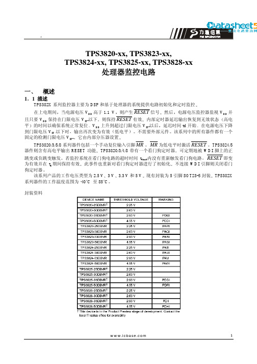
1TPS3820-xx, TPS3823-xx,TPS3824-xx, TPS3825-xx, TPS3828-xx处理器监控电路一 概述1 1 描述TPS382X 系列监控器主要为DSP 和基于处理器的系统提供电路初始化和定时监控在上电期间当电源电压V DD 高于1.1 V 则产生RESET 信号然后电源电压监控器监视V DD 并且只要V DD 保持在门限电压V IT-以下则保持RESET 有效内部定时器延迟输出恢复到无效状态高电平的时间以确保系统正常复位V DD 上升到超过门限电压V IT-以后延迟时间td 开始在电源电压下降到门限电压V IT–以下时输出再次变为有效低电平不需要外部元件该系列中的所有器件都有一个固定的检测门限电压V IT-它由内部分压器设置TPS3820/3/5/8系列器件包括一个手动复位输入引脚MR MR 为低电平时激活RESET TPS3824/5器件则含有高电平输出RESET 功能TPS3820/3/4/8带有一个看门狗定时器可定期地被WDI 脚上的正跳变或负跳变触发若监控系统在看门狗电路的超时时间t t(out)内没有重新触发看门狗电路RESET 即变为有效并在t d 期间保持有效此事件也重新对看门狗定时器进行了初始化不连接WDI 引脚则关闭看门狗定时器该系列产品的工作电压类型为2.5 V 3 V 3.3 V 和5 V 现有封装为5引脚SOT23-5封装TPS382X 系列器件的工作温度范围为–40°C 至85°C封装资料21 2 特点z带有200 ms (TPS3823/4/5/8)或25 ms (TPS3820)固定延迟时间的上电复位发生器z手动复位输入(TPS3820/3/5/8)z推/拉复位(TPS3820/3/4/5)复位(TPS3824)或漏极开路输出(TPS3828)z电源电压监控范围 2.5 V 3 V 3.3 V 和5 V z看门狗定时器(TPS3820/3/4/8)z电源电流为15A 典型值zSOT23-5封装z 温度范围–40°C 至85°C1 3 典型应用z用到DSP 微控制器或微处理器时的应用环境z工业设备z可编程控制z自动化系统z便携式/电池供电设备z智能仪器z无线通信系统z 笔记本/台式计算机典型应用图1 5 功能表1 4 引脚排列图31 6 功能方框图17 时序图二 特性2 1 自然通风工作温度范围内的极限参数*电源电压V DD 见注1 6V 输入电压MR WDI 见注1 –0.3 V 至 (V DD + 0.3V)最低输出电流I OL 5mA 最高输出电流I OH –5mA 输入箝位电流范围I IK (V I < 0或V I > V DD ) ±10mA 输出箝位电流范围I OK (V O < 0或 V O > V DD ) ±10mA4持续总功耗 见额定功耗表自然通风工作温度范围T A –40°C 至85°C 贮存温度范围Tstg –65°C 至150°C 焊接温度 260°C*强度超出所列的极限参数可能导致器件的永久性损坏这些仅仅是极限参数并不意味着在极限条件下或在任何其它超出推荐工作条件所示参数的情况下器件能有效工作延长在极限参数条件下的工作时间会影响器件的可靠性注1所有电压值相对于地额定功耗表22推荐工作条件2 3 在推荐的自然通风工作温度范围内的电特性除非另有规定3为确保门限电压的最佳稳定性应在电源端附近加一个旁路电容器陶瓷0.1F56续前表注4在RESET 被一个P 双向复位引脚激活为低电平时RESET 短路电流为最大上拉电流2 4 定时要求R L = 1 M , C L = 50 pF, T A = 25°C 时2 5 开关特性R L = 1 M , C L = 50 pF, T A = 25°C 时2 6 典型特性78三机械数据注A所有直线尺寸均以毫米为单位B对此图的改变不另行通知C主体部分的尺寸包括模型薄膜或凸出部分声明本资料仅供参考如有不同之处请以相应英文资料为准9。
TPS3823(中文)
1TPS3820-xx, TPS3823-xx,TPS3824-xx, TPS3825-xx, TPS3828-xx处理器监控电路一 概述1 1 描述TPS382X 系列监控器主要为DSP 和基于处理器的系统提供电路初始化和定时监控在上电期间当电源电压V DD 高于1.1 V 则产生RESET 信号然后电源电压监控器监视V DD 并且只要V DD 保持在门限电压V IT-以下则保持RESET 有效内部定时器延迟输出恢复到无效状态高电平的时间以确保系统正常复位V DD 上升到超过门限电压V IT-以后延迟时间td 开始在电源电压下降到门限电压V IT–以下时输出再次变为有效低电平不需要外部元件该系列中的所有器件都有一个固定的检测门限电压V IT-它由内部分压器设置TPS3820/3/5/8系列器件包括一个手动复位输入引脚MR MR 为低电平时激活RESET TPS3824/5器件则含有高电平输出RESET 功能TPS3820/3/4/8带有一个看门狗定时器可定期地被WDI 脚上的正跳变或负跳变触发若监控系统在看门狗电路的超时时间t t(out)内没有重新触发看门狗电路RESET 即变为有效并在t d 期间保持有效此事件也重新对看门狗定时器进行了初始化不连接WDI 引脚则关闭看门狗定时器该系列产品的工作电压类型为2.5 V 3 V 3.3 V 和5 V 现有封装为5引脚SOT23-5封装TPS382X 系列器件的工作温度范围为–40°C 至85°C封装资料21 2 特点z带有200 ms (TPS3823/4/5/8)或25 ms (TPS3820)固定延迟时间的上电复位发生器z手动复位输入(TPS3820/3/5/8)z推/拉复位(TPS3820/3/4/5)复位(TPS3824)或漏极开路输出(TPS3828)z电源电压监控范围 2.5 V 3 V 3.3 V 和5 V z看门狗定时器(TPS3820/3/4/8)z电源电流为15A 典型值zSOT23-5封装z 温度范围–40°C 至85°C1 3 典型应用z用到DSP 微控制器或微处理器时的应用环境z工业设备z可编程控制z自动化系统z便携式/电池供电设备z智能仪器z无线通信系统z 笔记本/台式计算机典型应用图1 5 功能表1 4 引脚排列图31 6 功能方框图17 时序图二 特性2 1 自然通风工作温度范围内的极限参数*电源电压V DD 见注1 6V 输入电压MR WDI 见注1 –0.3 V 至 (V DD + 0.3V)最低输出电流I OL 5mA 最高输出电流I OH –5mA 输入箝位电流范围I IK (V I < 0或V I > V DD ) ±10mA 输出箝位电流范围I OK (V O < 0或 V O > V DD ) ±10mA4持续总功耗 见额定功耗表自然通风工作温度范围T A –40°C 至85°C 贮存温度范围Tstg –65°C 至150°C 焊接温度 260°C*强度超出所列的极限参数可能导致器件的永久性损坏这些仅仅是极限参数并不意味着在极限条件下或在任何其它超出推荐工作条件所示参数的情况下器件能有效工作延长在极限参数条件下的工作时间会影响器件的可靠性注1所有电压值相对于地额定功耗表22推荐工作条件2 3 在推荐的自然通风工作温度范围内的电特性除非另有规定3为确保门限电压的最佳稳定性应在电源端附近加一个旁路电容器陶瓷0.1F56续前表注4在RESET 被一个P 双向复位引脚激活为低电平时RESET 短路电流为最大上拉电流2 4 定时要求R L = 1 M , C L = 50 pF, T A = 25°C 时2 5 开关特性R L = 1 M , C L = 50 pF, T A = 25°C 时2 6 典型特性78三机械数据注A所有直线尺寸均以毫米为单位B对此图的改变不另行通知C主体部分的尺寸包括模型薄膜或凸出部分声明本资料仅供参考如有不同之处请以相应英文资料为准9。
HSMP-3892中文资料

Surface Mount PIN Diodes Technical DataFeatures•Diodes Optimized for:Low Current SwitchingLow Distortion AttenuatingUltra-Low DistortionSwitchingMicrowave FrequencyOperation•Surface Mount SOT-23 and SOT-143 PackagesSingle and Dual VersionsTape and Reel OptionsAvailable•Low Failure in Time (FIT) Rate[1]Note:1.For more information see theSurface Mount PIN Reliability Data Sheet.HSMP-38XX andHSMP-48XX SeriesPackage Lead CodeIdentificationrequired. The HSMP-48XX seriesare special products featuringultra low parasitic inductance inthe SOT-23 package, specificallydesigned for use at frequencieswhich are much higher than theupper limit for conventionalSOT-23 PIN diodes. TheHSMP-4810 diode is a low distor-tion attenuating PIN designed foroperation to 3 GHz. TheHSMP-4820 diode is ideal forlimiting and low inductanceswitching applications up to1.5GHz. The HSMP-4890 isoptimized for low current switch-ing applications up to 3 GHz.The HSMP-386X series of generalpurpose PIN diodes are designedfor two classes of applications.The first is attenuators wherecurrent consumption is the mostimportant design consideration.The second application for thisseries of diodes is in switcheswhere low cost is the drivingissue for the designer.The HSMP-386X series TotalCapacitance (C T) and TotalResistance (R T) are typicalspecifications. For applicationsthat require guaranteed perfor-mance, the general purposeHSMP-383X series is recom-Description/Applications The HSMP-380X and HSMP-381X series are specifically designed for low distortion attenuator applica-tions. The HSMP-382X series is optimized for switching applica-tions where ultra-low resistance is required. The HSMP-3880 switch-ing diode is an ultra low distortion device optimized for higher power applications from 50 MHz to1.5GHz. The HSMP-389X series is optimized for switching applica-tions where low resistance at low attenuators, the HSMP-380X or -381X series are recommended. For high performance switching applications, the HSMP-389X series is recommended.A SPICE model is not available for PIN diodes as SPICE does not provide for a key PIN diode characteristic, carrier lifetime.Absolute Maximum Ratings [1] T A = 25°CSymbol ParameterUnits Absolute Maximum I f Forward Current (1 ms Pulse)Amp 1P t Total Device Dissipation mW [2]250P iv Peak Inverse Voltage —Same as V BRT j Junction Temperature °C 150T STGStorage Temperature°C-65 to 150Notes:1.Operation in excess of any one of these conditions may result in permanent damage to this device.2.CW Power Dissipation at T LEAD = 25°C. Derate to zero at maximum rated temperature.PIN Switching DiodesElectrical Specifications T A = 25°CNearest Maximum Equivalent Minimum Maximum Maximum Shunt Mode Part Package Axial Lead Breakdown Series Total Harmonic Number Marking LeadPart No.Voltage Resistance Capacitance Distortion HSMP-Code [1]Code Configuration 5082-V BR (V)R S (Ω)C T (pF)Hmd (dBc)3820F00Single 3188500.6*0.8*—3822F22Series3823F33Common Anode 3824F44Common Cathode 3880S00Single—100 6.50.40–553890G00Single —1002.50.30**—3892G22Series3893G33Common Anode 3894G44Common Cathode 3895G55Unconnected PairTest ConditionsV R = V BR I F = 5 mA V R = 50 V 2 f o, Z o = 50 W Measure f = 100 MHz f = 1 MHz f o = 400 MHz I R ≤ 10 µA I F = 10 mA*V R = 20 V*P in = +30 dBm V R = 5 V**0 V biasPIN Attenuator DiodesElectrical Specifications T A = 25°C (Each Diode)NearestEquivalent Minimum Maximum Maximum Minimum Maximum Part Package Axial Lead Breakdown Series Total High Low Number Marking LeadPart No.Voltage Resistance Capacitance Resistance Resistance HSMP-Code [1]Code Configuration 5082-V BR (V)R S (Ω)C T (pF)R H (Ω)R L (Ω)3800D00Single 30801002.00.37100083802D22Series3804D44Common Cathode 3810E00Single 3081100 3.00.351500103812E22Series3813E33Common Anode 3814E44Common CathodeTest ConditionsV R = V BR I F = 100 mA V R = 50 V I F = 0.01 mA I F = 20 mA Measure f = 100 MHz f = 1 MHz f = 100 MHz f= 100 MHzI R ≤ 10 µAPIN General Purpose Diodes, Electrical Specifications T A = 25°CNearestEquivalent Minimum Maximum Maximum Part Package Axial Lead Breakdown Series Total Number Marking Lead Part No.Voltage Resistance Capacitance HSMP-Code[1]Code Configuration5082-V BR (V)R S (Ω)C T (pF) 3830K00Single3077200 1.50.3 3832K22Series3833K33Common Anode3834K44Common CathodeTest Conditions V R = V BR I F = 100 mA V R = 50 VMeasure f = 100 MHz f = 1 MHzI R≤ 10 mAHigh Frequency (Low Inductance, 500 MHz – 3 GHz) PIN Diodes, Electrical Specifications T A = 25°CMinimum Maximum Typical Maximum TypicalBreak-Series Total Total Total Part Package down Resis-Capaci-Capaci-Induc-Number Marking Lead Config-Voltage tance tance tance tance Appli-HSMP-Code Code uration V BR (V)R S (Ω)C T (pF)C T (pF)L T (nH)cation 4810EB B Dual100 3.00.350.4 1.0Attenu-Cathode ator 4820FA A Dual Anode500.6*0.75* 1.0 1.0*Limiter 4890GA A Dual Anode100 2.5**0.330.375 1.0SwitchV R = V BR I F = 100 mA V R = 50 V V R = 50 V f = 500 MHz –Measure I F = 10 mA* f = 1 MHz f = 1 MHz 3 GHzI R≤ 10 µA I F = 5 mA**V R = 20 V*V R = 0 V V R = 20 V*PIN General Purpose Diodes, Typical Specifications T A = 25°CCode Minimum Typical Series Typical Total Part Number Marking Lead Breakdown Resistance Capacitance HSMP-Code[1]Code Configuration Voltage V BR (V)R S (Ω)C T (pF)3860L00Single50 3.0/1.5*0.203862L22Series3863L33Common Anode3864L44Common CathodeTest Conditions V R = V BR I F = 10 mA V R = 50 VMeasure f = 100 MHz f = 1 MHzI R≤ 10 µA*I F = 100 mATypical Parameters at T A = 25°CPart Number Series Resistance Carrier Lifetime Reverse Recovery Time Total Capacitance HSMP-R S (Ω)τ (ns)T rr (ns)C T (pF)380X5518005000.32 @ 50 V381X7515003000.27 @ 50 V382X 1.570*70.60 @ 20 V383X20500800.20 @ 50 V388X 3.825005500.30 @ 50 V389X 3.8200*–0.20 @ 5 V Test Conditions I F = 1 mA I F = 50 mA V R = 10 Vf = 100 MHz I R = 250 mA I F = 20 mAI F = 10 mA*I F = 10 mA*90% RecoveryI R = 6 mA*Typical Parameters at T A = 25°C (unless otherwise noted), Single DiodeFigure 2. RF Capacitance vs. Reverse Bias, HSMP-3830 Series.0.150.300.250.200.350.400.45T O T A L C A P A C I T A N C E (p F )REVERSE VOLTAGE (V)Figure 1. RF Capacitance vs. Reverse Bias, HSMP-3810 Series.Figure 3. Resistance at 25°C vs. Forward Bias Current.0.150.300.250.200.35T O T A L C A P A C I T A N C E (p F )REVERSE VOLTAGE (V)R E S I S T A N C E (O H M S )I F – FORWARD BIAS CURRENT (mA)0.010.11101000.010.1110100R F R E S I S T A N C E (O H M S )I F – FORWARD BIAS CURRENT (mA)R F R E S I S T A N C E (O H M S )0.010.1110100I F – FORWARD BIAS CURRENT (mA)Figure 5. RF Resistance vs. Forward Bias Current for HSMP-3810/HSMP-4810.V R – REVERSE VOLTAGE (V)C A P A C I T A N C E (p F )Figure 6. Capacitance vs. Reverse Voltage.Figure 4. RF Resistance vs. Forward Bias Current for HSMP-3800.100010010DIODE RF RESISTANCE (OHMS)Figure 7. 2nd Harmonic Input Intercept Point vs. Diode RFResistance for Attenuator Diodes.I N P U T I N T E R C E P T P O I N T (d B m )12011511010510095908511030I F – FORWARD BIAS CURRENT (mA)Figure 8. 2nd Harmonic Input Intercept Point vs. Forward Bias Current for Switch Diodes.I N P U T I N T E R C E P T P O I N T (d B m )FORWARD CURRENT (mA)Figure 9. Reverse Recovery Time vs. Forward Current for Various Reverse Voltages. HSMP-3820 Series.T r r – R E V E R S E R E C O V E R Y T I M E (n s )110100102030V R = 2V V R = 5VV R = 10VHSMP-382XTypical Parameters (continued)100010010102030T r r - R E V E R S E R E C O V E R Y T I M E (n S )FORWARD CURRENT (mA)Figure 10. Reverse Recovery Time vs. Forward Current for Various Reverse Voltage. HSMP-3830 Series.HSMP-3830V R = 5VV R = 10V V R = 20VR E V E R S E R E C O V E R Y T I M E (n S )FORWARD CURRENT (mA)Figure 11. Typical Reverse Recovery Time vs. Reverse Voltage. HSMP-3880 Series.1020152530T R R - R E V E R S E R E C O V E R Y T I M E (n S )FORWARD CURRENT (mA)Figure 12. Typical Reverse Recovery Time vs. Reverse Voltage. HSMP-3890 Series.1001010.10.01I F – F O R W A R D C U R R E N T (m A )I F – F O R W A R D C U R R E N T (m A )V F – FORWARD VOLTAGE (mA)Figure 14. Forward Current vs. Forward Voltage. HSMP-3810 and HSMP-4810 Series.V F – FORWARD VOLTAGE (mA)Figure 15. Forward Current vs. Forward Voltage. HSMP-3820 and HSMP-4820 Series.1001010.10.01I F – F O R W A R D C U R R E N T (m A )V F – FORWARD VOLTAGE (mA)Figure 16. Forward Current vs.Forward Voltage. HSMP-3830 Series.00.20.40.60.81.01.2I F – F O R W A R D C U R R E N T (m A )V F – FORWARD CURRENT (mA)Figure 17. Forward Current vs.Forward Voltage. HSMP-3880 Series.0.20.40.60.81.01.2V F – FORWARD VOLTAGE (mA)Figure 18. Forward Current vs. Forward Voltage. HSMP-3890 and HSMP-4890 Series.Typical Parameters (continued)Figure 19. Typical RF Resistance vs. Forward Bias Current for HSMP-3860.Figure 20. Forward Current vs. Forward Voltage for HSMP-3860.Figure 21. Typical Capacitance vs. Reverse Bias for HSMP-3860.10001R E S I S T A N C E (O HM S )BIAS CURRENT (mA)10100I F – F O R W A R D C U R R E N T (m A )V F – FORWARD VOLTAGE (V)0200.515C T – C A P A C I T A N C E (p F )V R – REVERSE VOLTAGE (V)0.20.41050.10.30.12 pF** Measured at -20 V C p 0.08 pFR j = 12ΩI 0.9C T = C P + C jI = Forward Bias Current in mAEquivalent Circuit ModelHSMS-3860Typical Applications for Multiple Diode ProductsRF COMMONRF 1RF 1Figure 24. Switch Using Both Positive and Negative Bias Current.Figure 25. Very High Isolation SPDT Switch, Dual Bias.Typical Applications for Multiple Diode Products (continued)INPUT RF IN/OUTFigure 26. Four Diode π Attenuator.Figure 27. High Isolation SPST Switch (Repeat Cells as Required).VOLTAGEBIASFigure 28. Power Limiter Using HSMP-3822Diode Pair.Typical Applications for HSMP-48XX Low Inductance SeriesFigure 29. Internal Connections.HSMP-4820 & HSMP-4890HSMP-48100.5 nH*0.8pF TYPICAL FOR HSMP-3820Figure 30. Equivalent Circuit.*0.8 pF TYPICAL FOR HSMP-3820Figure 32. Equivalent Circuit.Figure 31. Circuit Layout.Microstrip SeriesConnection for HSMP-48XX SeriesIn order to take full advantage of the low inductance of the HSMP-48XX series when using them in series application,both lead 1 and lead 2 should beconnected together, as shown above.Microstrip Shunt Connections for HSMP-48XX SeriesIn the diagram above, the center conductor of themicrostrip line is interrupted and leads 1 and 2 of theHSMP-38XX series diode are placed across the resulting gap. This forces the 0.5 nH lead inductance of leads 1 and 2 to appear as part of a low pass filter, reducing the shunt parasitic inductance andincreasing the maximumavailable attenuation. The 0.3 nH of shunt inductance external to the diode is created by the via holes, and is a good estimate for 0.032" thick material.Co-Planar Waveguide Shunt Connection for HSMP-48XX SeriesCo-Planar waveguide, with ground on the top side of the printed circuit board, is shownin the diagram above. Since it eliminates the need for via holes to ground, it offers lower shunt parasitic inductance and higher maximum attenuation whencompared to a microstrip circuit.GROUND BY TWOVIA HOLES*0.8 pF TYPICAL FOR HSMP-4820Figure 34. Equivalent Circuit.Figure 33. Circuit Layout.*0.8 pF TYPICAL FOR HSMP-4820Figure 36. Equivalent Circuit.Figure 35. Circuit Layout.11Package DimensionsOutline 23 (SOT-23)PC Board FootprintsSOT-23Package CharacteristicsLead Material......................................................................................Alloy 42Lead Finish............................................................................Tin-Lead 85-15%Maximum Soldering Temperature..............................260°C for 5 seconds Minimum Lead Strength..........................................................2 pounds pull Typical Package Inductance ..................................................................2 nH Typical Package Capacitance ..............................0.08 pF (opposite leads)SOT-143Outline 143 (SOT-143)SIDE VIEWEND VIEWDIMENSIONS ARE IN MILLIMETERS (INCHES)DIMENSIONS ARE IN MILLIMETERS (INCHES)PACKAGE MARKING/go/rfFor technical assistance or the location of your nearest Hewlett-Packard salesoffice, distributor or representative call:Americas/Canada: 1-800-235-0312 or 408-654-8675Far East/Australasia: Call your local HP sales office.Japan: (81 3) 3335-8152Europe: Call your local HP sales office.Data subject to change.Copyright © 1999 Hewlett-Packard Co.Obsoletes 5968-3435E5968-5439E (6/99)Profile Option Descriptions-BLK = Bulk-TR1 = 3K pc. Tape and Reel, Device Orientation; See Figures 37 and 38-TR2 = 10K pc. Tape and Reel, Device Orientation; See Figures 37 and 38Tape and Reeling conforms to Electronic Industries RS-481, “Taping of Surface Mounted Components for Automated Placement.”Ordering InformationSpecify part number followed by option under. For example:H SMP -38XX -XXXBulk or Tape and Reel OptionPart NumberSurface Mount PIN Diode Hewlett-PackardUSER FEEDEND VIEWTOP VIEW Figure 37. Options -TR1, -TR2 for SOT-23 Packages.Figure 38. Options -TR1, -TR2 for SOT-143 Packages.END VIEWTOP VIEW。
TSOP38238中文资料

IR Receiver Modules for Remote Control SystemsTSOP382.., TSOP384.. Vishay SemiconductorsMECHANICAL DATA Pinning:1 = OUT,2 = GND,3 = V S FEATURES•Very low supply current•Photo detector and preamplifier in one package •Internal filter for PCM frequency•Improved shielding against EMI•Supply voltage: 2.5 V to 5.5 V•Improved immunity against ambient light•Insensitive to supply voltage ripple and noise •Component in accordance to RoH S 2002/95/EC and WEEE 2002/96/ECDESCRIPTIONThe TSOP382.., TSOP384.. series are miniaturized receivers for infrared remote control systems. A PIN diode and a preamplifier are assembled on a lead frame, the epoxy package acts as an IR filter.The demodulated output signal can be directly decoded by a microprocessor. The TSOP382.. is compatible with all common IR remote control data formats. The TSOP384.. is optimized to suppress almost all spurious pulses from energy saving fluorescent lamps but will also suppress some data signals.This component has not been qualified according to automotive specifications.BLOCK DIAGRAM APPLICATION CIRCUIT19026PARTS TABLECARRIER FREQUENCY STANDARD APPLICATIONS (AGC2/AGC8)VERY NOISY ENVIRONMENTS (AGC4) 30 kHz TSOP38230TSOP3843033 kHz TSOP38233TSOP3843336 kHz TSOP38236TSOP3843638 kHz TSOP38238TSOP3843840 kHz TSOP38240TSOP3844056 kHz TSOP38256TSOP38456TSOP382.., TSOP384..IR Receiver Modules for Remote Control SystemsVishay SemiconductorsNote(1)Stresses beyond those listed under “Absolute Maximum Ratings” may cause permanent damage to the device. This is a stress rating only and functional operation of the device at these or any other conditions beyond those indicated in the operational sections of this specification is not implied. Exposure to absolute maximum rating condtions for extended periods may affect the device reliability.Note (1)T amb = 25°C, unless otherwise specifiedTYPICAL CHARACTERISTICST amb = 25°C, unless otherwise specifiedFig. 1 - Output Active LowFig. 2 - Pulse Length and Sensitivity in Dark AmbientABSOLUTE MAXIMUM RATINGS (1)PARAMETER TEST CONDITIONSYMBOLVALUE UNIT Supply voltage (pin 3)V S - 0.3 to + 6.0V Supply current (pin 3)I S 3mA Output voltage (pin 1)V O - 0.3 to (V S + 0.3)V Output current (pin 1)I O 5mA Junction temperatureT j 100°C Storage temperature range T stg - 25 to + 85°C Operating temperature range T amb - 25 to + 85°C Power consumption T amb ≤ 85°C P tot 10mW Soldering temperaturet ≤ 10 s, 1 mm from case T sd260°CELECTRICAL AND OPTICAL CHARACTERISTICS (1)PARAMETER TEST CONDITION SYMBOL MIN.TYP.MAX.UNIT Supply current (pin 3)E v = 0, V S = 3.3 V I SD 0.270.350.45mA E v = 40 klx, sunlightI SH 0.45mA Supply voltage V S 2.55.5V Transmission distance E v = 0, test signal see fig. 1,IR diode TSAL6200,I F = 250 mA d 45m Output voltage low (pin 1)I OSL = 0.5 mA, E e = 0.7 mW/m 2,test signal see fig. 1V OSL 100mV Minimum irradiance Pulse width tolerance:t pi - 5/f o < t po < t pi + 6/f o ,test signal see fig. 1E e min.0.150.35mW/m 2Maximum irradiance t pi - 5/f o < t po < t pi + 6/f o ,test signal see fig. 1E e max.30W/m 2DirectivityAngle of half transmission distanceϕ1/2± 45degE eV O V VTSOP382.., TSOP384..Vishay SemiconductorsIR Receiver Modules for Remote Control SystemsFig. 3 - Output FunctionFig. 4 - Output Pulse DiagramFig. 5 - Frequency Dependence of ResponsivityFig. 6 - Sensitivity in Bright AmbientFig. 7 - Sensitivity vs. Supply Voltage DisturbancesFig. 8 - Sensitivity vs. Electric Field DisturbancesE eV O V V OL0.00.20.40.60.81.01.20.70.9 1.1 1.3f/f 0 - Relati v e Fre qu ency16925E /E - R e l. R e s p o n s i v i t y e m i n.eTSOP382.., TSOP384.. IR Receiver Modules forRemote Control SystemsVishay SemiconductorsFig. 9 - Max. Envelope Duty Cycle vs. Burst Length Fig. 10 - Sensitivity vs. Ambient Temperature Fig. 11 - Relative Spectral Sensitivity vs. WavelengthFig. 12 - Horizontal DirectivityFig. 13 - Vertical Directivity Fig. 14 - Sensitivity vs. Supply VoltageTSOP382.., TSOP384..Vishay SemiconductorsIR Receiver Modules for Remote Control SystemsSUITABLE DATA FORMATThe TSOP382.., TSOP384.. series are designed to suppress spurious output pulses due to noise or disturbance signals.Data and disturbance signals can be distinguished by the devices according to carrier frequency, burst length and envelope duty cycle. The data signal should be close to the band-pass center frequency (e.g. 38 kH z) and fulfill the conditions in the table below.When a data signal is applied to the TSOP382.., TSOP384..in the presence of a disturbance signal, the sensitivity of the receiver is reduced to insure that no spurious pulses are present at the output. Some examples of disturbance signals which are suppressed are:•DC light (e.g. from tungsten bulb or sunlight)•Continuous signals at any frequency•Strongly or weakly modulated noise from fluorescent lamps with electronic ballasts (see figure 15 or figure 16)Fig. 15 - IR Signal from Fluorescent Lampwith Low ModulationFig. 16 - IR Signal from Fluorescent Lampwith High ModulationNoteFor data formats with short bursts please see the datasheet for TSOP381.., TSOP383..0101520Time (ms)16920I R S i g n a l50101520Time (ms)16921I R S i g n a l10TSOP382..TSOP384..Minimum burst length10 cycles/burst 10 cycles/burst After each burst of lengtha minimum gap time is required of10 to 70 cycles ≥ 10 cycles 10 to 35 cycles ≥ 10 cycles For bursts greater thana minimum gap time in the data stream is needed of 70 cycles > 4 x burst length35 cycles> 10 x burst lengthMaximum number of continuous short bursts/second 18001500Compatible to NEC code yes yes Compatible to RC5/RC6 code yes yes Compatible to Sony codeyes no Compatible to Thomson 56 kHz codeyes yes Compatible to Mitsubishi code (38 kHz, preburst 8 ms, 16 bit)yes no Compatible to Sharp codeyesyesSuppression of interference from fluorescent lampsMost common disturbance signals are suppressedEven extreme disturbance signals are suppressedTSOP382.., TSOP384..IR Receiver Modules forVishay SemiconductorsRemote Control SystemsPACKAGE DIMENSIONS in millimetersTSOP382.., TSOP384..Vishay Semiconductors IR Receiver Modules forRemote Control SystemsOZONE DEPLETING SUBSTANCES POLICY STATEMENTIt is the policy of Vishay Semiconductor GmbH to1.Meet all present and future national and international statutory requirements.2.Regularly and continuously improve the performance of our products, processes, distribution and operating systems withrespect to their impact on the health and safety of our employees and the public, as well as their impact on the environment. It is particular concern to control or eliminate releases of those substances into the atmosphere which are known as ozone depleting substances (ODSs).The Montreal Protocol (1987) and its London Amendments (1990) intend to severely restrict the use of ODSs and forbid their use within the next ten years. Various national and international initiatives are pressing for an earlier ban on these substances. Vishay Semiconductor GmbH has been able to use its policy of continuous improvements to eliminate the use of ODSs listed in the following documents.1.Annex A, B and list of transitional substances of the Montreal Protocol and the London Amendments respectively.2.Class I and II ozone depleting substances in the Clean Air Act Amendments of 1990 by the Environmental Protection Agency(EPA) in the USA.3.Council Decision 88/540/EEC and 91/690/EEC Annex A, B and C (transitional substances) respectively.Vishay Semiconductor GmbH can certify that our semiconductors are not manufactured with ozone depleting substances and do not contain such substances.We reserve the right to make changes to improve technical designand may do so without further notice.Parameters can vary in different applications. All operating parameters must be validated for each customer application by the customer. Should the buyer use Vishay Semiconductors products for any unintended or unauthorized application, the buyer shall indemnify Vishay Semiconductors against all claims, costs, damages, and expenses, arising out of, directly or indirectly, any claim of personal damage, injury or death associated with such unintended or unauthorized use.Vishay Semiconductor GmbH, P.O.B. 3535, D-74025 Heilbronn, GermanyDisclaimer Legal Disclaimer NoticeVishayAll product specifications and data are subject to change without notice.Vishay Intertechnology, Inc., its affiliates, agents, and employees, and all persons acting on its or their behalf (collectively, “Vishay”), disclaim any and all liability for any errors, inaccuracies or incompleteness contained herein or in any other disclosure relating to any product.Vishay disclaims any and all liability arising out of the use or application of any product described herein or of any information provided herein to the maximum extent permitted by law. The product specifications do not expand or otherwise modify Vishay’s terms and conditions of purchase, including but not limited to the warranty expressed therein, which apply to these products.No license, express or implied, by estoppel or otherwise, to any intellectual property rights is granted by this document or by any conduct of Vishay.The products shown herein are not designed for use in medical, life-saving, or life-sustaining applications unless otherwise expressly indicated. Customers using or selling Vishay products not expressly indicated for use in such applications do so entirely at their own risk and agree to fully indemnify Vishay for any damages arising or resulting from such use or sale. Please contact authorized Vishay personnel to obtain written terms and conditions regarding products designed for such applications.Product names and markings noted herein may be trademarks of their respective owners.元器件交易网。
HSMP-389V-BLK中文资料

Surface Mount RF PIN Switch DiodesTechnical DataFeatures•Unique Configurations in Surface Mount Packages–Add Flexibility–Save Board Space–Reduce Cost•Switching–Low Capacitance–Low Resistance at LowCurrent•Low Failure in Time (FIT) Rate[1]•Matched Diodes forConsistent Performance •Better ThermalConductivity for HigherPower Dissipation•Lead-free Option Available Note:1.For more information see theSurface Mount PIN Reliability Data Sheet.HSMP-389x SeriesHSMP-489x SeriesDescription/ApplicationsThe HSMP-389x series isoptimized for switching applica-tions where low resistance at lowcurrent and low capacitance arerequired. The HSMP-489x seriesproducts feature ultra lowparasitic inductance. Theseproducts are specificallydesigned for use at frequencieswhich are much higher than theupper limit for conventional PINdiodes.654Notes:1.Package marking providesorientation, identification, anddate code.2.See “Electrical Specifications” forappropriate package marking.Pin Connections andPackage Marking2Package Lead CodeIdentification, SOT-23/143(Top View)Package Lead CodeIdentification, SOT-323(Top View)Package Lead CodeIdentification, SOT-363(Top View)Absolute Maximum Ratings [1] T C = +25°CSymbol ParameterUnit SOT-23/143SOT-323/363I f Forward Current (1 µs Pulse)Amp 11P IV Peak Inverse Voltage V 100100T j Junction Temperature °C 150150T stg Storage Temperature °C -65 to 150-65 to 150θjcThermal Resistance [2]°C/W500150Notes:1.Operation in excess of any one of these conditions may result in permanent damage to the device.2.T C = +25°C, where T C is defined to be the temperature at the package pins where contact is made to the circuit board.ESD WARNING:Handling Precautions Should Be Taken To Avoid Static Discharge.UNCONNECTEDTRIOVDUAL SWITCHMODEL3Electrical Specifications, TC= 25°C, each diodePackage Minimum Maximum Maximum Part Number Marking Lead Breakdown Series Resistance Total Capacitance HSMP-Code Code Configuration Voltage V BR (V)R S (Ω)C T (pF) 3890G0[1]0Single100 2.50.303892G2[1]2Series3893G3[1]3Common Anode3894G4[1]4Common Cathode3895G5[1]5Unconnected Pair389B G0[2]B Single389C G2[2]C Series389E G3[2]E Common Anode389F G4[2]F Common Cathode389L GL[2]L Unconnected Trio389R S[2]R Dual Switch Mode389T Z[2]T Low Inductance Single389U GU[2]U Series-Shunt Pair389V GV[2]V High Frequency Series PairTest Conditions V R = V BR I F = 5 mA V R = 5 VMeasure f = 100 MHz f = 1 MHzI R≤ 10 µANotes:1.Package marking code is white.2.Package is laser marked.High Frequency (Low Inductance, 500MHz–3GHz) PIN DiodesMinimum Maximum Typical Maximum Typical Part Package Breakdown Series Total Total Total Number Marking Voltage Resistance Capacitance Capacitance Inductance HSMP-Code[1]Configuration V BR (V)R S (Ω)C T (pF)C T (pF)L T (nH) 489x GA Dual Anode100 2.50.330.375 1.0 Test Conditions V R = V BR I F = 5 mA f = 1 MHz V R = 5 V f=500 MHz– Measure V R = 5V f = 1 MHz 3 GHzIR≤ 10 µANote:1.SOT-23 package marking code is white; SOT-323 is laser marked.Typical Parameters at T C = 25°CPart Number Series Resistance Carrier Lifetime Total CapacitanceHSMP-RS (Ω)τ (ns)CT(pF)389x 3.82000.20 @ 5V Test Conditions I F = 1 mA I F = 10 mAf = 100 MHz I R = 6 mA4HSMP-389x Series Typical Performance, T C = 25°C, each diodeTypical Applications for Multiple Diode Products1001010.1R F R E S I S T A N C E (O H M S )11030I F – FORWARD BIAS CURRENT (mA)Figure 3. 2nd Harmonic Input Intercept Point vs. Forward Bias Current.I N P U T I N T E R C E P T P O I N T (d B m )T r r – R E V E R S E R E C O V E R Y T I M E (n S )FORWARD CURRENT (mA)Figure 4. Typical Reverse Recovery Time vs. Reverse Voltage.00.20.40.60.81.01.2V F – FORWARD VOLTAGE (V)Figure 5. Forward Current vs. Forward Voltage.3RF inFigure 6. HSMP-389L used in a SP3T Switch.Figure 7. HSMP-389L Unconnected Trio used in a Dual Voltage, High Isolation Switch.5Typical Applications for Multiple Diode Products (continued)Figure 11. HSMP-389V Series/Shunt Pair used in a 1.8GHz Transmit/Receive Switch.Figure 10. HSMP-389U Series/Shunt Pair used in a 900MHz Transmit/Receive Switch.Figure 8. HSMP-389L Unconnected Trio used in a Positive Voltage, High Isolation Switch.Figure 9. HSMP-389T used in a Low Inductance Shunt Mounted Switch.RcvrXmtrRcvr6Typical Applications for Multiple Diode Products (continued)RF COMMONRF 1RF 1Figure 14. Switch Using Both Positive and Negative Bias Current.Figure 15. Very High Isolation SPDT Switch, Dual Bias.7Equivalent Circuit ModelHSMP-389x Chip*0.12 pF** Measured at -20 VR j = 20 ΩI 0.9R T = 0.5 + R j C T = C P + C jI = Forward Bias Current in mA * See AN1124 for package modelsTypical Applications for HSMP-489x Low Inductance SeriesMicrostrip Series Connection for HSMP-489x SeriesIn order to take full advantage of the low inductance of the HSMP-489x series when using them in series applications, both lead 1 and lead 2 should beconnected together, as shown inFigure 17.HSMP-489xFigure 16. Internal Connections.Figure 17. Circuit Layout.Microstrip Shunt Connections for HSMP-489x SeriesIn Figure 18, the center conductor of the microstrip line is inter-rupted and leads 1 and 2 of the HSMP-489x diode are placed across the resulting gap. This forces the 1.5 nH lead inductance of leads 1 and 2 to appear as part of a low pass filter, reducing the shunt parasitic inductance and increasing the maximum available attenuation. The 0.3nH of shunt inductance external to the diode is created by the via holes, and is a good estimate for 0.032" thick material.GROUND BY TWOVIA HOLESFigure 18. Circuit Layout.Figure 19. Equivalent Circuit.Co-Planar Waveguide Shunt Connection for HSMP-489x SeriesCo-Planar waveguide, with ground on the top side of theprinted circuit board, is shown in Figure 20. Since it eliminates the need for via holes to ground, it offers lower shunt parasiticinductance and higher maximum attenuation when compared to a microstrip circuit.Figure 20. Circuit Layout.Figure 21. Equivalent Circuit.A SPICE model is not available for PIN diodes as SPICE does not provide for a key PIN diode characteristic, carrier lifetime.8Assembly InformationFigure 22. PCB Pad Layout, SOT-363.(dimensions in inches).Figure 23. PCB Pad Layout, SOT-323.(dimensions in inches).Figure 24. PCB Pad Layout, SOT-23.Figure 25. PCB Pad Layout, SOT-143.TIME (seconds)T E M P E R A T U R E (°C )05010015020025060120180240300Figure 26. Surface Mount Assembly Profile.SMT AssemblyReliable assembly of surface mount components is a complex process that involves manymaterial, process, and equipment factors, including: method of heating (e.g., IR or vapor phase reflow, wave soldering, etc.)circuit board material, conductor thickness and pattern, type of solder alloy, and the thermalconductivity and thermal mass of components. Components with a low mass, such as the SOTpackage, will reach solder reflow temperatures faster than those with a greater mass.Agilent ’s diodes have beenqualified to the time-temperature profile shown in Figure 26. This profile is representative of an IR reflow type of surface mount assembly process.After ramping up from room temperature, the circuit board with components attached to it (held in place with solder paste)passes through one or morepreheat zones. The preheat zones increase the temperature of the board and components to prevent thermal shock and begin evaporat-ing solvents from the solder paste.The reflow zone briefly elevates the temperature sufficiently to produce a reflow of the solder.The rates of change of tempera-ture for the ramp-up and cool-down zones are chosen to be low enough to not cause deformation of the board or damage to compo-nents due to thermal shock. The maximum temperature in the reflow zone (T MAX ) should not exceed 235°C.These parameters are typical for a surface mount assembly process for Agilent diodes. As a general guideline, the circuit board and components should be exposed only to the minimum tempera-tures and times necessary to achieve a uniform reflow of solder.9Package CharacteristicsLead Material....................Copper (SOT-323/363); Alloy 42 (SOT-23/143)Lead Finish............................................................................Tin-Lead 85-15%Maximum Soldering Temperature..............................260°C for 5 seconds Minimum Lead Strength..........................................................2 pounds pull Typical Package Inductance ..................................................................2 nH Typical Package Capacitance ..............................0.08 pF (opposite leads)Package DimensionsOutline 23 (SOT-23)Outline 143 (SOT-143)SIDE VIEWEND VIEWDIMENSIONS ARE IN MILLIMETERS (INCHES)DIMENSIONS ARE IN MILLIMETERS (INCHES)PACKAGE MARKING CODE (XX)Outline SOT-363 (SC-70 6 Lead)Outline SOT-323 (SC-70 3 Lead)0.25 (0.010)0.15 (0.006)0.30 (0.012)0.10 (0.004)0.425 (0.017)DIMENSIONS ARE IN MILLIMETERS (INCHES)0.30 (0.012)0.10 (0.004)0.425 (0.017)DIMENSIONS ARE IN MILLIMETERS (INCHES)10Ordering InformationSpecify part number followed by option. For example:HSMP -389x -XXXBulk or Tape and Reel Option Part Number; x = Lead Code Surface Mount PINOption Descriptions-BLK = Bulk, 100 pcs. per antistatic bag-TR1 = Tape and Reel, 3000 devices per 7" reel -TR2 = Tape and Reel, 10,000 devices per 13" reelTape and Reeling conforms to Electronic Industries RS-481, “Taping of Surface Mounted Components for Automated Placement.”For lead-free option, the part number will have the character "G" at the end, eg. -TR2G for a 10K pc lead-free reel.Device OrientationUSER FEEDFor Outline SOT-143Note: "AB" represents package marking code. "C" represents date code.END VIEWTOP VIEW For Outlines SOT-23, -323Note: "AB" represents package marking code. "C" represents date code.END VIEWTOP VIEW END VIEWTOP VIEW Note: "AB" represents package marking code. "C" represents date code.For Outline SOT-36311Tape Dimensions and Product OrientationFor Outline SOT-23DESCRIPTIONSYMBOL SIZE (mm)SIZE (INCHES)LENGTH WIDTH DEPTH PITCHBOTTOM HOLE DIAMETER A 0B 0K 0P D 1 3.15 ± 0.102.77 ± 0.101.22 ± 0.104.00 ± 0.101.00 + 0.050.124 ± 0.0040.109 ± 0.0040.048 ± 0.0040.157 ± 0.0040.039 ± 0.002CAVITYDIAMETER PITCH POSITION D P 0E 1.50 + 0.104.00 ± 0.101.75 ± 0.100.059 + 0.0040.157 ± 0.0040.069 ± 0.004PERFORATIONWIDTH THICKNESSW t18.00 + 0.30 – 0.100.229 ± 0.0130.315 + 0.012 – 0.0040.009 ± 0.0005CARRIER TAPE CAVITY TO PERFORATION (WIDTH DIRECTION)CAVITY TO PERFORATION (LENGTH DIRECTION)F P 23.50 ± 0.052.00 ± 0.050.138 ± 0.0020.079 ± 0.002DISTANCE BETWEEN CENTERLINE1DESCRIPTIONSYMBOL SIZE (mm)SIZE (INCHES)LENGTH WIDTH DEPTH PITCHBOTTOM HOLE DIAMETER A 0B 0K 0P D 1 3.19 ± 0.102.80 ± 0.101.31 ± 0.104.00 ± 0.101.00 + 0.250.126 ± 0.0040.110 ± 0.0040.052 ± 0.0040.157 ± 0.0040.039 + 0.010CAVITYDIAMETER PITCH POSITION D P 0E 1.50 + 0.104.00 ± 0.101.75 ± 0.100.059 + 0.0040.157 ± 0.0040.069 ± 0.004PERFORATIONWIDTH THICKNESSW t18.00 + 0.30 – 0.100.254 ± 0.0130.315+ 0.012 – 0.0040.0100 ± 0.0005CARRIER TAPE CAVITY TO PERFORATION (WIDTH DIRECTION)CAVITY TO PERFORATION (LENGTH DIRECTION)F P 23.50 ± 0.052.00 ± 0.050.138 ± 0.0020.079 ± 0.002DISTANCEFor Outline SOT-143/semiconductorsFor product information and a complete list of distributors, please go to our web site.For technical assistance call:Americas/Canada: +1 (800) 235-0312 or (916) 788-6763Europe: +49 (0) 6441 92460China: 10800 650 0017Hong Kong: (65) 6756 2394India, Australia, New Zealand: (65) 6755 1939Japan: (+81 3) 3335-8152(Domestic/International), or 0120-61-1280(Domestic Only)Korea: (65) 6755 1989Singapore, Malaysia, Vietnam, Thailand, Philippines,Indonesia: (65) 6755 2044Taiwan: (65) 6755 1843Data subject to change.Copyright © 2004 Agilent Technologies, Inc.Obsoletes 5968-7701E March 24, 20045989-0486ENTape Dimensions and Product OrientationFor Outlines SOT-323, -363(CARRIER TAPE THICKNESS)(COVER TAPE THICKNESS)DESCRIPTIONSYMBOL SIZE (mm)SIZE (INCHES)LENGTH WIDTH DEPTH PITCHBOTTOM HOLE DIAMETER A 0B 0K 0P D 1 2.40 ± 0.102.40 ± 0.101.20 ± 0.104.00 ± 0.101.00 + 0.250.094 ± 0.0040.094 ± 0.0040.047 ± 0.0040.157 ± 0.0040.039 + 0.010CAVITYDIAMETER PITCH POSITION D P 0E 1.55 ± 0.054.00 ± 0.101.75 ± 0.100.061 ± 0.0020.157 ± 0.0040.069 ± 0.004PERFORATIONWIDTH THICKNESS W t 18.00 ± 0.300.254 ± 0.020.315 ± 0.0120.0100 ± 0.0008CARRIER TAPE CAVITY TO PERFORATION (WIDTH DIRECTION)CAVITY TO PERFORATION (LENGTH DIRECTION)F P 2 3.50 ± 0.052.00 ± 0.050.138 ± 0.0020.079 ± 0.002DISTANCEFOR SOT-323 (SC70-3 LEAD)An8°C MAX FOR SOT-363 (SC70-6 LEAD)10°C MAXANGLEWIDTHTAPE THICKNESS C T t 5.4 ± 0.100.062 ± 0.0010.205 ± 0.0040.0025 ± 0.00004COVER TAPE。
HSMS-2863中文资料

-40 -30 -20 -10
0
POWER IN (dBm)
Figure 4. +25°C Output Voltage vs. Input Power, HSMS-2850 at Zero Bias, HSMS-2860 at 3 µA Bias.
VOLTAGE OUT (mV)
.1
∆VF (right scale)
元器件交易网
5
Ordering Information
Specify part number followed by option. For example:
H SMS - 285X #X XX
Bulk or Tape and Reel Option Profile: Low = L Part Number Surface Mount Schottky Hewlett-Packard
Data subject to change. Copyright © 1998 Hewlett-Packard Co.
Figure 1. Typical Forward Current vs. Forward Voltage, HSMS-2850 Series.
10000 RL = 100 KΩ
1000
2.45 GHz
100
915 MHz
10
1 0.1
-50
5.8 GHz
DIODES TESTED IN FIXED-TUNED FR4 MICROSTRIP CIRCUITS.
10E-5 5.0 x 10E-8
1.08 5.0 0.65 2 0.5
元器件交易网
4
VOLTAGE OUT (mV)
FORWARD VOLTAGE DIFFERENCE (mV)
TPS3823中文资料

元器件交易网IMPORTANT NOTICETexas Instruments and its subsidiaries (TI) reserve the right to make changes to their products or to discontinueany product or service without notice, and advise customers to obtain the latest version of relevant informationto verify, before placing orders, that information being relied on is current and complete. All products are soldsubject to the terms and conditions of sale supplied at the time of order acknowledgement, including thosepertaining to warranty, patent infringement, and limitation of liability.TI warrants performance of its semiconductor products to the specifications applicable at the time of sale inaccordance with TI’s standard warranty. Testing and other quality control techniques are utilized to the extentTI deems necessary to support this warranty. Specific testing of all parameters of each device is not necessarilyperformed, except those mandated by government requirements.CERTAIN APPLICATIONS USING SEMICONDUCTOR PRODUCTS MAY INVOLVE POTENTIAL RISKS OFDEATH, PERSONAL INJURY, OR SEVERE PROPERTY OR ENVIRONMENTAL DAMAGE (“CRITICALAPPLICATIONS”). TI SEMICONDUCTOR PRODUCTS ARE NOT DESIGNED, AUTHORIZED, ORWARRANTED TO BE SUITABLE FOR USE IN LIFE-SUPPORT DEVICES OR SYSTEMS OR OTHERCRITICAL APPLICATIONS. INCLUSION OF TI PRODUCTS IN SUCH APPLICATIONS IS UNDERSTOOD TOBE FULLY AT THE CUSTOMER’S RISK.In order to minimize risks associated with the customer’s applications, adequate design and operatingsafeguards must be provided by the customer to minimize inherent or procedural hazards.TI assumes no liability for applications assistance or customer product design. TI does not warrant or representthat any license, either express or implied, is granted under any patent right, copyright, mask work right, or otherintellectual property right of TI covering or relating to any combination, machine, or process in which suchsemiconductor products or services might be or are used. TI’s publication of information regarding any thirdparty’s products or services does not constitute TI’s approval, warranty or endorsement thereof.Copyright © 1999, Texas Instruments Incorporated。
M63823FP资料
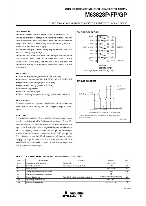
7.2k 3k
GND
The seven circuits share the COM and GND The diode, indicated with the dotted line, is parasitic, and cannot be used.
Unit : Ω
ABSOLUTE MAXIMUM RATINGS
q q q q q
PIN CONFIGURATION
IN1→ 1 IN2→ 2 IN3→ 3 INPUT IN4→ 4 IN5→ 5 IN6→ 6 IN7→ 7 GND
8 16 →O1 15 →O2 14 →O3 13 →O4 12 →O5 11 →O6 10 →O7 9
OUTPUT
→COM COMMON
Jan. 2000
元器件交易网
MITSUBISHI SEMICONDUCTOR <TRANSISTOR ARRAY>
M63823P/FP/GP
7-UNIT 500mA DARLINGTON TRANSISTOR-ARRAY WITH CLAMP DIODE
TYPICAL CHARACTERISTICS
M63823P/FP/GP
7-UNIT 500mA DARLINGTON TRANSISTOR-ARRAY WITH CLAMP DIODE
RECOMMENDED OPERATING CONDITIONS (Unless otherwise noted, Ta = –40 ~ +85°C)
Symbol VO Output voltage Collector current (Current per 1 circuit when 7 circuits are coming on simultaneously) Duty Cycle P : no more than 8% FP : no more than 5% GP : no more than 4% Duty Cycle P : no more than 30% FP : no more than 20% GP : no more than 15% IC ≤ 400mA IC ≤ 200mA Parameter Limits min 0 0 typ — — max 50 400 mA 0 3.85 3.4 0 — — — — 200 25 25 0.6 Unit V
- 1、下载文档前请自行甄别文档内容的完整性,平台不提供额外的编辑、内容补充、找答案等附加服务。
- 2、"仅部分预览"的文档,不可在线预览部分如存在完整性等问题,可反馈申请退款(可完整预览的文档不适用该条件!)。
- 3、如文档侵犯您的权益,请联系客服反馈,我们会尽快为您处理(人工客服工作时间:9:00-18:30)。
Surface Mount PIN Diodes Technical DataFeatures•Diodes Optimized for:Low Current SwitchingLow Distortion AttenuatingUltra-Low DistortionSwitchingMicrowave FrequencyOperation•Surface Mount SOT-23 and SOT-143 PackagesSingle and Dual VersionsTape and Reel OptionsAvailable•Low Failure in Time (FIT) Rate[1]Note:1.For more information see theSurface Mount PIN Reliability Data Sheet.HSMP-38XX andHSMP-48XX SeriesPackage Lead CodeIdentificationrequired. The HSMP-48XX seriesare special products featuringultra low parasitic inductance inthe SOT-23 package, specificallydesigned for use at frequencieswhich are much higher than theupper limit for conventionalSOT-23 PIN diodes. TheHSMP-4810 diode is a low distor-tion attenuating PIN designed foroperation to 3 GHz. TheHSMP-4820 diode is ideal forlimiting and low inductanceswitching applications up to1.5GHz. The HSMP-4890 isoptimized for low current switch-ing applications up to 3 GHz.The HSMP-386X series of generalpurpose PIN diodes are designedfor two classes of applications.The first is attenuators wherecurrent consumption is the mostimportant design consideration.The second application for thisseries of diodes is in switcheswhere low cost is the drivingissue for the designer.The HSMP-386X series TotalCapacitance (C T) and TotalResistance (R T) are typicalspecifications. For applicationsthat require guaranteed perfor-mance, the general purposeHSMP-383X series is recom-Description/Applications The HSMP-380X and HSMP-381X series are specifically designed for low distortion attenuator applica-tions. The HSMP-382X series is optimized for switching applica-tions where ultra-low resistance is required. The HSMP-3880 switch-ing diode is an ultra low distortion device optimized for higher power applications from 50 MHz to1.5GHz. The HSMP-389X series is optimized for switching applica-tions where low resistance at low attenuators, the HSMP-380X or -381X series are recommended. For high performance switching applications, the HSMP-389X series is recommended.A SPICE model is not available for PIN diodes as SPICE does not provide for a key PIN diode characteristic, carrier lifetime.Absolute Maximum Ratings [1] T A = 25°CSymbol ParameterUnits Absolute Maximum I f Forward Current (1 ms Pulse)Amp 1P t Total Device Dissipation mW [2]250P iv Peak Inverse Voltage —Same as V BRT j Junction Temperature °C 150T STGStorage Temperature°C-65 to 150Notes:1.Operation in excess of any one of these conditions may result in permanent damage to this device.2.CW Power Dissipation at T LEAD = 25°C. Derate to zero at maximum rated temperature.PIN Switching DiodesElectrical Specifications T A = 25°CNearest Maximum Equivalent Minimum Maximum Maximum Shunt Mode Part Package Axial Lead Breakdown Series Total Harmonic Number Marking LeadPart No.Voltage Resistance Capacitance Distortion HSMP-Code [1]Code Configuration 5082-V BR (V)R S (Ω)C T (pF)Hmd (dBc)3820F00Single 3188500.6*0.8*—3822F22Series3823F33Common Anode 3824F44Common Cathode 3880S00Single—100 6.50.40–553890G00Single —1002.50.30**—3892G22Series3893G33Common Anode 3894G44Common Cathode 3895G55Unconnected PairTest ConditionsV R = V BR I F = 5 mA V R = 50 V 2 f o, Z o = 50 W Measure f = 100 MHz f = 1 MHz f o = 400 MHz I R ≤ 10 µA I F = 10 mA*V R = 20 V*P in = +30 dBm V R = 5 V**0 V biasPIN Attenuator DiodesElectrical Specifications T A = 25°C (Each Diode)NearestEquivalent Minimum Maximum Maximum Minimum Maximum Part Package Axial Lead Breakdown Series Total High Low Number Marking LeadPart No.Voltage Resistance Capacitance Resistance Resistance HSMP-Code [1]Code Configuration 5082-V BR (V)R S (Ω)C T (pF)R H (Ω)R L (Ω)3800D00Single 30801002.00.37100083802D22Series3804D44Common Cathode 3810E00Single 3081100 3.00.351500103812E22Series3813E33Common Anode 3814E44Common CathodeTest ConditionsV R = V BR I F = 100 mA V R = 50 V I F = 0.01 mA I F = 20 mA Measure f = 100 MHz f = 1 MHz f = 100 MHz f= 100 MHzI R ≤ 10 µAPIN General Purpose Diodes, Electrical Specifications T A = 25°CNearestEquivalent Minimum Maximum Maximum Part Package Axial Lead Breakdown Series Total Number Marking Lead Part No.Voltage Resistance Capacitance HSMP-Code[1]Code Configuration5082-V BR (V)R S (Ω)C T (pF) 3830K00Single3077200 1.50.3 3832K22Series3833K33Common Anode3834K44Common CathodeTest Conditions V R = V BR I F = 100 mA V R = 50 VMeasure f = 100 MHz f = 1 MHzI R≤ 10 mAHigh Frequency (Low Inductance, 500 MHz – 3 GHz) PIN Diodes, Electrical Specifications T A = 25°CMinimum Maximum Typical Maximum TypicalBreak-Series Total Total Total Part Package down Resis-Capaci-Capaci-Induc-Number Marking Lead Config-Voltage tance tance tance tance Appli-HSMP-Code Code uration V BR (V)R S (Ω)C T (pF)C T (pF)L T (nH)cation 4810EB B Dual100 3.00.350.4 1.0Attenu-Cathode ator 4820FA A Dual Anode500.6*0.75* 1.0 1.0*Limiter 4890GA A Dual Anode100 2.5**0.330.375 1.0SwitchV R = V BR I F = 100 mA V R = 50 V V R = 50 V f = 500 MHz –Measure I F = 10 mA* f = 1 MHz f = 1 MHz 3 GHzI R≤ 10 µA I F = 5 mA**V R = 20 V*V R = 0 V V R = 20 V*PIN General Purpose Diodes, Typical Specifications T A = 25°CCode Minimum Typical Series Typical Total Part Number Marking Lead Breakdown Resistance Capacitance HSMP-Code[1]Code Configuration Voltage V BR (V)R S (Ω)C T (pF)3860L00Single50 3.0/1.5*0.203862L22Series3863L33Common Anode3864L44Common CathodeTest Conditions V R = V BR I F = 10 mA V R = 50 VMeasure f = 100 MHz f = 1 MHzI R≤ 10 µA*I F = 100 mATypical Parameters at T A = 25°CPart Number Series Resistance Carrier Lifetime Reverse Recovery Time Total Capacitance HSMP-R S (Ω)τ (ns)T rr (ns)C T (pF)380X5518005000.32 @ 50 V381X7515003000.27 @ 50 V382X 1.570*70.60 @ 20 V383X20500800.20 @ 50 V388X 3.825005500.30 @ 50 V389X 3.8200*–0.20 @ 5 V Test Conditions I F = 1 mA I F = 50 mA V R = 10 Vf = 100 MHz I R = 250 mA I F = 20 mAI F = 10 mA*I F = 10 mA*90% RecoveryI R = 6 mA*Typical Parameters at T A = 25°C (unless otherwise noted), Single DiodeFigure 2. RF Capacitance vs. Reverse Bias, HSMP-3830 Series.0.150.300.250.200.350.400.45T O T A L C A P A C I T A N C E (p F )REVERSE VOLTAGE (V)Figure 1. RF Capacitance vs. Reverse Bias, HSMP-3810 Series.Figure 3. Resistance at 25°C vs. Forward Bias Current.0.150.300.250.200.35T O T A L C A P A C I T A N C E (p F )REVERSE VOLTAGE (V)R E S I S T A N C E (O H M S )I F – FORWARD BIAS CURRENT (mA)0.010.11101000.010.1110100R F R E S I S T A N C E (O H M S )I F – FORWARD BIAS CURRENT (mA)R F R E S I S T A N C E (O H M S )0.010.1110100I F – FORWARD BIAS CURRENT (mA)Figure 5. RF Resistance vs. Forward Bias Current for HSMP-3810/HSMP-4810.V R – REVERSE VOLTAGE (V)C A P A C I T A N C E (p F )Figure 6. Capacitance vs. Reverse Voltage.Figure 4. RF Resistance vs. Forward Bias Current for HSMP-3800.100010010DIODE RF RESISTANCE (OHMS)Figure 7. 2nd Harmonic Input Intercept Point vs. Diode RFResistance for Attenuator Diodes.I N P U T I N T E R C E P T P O I N T (d B m )12011511010510095908511030I F – FORWARD BIAS CURRENT (mA)Figure 8. 2nd Harmonic Input Intercept Point vs. Forward Bias Current for Switch Diodes.I N P U T I N T E R C E P T P O I N T (d B m )FORWARD CURRENT (mA)Figure 9. Reverse Recovery Time vs. Forward Current for Various Reverse Voltages. HSMP-3820 Series.T r r – R E V E R S E R E C O V E R Y T I M E (n s )110100102030V R = 2V V R = 5VV R = 10VHSMP-382XTypical Parameters (continued)100010010102030T r r - R E V E R S E R E C O V E R Y T I M E (n S )FORWARD CURRENT (mA)Figure 10. Reverse Recovery Time vs. Forward Current for Various Reverse Voltage. HSMP-3830 Series.HSMP-3830V R = 5VV R = 10V V R = 20VR E V E R S E R E C O V E R Y T I M E (n S )FORWARD CURRENT (mA)Figure 11. Typical Reverse Recovery Time vs. Reverse Voltage. HSMP-3880 Series.1020152530T R R - R E V E R S E R E C O V E R Y T I M E (n S )FORWARD CURRENT (mA)Figure 12. Typical Reverse Recovery Time vs. Reverse Voltage. HSMP-3890 Series.1001010.10.01I F – F O R W A R D C U R R E N T (m A )I F – F O R W A R D C U R R E N T (m A )V F – FORWARD VOLTAGE (mA)Figure 14. Forward Current vs. Forward Voltage. HSMP-3810 and HSMP-4810 Series.V F – FORWARD VOLTAGE (mA)Figure 15. Forward Current vs. Forward Voltage. HSMP-3820 and HSMP-4820 Series.1001010.10.01I F – F O R W A R D C U R R E N T (m A )V F – FORWARD VOLTAGE (mA)Figure 16. Forward Current vs.Forward Voltage. HSMP-3830 Series.00.20.40.60.81.01.2I F – F O R W A R D C U R R E N T (m A )V F – FORWARD CURRENT (mA)Figure 17. Forward Current vs.Forward Voltage. HSMP-3880 Series.0.20.40.60.81.01.2V F – FORWARD VOLTAGE (mA)Figure 18. Forward Current vs. Forward Voltage. HSMP-3890 and HSMP-4890 Series.Typical Parameters (continued)Figure 19. Typical RF Resistance vs. Forward Bias Current for HSMP-3860.Figure 20. Forward Current vs. Forward Voltage for HSMP-3860.Figure 21. Typical Capacitance vs. Reverse Bias for HSMP-3860.10001R E S I S T A N C E (O HM S )BIAS CURRENT (mA)10100I F – F O R W A R D C U R R E N T (m A )V F – FORWARD VOLTAGE (V)0200.515C T – C A P A C I T A N C E (p F )V R – REVERSE VOLTAGE (V)0.20.41050.10.30.12 pF** Measured at -20 V C p 0.08 pFR j = 12ΩI 0.9C T = C P + C jI = Forward Bias Current in mAEquivalent Circuit ModelHSMS-3860Typical Applications for Multiple Diode ProductsRF COMMONRF 1RF 1Figure 24. Switch Using Both Positive and Negative Bias Current.Figure 25. Very High Isolation SPDT Switch, Dual Bias.Typical Applications for Multiple Diode Products (continued)INPUT RF IN/OUTFigure 26. Four Diode π Attenuator.Figure 27. High Isolation SPST Switch (Repeat Cells as Required).VOLTAGEBIASFigure 28. Power Limiter Using HSMP-3822Diode Pair.Typical Applications for HSMP-48XX Low Inductance SeriesFigure 29. Internal Connections.HSMP-4820 & HSMP-4890HSMP-48100.5 nH*0.8pF TYPICAL FOR HSMP-3820Figure 30. Equivalent Circuit.*0.8 pF TYPICAL FOR HSMP-3820Figure 32. Equivalent Circuit.Figure 31. Circuit Layout.Microstrip SeriesConnection for HSMP-48XX SeriesIn order to take full advantage of the low inductance of the HSMP-48XX series when using them in series application,both lead 1 and lead 2 should beconnected together, as shown above.Microstrip Shunt Connections for HSMP-48XX SeriesIn the diagram above, the center conductor of themicrostrip line is interrupted and leads 1 and 2 of theHSMP-38XX series diode are placed across the resulting gap. This forces the 0.5 nH lead inductance of leads 1 and 2 to appear as part of a low pass filter, reducing the shunt parasitic inductance andincreasing the maximumavailable attenuation. The 0.3 nH of shunt inductance external to the diode is created by the via holes, and is a good estimate for 0.032" thick material.Co-Planar Waveguide Shunt Connection for HSMP-48XX SeriesCo-Planar waveguide, with ground on the top side of the printed circuit board, is shownin the diagram above. Since it eliminates the need for via holes to ground, it offers lower shunt parasitic inductance and higher maximum attenuation whencompared to a microstrip circuit.GROUND BY TWOVIA HOLES*0.8 pF TYPICAL FOR HSMP-4820Figure 34. Equivalent Circuit.Figure 33. Circuit Layout.*0.8 pF TYPICAL FOR HSMP-4820Figure 36. Equivalent Circuit.Figure 35. Circuit Layout.11Package DimensionsOutline 23 (SOT-23)PC Board FootprintsSOT-23Package CharacteristicsLead Material......................................................................................Alloy 42Lead Finish............................................................................Tin-Lead 85-15%Maximum Soldering Temperature..............................260°C for 5 seconds Minimum Lead Strength..........................................................2 pounds pull Typical Package Inductance ..................................................................2 nH Typical Package Capacitance ..............................0.08 pF (opposite leads)SOT-143Outline 143 (SOT-143)SIDE VIEWEND VIEWDIMENSIONS ARE IN MILLIMETERS (INCHES)DIMENSIONS ARE IN MILLIMETERS (INCHES)PACKAGE MARKING/go/rfFor technical assistance or the location of your nearest Hewlett-Packard salesoffice, distributor or representative call:Americas/Canada: 1-800-235-0312 or 408-654-8675Far East/Australasia: Call your local HP sales office.Japan: (81 3) 3335-8152Europe: Call your local HP sales office.Data subject to change.Copyright © 1999 Hewlett-Packard Co.Obsoletes 5968-3435E5968-5439E (6/99)Profile Option Descriptions-BLK = Bulk-TR1 = 3K pc. Tape and Reel, Device Orientation; See Figures 37 and 38-TR2 = 10K pc. Tape and Reel, Device Orientation; See Figures 37 and 38Tape and Reeling conforms to Electronic Industries RS-481, “Taping of Surface Mounted Components for Automated Placement.”Ordering InformationSpecify part number followed by option under. For example:H SMP -38XX -XXXBulk or Tape and Reel OptionPart NumberSurface Mount PIN Diode Hewlett-PackardUSER FEEDEND VIEWTOP VIEW Figure 37. Options -TR1, -TR2 for SOT-23 Packages.Figure 38. Options -TR1, -TR2 for SOT-143 Packages.END VIEWTOP VIEW。