F-3401中文资料
全系列产品电子样本
上海奉申制冷控制器有限公司
MP45 系列小型压力控制器是一种用压力信号来控制的电开关,它是以压缩机的排气压力 为动作信号来控制压缩机的启停,当压缩机的排气压力超过调定值时,切断电源,起到压 力保护作用。
型号说明
型号
MP45
F
01
B
11
D
3
T
2.6
说明
型号代码 MP45M 为手动复 位形式
连接形式 代号 W
额定电压(V)
额定电流(A) 非诱导电流
诱导电流
满载电流 瞬时电流
A.C. 110
24 24 144
A.C.220
16 16 96
○1 : 公共触点 ○1 -○3 : 温度上升时闭合 ○1 -○5 :温度下降时闭合
↑M: 手动复位方向
版权归上海奉申制冷控制器有限公司所有,翻版必究! 网址:
自动
1.2 1.05
0.5→3.0 0.5→3.0
0.50~1.0 0.3~0.5
固定
自动 自动
2.0 1.5 2.0 1.5
0.5→3.0 固定≥0.4
手动
2.0 ≤1.6
0.3~0.5
0.5→3.0
自动 自动 0.3 0.2 2.0 1.5
固定
0.5→3.0 固定≥0.4 自动 手动 0.3 0.2 2.0 ≤1.6
标准附件及尺寸
版权归上海奉申制冷控制器有限公司所有,翻版必究! 网址:
压力控制器 P 系列
触点形式
形式
低压
型号 P2,P3,P6,P10
P6M
复位形式 自动 手动
P12D,P16D,P20D,P30D
自动
上海奉申制冷控制器有限公司
mos-3401
P-ChannelEnhancement Mode Power MOSFETPackage Marking and Ordering InformationDevice MarkingDevice Device PackageReel Size Tape width Quantity 34013401SOT-23Ø180mm8 mm3000 unitsAbsolute Maximum Ratings (T A =25℃unless otherwise noted)Parameter Symbol Limit UnitDrain-Source Voltage V DS -20 V Gate-Source VoltageV GS±12 V T C =25℃-3.8AT C =70℃ -3.2T A =25℃ -3 Continuous Drain CurrentT A =70℃I D-2.3A Drain Current -Pulsed (Note 1) I DM -15 A Maximum Power DissipationP D 1.7 W Operating Junction and Storage Temperature RangeT J ,T STG-55 To 150℃Thermal CharacteristicThermal Resistance,Junction-to-Ambient (Note 2)R θJA74/W ℃Electrical Characteristics (T A =25℃unless otherwise noted)ParameterSymbolConditionMin Typ MaxUnitOff CharacteristicsDrain-Source Breakdown Voltage BV DSS V GS =0V I D =-250μA -20 - - V Zero Gate Voltage Drain Current I DSS V DS =-20V,V GS =0V - - -1 μA Gate-Body Leakage Current I GSSV GS =±12V,V DS =0V -- ±100nAOn Characteristics (Note 3) Gate Threshold VoltageV GS(th) V DS =V GS ,I D =-250μA -0.45 -0.7 -1.0 VV GS =-4.5V, I D -39 52 Drain-Source On-State Resistance R DS(ON) V GS =-2.5V, I D=-3A - 58 75 m ΩForward Transconductance g FS V DS =-5V,I D =-2A 6- - S Dynamic Characteristics (Note4) Input Capacitance C lss - 490 - PFOutput CapacitanceC oss - 290 - PFReverse Transfer Capacitance C rssV DS =-4V,V GS =0V,F=1.0MHz- 190 - PF Switching Characteristics (Note 4) Turn-on Delay Time t d(on) - 12 - nSTurn-on Rise Time t r - 35 - nS Turn-Off Delay Time t d(off) - 30 - nSTurn-Off Fall Time t fV DD =-4V,I D =-3.3A , R L =-1.2Ω,V GEN =-4.5V,R g =1Ω- 10 - nSTotal Gate Charge Q g - 7.8 - nC Gate-Source Charge Q gs - 1.2 - nCGate-Drain ChargeQ gdV DS =-4V,I D =-4.1A,V GS =-4.5V - 1.6 - nCDrain-Source Diode Characteristics Diode Forward Voltage (Note 3) V SD V GS =0V,I S =-1.6A -- -1.2 V Diode Forward Current (Note 2)I S - - 1.6 ANotes:1. Repetitive Rating: Pulse width limited by maximum junction temperature.2. Surface Mounted on FR4 Board, t ≤ 10 sec.3. Pulse Test: Pulse Width ≤ 300μs, Duty Cycle ≤ 2%.4. Guaranteed by design, not subject to production=-3.5A。
PF3400电参数测量仪说明书
PF3400系列电参数测量仪(单相、三相三线制、三相四线制)用户使用手册杭州威博科技有限公司目录前言 (3)开箱检查 (4)安全警告事项 (5)标志说明 (6)第一章概述 (7)第二章技术指标 (8)第三章工作原理 (9)第四章前后面板主要功能 (12)第五章使用步骤 (20)第六章接线图集 (22)第七章检定或核准 (26)第八章注意事项 (27)第九章产品维护及常见故障排除 (27)前言感谢客户购置和使用杭州威博科技有限公司的产品,为保证安全、正确地使用本产品,敬请用户在操作之前详细阅读本用户使用手册的全部内容。
本用户使用手册适用于:PF3401,PF3402(带微打)PF340C,PF340B电参数测量仪本用户使用手册含有开箱检查、安全警告事项、产品的主要技术指标、工作原理、产品使用操作方法和常见故障处理等一系列内容。
在编写过程中,我们已经尽力确保本说明书内容的全面性和准确性。
如果用户在使用过程中有疑问,或者发现有不足和错误之处,欢迎直接与本司或本司授权的代理商进行联系。
用户对说明书如果有不同理解,以本司技术部的解释为准。
本用户使用手册的内容或个别地方可能发生改变,恕不另行通知。
请用户妥善保管本用户使用手册,不详之处可随时查阅,以保证仪器的正确使用。
没有本司书面许可,不得抄袭或改编本说明书的内容,否则被视为侵权。
开箱检查用户在打开产品的包装后,请取出装箱清单,并逐项检查清单所列内容与实物是否完全一致,并核对主机型号与你们的订购单是否相同,如果发现有不一致的地方,请与本司或本司授权的代理商联系。
所有的附件和文件,请妥善保管,以便日后的操作和维护之用。
本成套设备的配件和资料包括:1.PF3401或 PF3402或PF340C或PF340B电参数测量仪1台2.用户使用手册 1本3.产品合格证1份4.三芯电源线1根5.产品维修卡1份7.保险丝(0.5A)2只安全警告事项在使用本系列仪器的过程中必须注意下列安全规定,如不遵守本规定,产品功能可能受损并危及人身安全。
mos3401参数
mos3401的参数包括:
1.输出电压:5V
2.输出电流:2A
3.输入电压:2.5-5.5V
4.输入电压极性:正极性
5.工作温度范围:-20~+85℃
6.保护电路:过热保护、过流保护、过压保护、欠压保护
7.封装形式:SOT-23-3L
8.额定功率:5W
9.型号:MOS3401
10.应用范围:电机驱动、电源转换、电源管理、通信电源等
11.类型:MOSFET
12.电压调节率:0.1% typ
13.输出电压漂移:±5% typ
14.栅极阈值电压:±1V typ
15.输入电容:10pF typ
16.输出电容:22pF typ
17.工作温度:-20°C to +85°C (TA)
18.工作电压范围:2.5V to 5.5V (VS)
19.最大漏源电压:30V
20.最大栅源电压:±10V
21.最小栅极驱动电压:±3V typ
22.最大漏极电流:-40A typ, -30A typ(with VS=5V)
23.最大栅极电阻:4kΩ typ
24.导通电阻(Drain Source导通电阻):RDS(ON)=4mΩ typ(VS=3V, ID=-40A)
25.导通电阻(Drain Source导通电阻):RDS(ON)=8mΩ typ(VS=5V, ID=-40A)。
SI3400中文资料
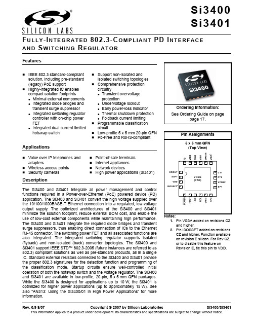
Rev. 0.9 8/07Copyright © 2007 by Silicon LaboratoriesSi3400/Si3401This information applies to a product under development. Its characteristics and specifications are subject to change without notice.Si3400Si3401F U L L Y -I N T EG R A T E D 802.3-C O M P L I A N T PD I N T E R F A C E A N D S W I T CHI N G R E G U L A T O RFeaturesApplicationsDescriptionThe Si3400 and Si3401 integrate all power management and control functions required in a Power-over-Ethernet (PoE) powered device (PD)application. The Si3400 and Si3401 convert the high voltage supplied over the 10/100/1000BASE-T Ethernet connection into a regulated, low-voltage output supply. The optimized architectures of the Si3400 and Si3401minimize the solution footprint, reduce external BOM cost, and enable the use of low-cost external components while maintaining high performance.The Si3400 and Si3401 integrate the required diode bridges and transient surge suppressors, thus enabling direct connection of ICs to the Ethernet RJ-45 connector. The switching power FET and all associated functions are also integrated. The integrated switching regulator supports isolated (flyback) and non-isolated (buck) converter topologies. The Si3400 and Si3401 support IEEE STD™ 802.3-2005 (future instances are referred to as 802.3) compliant solutions as well as pre-standard products, all in a single IC. Standard external resistors connected to the Si3400 and Si3401 provide the proper 802.3 signatures for the detection function and programming of the classification mode. Startup circuits ensure well-controlled initial operation of both the hotswap switch and the voltage regulator. The Si3400and Si3401 are available in low-profile, 20-pin, 5x 5mm QFN packages.While the Si3400 is designed for applications up to 10W, the Si3401 is optimized for higher power applications (up to approximately 15W). See also “AN313: Using the Si3400/01 in High Power Applications” for more information.IEEE 802.3 standard-compliant solution, including pre-standard (legacy) PoE supportHighly-integrated IC enables compact solution footprintsMinimal external components Integrated diode bridges and transient surge suppressor Integrated switching regulator controller with on-chip power FETIntegrated dual current-limited hotswap switchSupport non-isolated and isolated switching topologiesComprehensive protection circuitryTransient overvoltage protectionUndervoltage lockoutEarly power-loss indicator Thermal shutdown protection Foldback current limiting Programmable classification circuitLow-profile 5x 5mm 20-pin QFNPb-Free and RoHS-compliantVoice over IP telephones and adaptersWireless access points Security camerasPoint-of-sale terminals Internet appliances Network devicesHigh power applications (Si3401)1.Pin VSSA added on revisions CZand higher.2. Pin ISOSSFT added on revisionsCZ and higher. Function available on revision E silicon. For Rev CZ, or to disable this feature on Revision E, tie this pin to VDD.Ordering Information:See Ordering Guide on pagepage 17.元器件交易网Si3400/Si34012Rev. 0.9Functional Block DiagramSi3400/Si3401Rev. 0.93T A B L E O F C O N T E N TSSectionPage1. Electrical Specifications . . . . . . . . . . . . . . . . . . . . . . . . . . . . . . . . . . . . . . . . . . . . . . . . . . .42. Typical Application Schematics . . . . . . . . . . . . . . . . . . . . . . . . . . . . . . . . . . . . . . . . . . . . .83. Functional Description . . . . . . . . . . . . . . . . . . . . . . . . . . . . . . . . . . . . . . . . . . . . . . . . . . .103.1. Overview . . . . . . . . . . . . . . . . . . . . . . . . . . . . . . . . . . . . . . . . . . . . . . . . . . . . . . . . . .103.2. PD Hotswap Controller . . . . . . . . . . . . . . . . . . . . . . . . . . . . . . . . . . . . . . . . . . . . . . .103.3. Switching Regulator . . . . . . . . . . . . . . . . . . . . . . . . . . . . . . . . . . . . . . . . . . . . . . . . .134. Pin Descriptions . . . . . . . . . . . . . . . . . . . . . . . . . . . . . . . . . . . . . . . . . . . . . . . . . . . . . . . . .155. Package Outline . . . . . . . . . . . . . . . . . . . . . . . . . . . . . . . . . . . . . . . . . . . . . . . . . . . . . . . . .166. Ordering Guide . . . . . . . . . . . . . . . . . . . . . . . . . . . . . . . . . . . . . . . . . . . . . . . . . . . . . . . . . .17Document Change List . . . . . . . . . . . . . . . . . . . . . . . . . . . . . . . . . . . . . . . . . . . . . . . . . . . . .18Contact Information . . . . . . . . . . . . . . . . . . . . . . . . . . . . . . . . . . . . . . . . . . . . . . . . . . . . . . . .20Si3400/Si34014Rev. 0.91. Electrical SpecificationsTable 1. Absolute Maximum Ratings (DC)1Type DescriptionRating UnitVoltageCT1 to CT2–60 to 60V SP1 to SP2–60 to 60VPOS 2–0.3 to 60HSO–0.3 to 60VSS1 or VSS2–0.3 to 60SWO–0.3 to 60PLOSS to VPOS 2–60 to 0.3RDET –0.3 to 60RCL–0.3 to 5SSFT to VPOS 2–5 to 0.3EROUT to VSS1, VSS2, or VSSA –0.3 to VDD+0.3FB to VPOS–5 to 0.3RIMAX to VSS1, VSS2, or VSSA –0.3 to VDD+0.3VSS1 to VSS2 or VSSA –0.3 to 0.3VDD to VSS1, VSS2, or VSSA–0.3 to 5CurrentRCL 0 to 100mA RDET0 to 1CT1, CT2, SP1, SP2–400 to 400VPOS 2–400 to 400HSO 0 to 400PLOSS –0.5 to 5VDD 0 to 2SWO0 to 400VSS1, VSS2, or VSSA–400 to 0Ambient TemperatureStorage –65 to 150°C Operating–40 to 85Notes:1.Unless otherwise noted, all voltages referenced to VNEG. Permanent device damage may occur if the maximum ratingsare exceeded. Functional operation should be restricted to those conditions specified in the operational sections of this data sheet. Exposure to absolute maximum rating conditions for extended periods may adversely affect device reliability.2. VPOS is equal to VPOSF and VPOSS tied together for test condition purposes.Si3400/Si3401Rev. 0.95Table 2. Absolute Maximum Ratings (Transient)1Transient surge defined in IEC60060 as a 1000V impulse of either polarity applied across CT1–CT2 or SP1–SP2. The shape of the impulse shall have a 300ns full rise time and a 50µs half fall time, with 201Ω source impedance.Type Description Rating UnitVoltageCT1 to CT2–82 to 82VSP1 to SP2–82 to 82VPOS 2–0.7 to 80HSO–0.7 to 80VSS1, VSS2, or VSSA –0.7 to 80SWO–0.7 to 80PLOSS to VPOS 2–80 to 0.7RDET–0.7 to 80CurrentCT1, CT2, SP1, SP2–5 to 5A VPOS 2–5 to 5ESD 3HBM, all pins–2 to 2kVNotes:1.Unless otherwise noted, all voltages referenced to VNEG. Permanent device damage may occur if the maximum ratingsare exceeded. Functional operation should be restricted to those conditions specified in the operational sections of this data sheet. Exposure to absolute maximum rating conditions for extended periods may adversely affect device reliability.2. VPOS is equal to VPOSF and VPOSS tied together for test condition purposes.3. For more information regarding system-level ESD tolerance, refer to “AN315: Robust Electrical Surge Immunity for PoEPDs through Integrated Protection”.Table 3. Recommended Operating ConditionsDescriptionSymbol Min Typ Max Units |CT1–CT2| or |SP1–SP2|VPORT 2.8—57V Ambient Operating TemperatureTA–402585°CNote:Unless otherwise noted, all voltages referenced to VNEG. All minimum and maximum specifications are guaranteedand apply across the recommended operating conditions. Typical values apply at nominal supply voltage and ambient temperature unless otherwise noted.Si3400/Si34016Rev. 0.9Table 4. Electrical CharacteristicsParameter Description Min Typ Max UnitVPORTDetection 2.7—11V Classification14—22UVLO Turn Off——42UVLO Turn On30—36 Transient Surge162—79Input Offset Current VPORT < 10V——10µA Diode bridge leakage VPORT=57V——25µAIPORT Classification2Class 00—4mA Class 19—12Class 217—20Class 326—30Class 436—44IPORT Operating Current336V<VPORT<57V—2 3.1mACurrent Limit4Inrush—130— mA Operating350 (Si3400)470 (Si3401)525550—mAHotswap FET On-Resistance +R SENSE36V<VPORT<57V0.5— 1.4ΩPower loss VPORT Threshold273033V Switcher Frequency—350—kHzMaximum Switcher Duty Cycle5ISOSSFT connected toVDD —50—%Switching FET On-Resistance0.3—0.86ΩRegulated Feedback @ pin FB6DC Avg.— 1.23—VRegulated Output Voltage Tolerance6Output voltage tolerance @VOUT –5—5%Notes:1.Transient surge defined in IEC60060 as a 1000V impulse of either polarity applied to CT1–CT2 or SP1–SP2. Theshape of the impulse shall have a 300ns full rise time and a 50µs half fall time with 201Ω source impedance.2. The classification currents are guaranteed only when recommended RCLASS resistors are used, as specified inTable10.3. IPORT includes full operating current of switching regulator controller.4. The PD interface includes dual-level input current limit. At turn-on, before the HSO load capacitor is charged, thecurrent limit is set at the inrush level. After the capacitor has been charged within ~1.25V of VNEG, the operating current limit is engaged. This higher current limit remains active until the UVLO lower limit has been tripped or until the hotswap switch is sufficiently current-limited to cause a foldback of the HSO voltage.5. See “AN296: Using the Si3400/01 PoE PD Controller in Isolated and Non-Isolated Designs” for more information.6. Applies to non-isolated applications only (VOUT on schematic in Figure1).Si3400/Si3401Rev. 0.97VDD accuracy @ 0.8mA 36V <VPORT <57V4.5—5.5V Softstart charging current —12—µA Thermal ShutdownJunction temperature—160—ºC Thermal Shutdown Hysteresis——25ºCTable 5. Total Power DissipationDescription ConditionMin Typ Max Units Power Dissipation VPORT =50V, V OUT =5V, 2A— 1.2—W Power Dissipation*VPORT =50V, V OUT =5V, 2A w/ diode bridges bypassed—0.7—W*Note: Silicon Laboratories recommends the on-chip diode bridges be bypassed when output power requirements are >10W(Si3401) or in thermally-constrained applications. For more information, see “AN313: Using the Si3400 and Si3401 in High Power Applications”.Table 6. Package Thermal CharacteristicsParameterSymbol Test ConditionTyp Units Thermal resistance (junction to ambient)θJAStill air; assumes a minimum of nine thermal vias are connected to a 2in 2 heat spreader plane for the package “pad” node (VNEG).44°C/WTable 4. Electrical Characteristics (Continued)ParameterDescription Min Typ Max Unit Notes:1.Transient surge defined in IEC60060 as a 1000V impulse of either polarity applied to CT1–CT2 or SP1–SP2. Theshape of the impulse shall have a 300ns full rise time and a 50µs half fall time with 201Ω source impedance.2. The classification currents are guaranteed only when recommended RCLASS resistors are used, as specified inTable 10.3. IPORT includes full operating current of switching regulator controller.4. The PD interface includes dual-level input current limit. At turn-on, before the HSO load capacitor is charged, thecurrent limit is set at the inrush level. After the capacitor has been charged within ~1.25V of VNEG, the operatingcurrent limit is engaged. This higher current limit remains active until the UVLO lower limit has been tripped or until the hotswap switch is sufficiently current-limited to cause a foldback of the HSO voltage.5. See “AN296: Using the Si3400/01 PoE PD Controller in Isolated and Non-Isolated Designs” for more information.6. Applies to non-isolated applications only (VOUT on schematic in Figure 1).Si3400/Si34018Rev. 0.92. Typical Application SchematicsFigure1.Schematic—Class 0 with Non-Isolated 5V Output**Note:This is a simplified schematic. See “AN296: Using the Si3400/01 PoE PD Controller in Isolated and Non-Isolated Designs” for more details and complete application schematics.Table 7. Component Listing—Class 0 with 5V OutputItem Type Value Toler.Rating NotesC1Capacitor15µF20%100V Switcher supply capacitor. Several paral-lel capacitors are used for lower ESR.C2Capacitor0.1µF20%100V PD input supply capacitor.C3Capacitor1000µF20%10V Switcher load capacitor - 1000µF in par-allel with and X5R 22µF for lower ESR.C4Capacitor0.1µF20%16V VDD bypass capacitor.C5Capacitor0.1µF10%16V Softstart capacitor.C6Capacitor 3.3nF10%16V Compensation capacitor.C7Capacitor150pF10%16V Compensation capacitor.R1Resistor25.5kΩ1%1/16W Detection resistor.R2Resistor7.32kΩ1%1/16W Feedback resistor divider.R3Resistor 2.87kΩ1%1/16W Feedback resistor divider.R4Resistor30.1kΩ1%1/16W Feedback compensation resistor.D1Diode100V Schottky diode; part no. PDS5100.L1Inductor33µH20% 3.5A Coilcraft part no. DO5010333.Si3400/Si3401Rev. 0.99Figure 2.Schematic—Class 1 with Isolated 5.0V Output**Note: This is a simplified schematic. See “AN296: Using the Si3400/01 PoE PD Controller in Isolated and Non-IsolatedDesigns” for more details and complete application schematics.Table 8. Components—Class 1 with Isolated 5.0V OutputItem Type Value Toler.Rating NotesC1Capacitor 15µF 20%100V Switcher supply capacitor. Several paral-lel capacitors are used for lower ESR.C2Capacitor 0.1µF 20%100V PD input supply capacitor.C3Capacitor1100µF20%10VSwitcher load capacitor. 100µF in parallel 1000µF and optional 1µH inductor for additional filtering.C4Capacitor 15nF 10%16V Feedback compensation.C5Capacitor 220nF 10%16V Feedback compensation.C7Capacitor 0.1µF 20%16V VDD bypass capacitor.C8Capacitor 1µF 20%16V Isolated mode soft start (tie ISOSSFT to VDD if this feature is not used).R1Resistor 25.5k Ω1%1/16W Detection resistor.R2Resistor 4.99k Ω1%1/16W Pull-up resistor.R3Resistor 100Ω1%1/16W Feedback compensation resistor.R4Resistor 10k Ω1%1/16W Feedback compensation resistor.R5Resistor 2.05k Ω1%1/16W Pull-up resistor.R6Resistor 36.5k Ω1%1/16W Feedback resistor divider.R7Resistor 12.1k Ω1%1/16W Feedback resistor divider.R8Resistor 127Ω1%1/16W Classification resistor.D1Diode 10A 40V Schottky diode; part no. PN PDS1040.D2Diode 1A 100V Snubber diode (1N4148)D3Diode 15V 9ASnubber diode (DFLT15A)T1Transformer 40µHCoilcraft part number FA2672 (5V).PS2911Optocoupler TLV431Voltage referenceSi3400/Si340110Rev. 0.93. Functional DescriptionThe Si3400 and Si3401 consist of two major functions: a hotswap controller/interface and a complete pulse-width-modulated switching regulator (controller and power FET).3.1. OverviewThe hotswap interfaces of the Si3400 and Si3401 provide the complete front end of an 802.3-compliant PD. The Si3400 and Si3401 also include two full diode bridges, a transient voltage surge suppressor, detection circuit, classification current source, and dual-level hotswap current limiting switch. This high level of integration enables direct connection to the RJ-45 connector, simplifies system design, and provides significant advantages for reliability and protection. The Si3400 and Si3401 require only four standard external components (detection resistor, optional classification resistor, load capacitor, and input capacitor) to create a fully 802.3-compliant interface. For more information about supporting higher-power applications, see “AN313: Using the Si3400 and Si3401 in High Power Applications” and “AN314: Power Combining Circuit for PoE for up to 18.5W Output”.The Si3400 and Si3401 integrate a complete pulse-width modulated switching regulator that includes the controller and power FET. The switching regulator utilizes a constant frequency pulse-width modulated controller optimized for all possible load conditions in PoE applications. The regulator integrates a low on-resistance (Ron) switching power MOSFET that minimizes power dissipation, increases overall regulator efficiency, and simplifies system design. An integrated error amplifier, precision reference, and programmable soft-start current source provide the flexibility of using a non-isolated buck regulator topology or an isolated flyback regulator topology.The Si3400 and Si3401 are designed to operate with both 802.3-compliant Power Sourcing Equipment (PSE) and pre-standard (legacy) PSEs that do not adhere to the 802.3 specified inrush current limits. The Si3400 and Si3401 are compatible with compliant and legacy PSEs because they use two levels for the hotswap current limits. By setting the initial inrush current limit to a low level, a PD based on the Si3400 or Si3401 minimizes the current drawn from either a compliant or legacy PSE during startup. After powering up, the Si3400 and Si3401 automatically switch to a higher-level current limit, thereby allowing the PD to consume up to 12.95W (the max power allowed by the 802.3 specification).The inrush current limit specified by the 802.3 standard can generate high transient power dissipation in the PD. By properly sizing the devices and implementing on-chip thermal protection, the Si3400 and Si3401 can go through multiple turn-on sequences without overheating the package or damaging the device. The switching regulator power MOSFET has been conservatively designed and sized to withstand the high peak currents created when converting a high-voltage, low-current supply into a low-voltage, high-current supply. Excessive power cycling or short circuit faults will engage the thermal overload protection to prevent the onboard power MOSFETs from exceeding their safe and reliable operating ranges.3.2. PD Hotswap ControllerThe Si3400 and Si3401 hotswap controllers change their mode of operation based on the input voltage applied to the CT1 and CT2 pins or the SP1 and SP2 pins, the 802.3-defined modes of operation, and internal controller requirements. Table9 defines the modes of operation for the hotswap interface.3.2.1. Rectification Diode Bridges andSurge SuppressorThe 802.3 specification defines the input voltage at the RJ-45 connector of the PD with no reference to polarity. In other words, the PD must be able to accept power of either polarity at each of its inputs. This requirement necessitates the use of two sets of diode bridges, one for the CT1 and CT2 pins and one for the SP1 and SP2 pins to rectify the voltage. Furthermore, the standard requires that a PD withstand a high-voltage transient surge consisting of a 1000V common-mode impulse with 300ns rise time and 50µs half fall time. Typically, the diode bridge and the surge suppressor have been implemented externally, adding cost and complexity to the PD system design.The diode bridge* and the surge suppressor have been integrated into the Si3400 and Si3401, thus reducing system cost and design complexity.*Note:Silicon Laboratories recommends that on-chip diode bridges be bypassed when >10W of output power isrequired.By integrating the diode bridges, the Si3400 and Si3401 gain access to the input side of the diode bridge. Monitoring the voltage at the input of the diode bridges instead of the voltage across the load capacitor provides the earliest indication of a power loss. This true early power loss indicator, PLOSS, provides a local microcontroller time to save states and shut down gracefully before the load capacitor discharges below the minimum 802.3-specified operating voltage of 36V. Integration of the surge suppressor enables optimization of the clamping voltage and guarantees protection of all connected circuitry.As an added benefit, the transient surge suppressor, when tripped, actively disables the hotswap interface and switching regulator, preventing downstream circuits from encountering the high-energy transients.3.2.2. DetectionIn order to identify a device as a valid PD, a PSE will apply a voltage in the range of 2.8V to 10V on the cable and look for the 25.5kΩ signature resistor. The Si3400 and Si3401 will react to voltages in this range by connecting an external 25.5kΩ resistor between VPOS and VNEG. This external resistor and internal low-leakage control circuitry create the proper signature to alert the PSE that a valid PD has been detected and is ready to have power applied. The internal hotswap switch is disabled during this time to prevent the switching regulator and attached load circuitry from generating errors in the detection signature.Since the Si3400 and Si3401 integrate the diode bridges, the IC can compensate for the voltage and resistance effects of the diode bridges. The 802.3 specification requires that the PSE use a multi-point,∆V/∆I measurement technique to remove the diode-induced dc offset from the signature resistance measurement. However, the specification does not address the diode's nonlinear resistance and the error induced in the signature resistor measurement. Since the diode's resistance appears in series with the signature resistor, the PD system must find some way of compensating for this error. In systems where the diode bridges are external, compensation is difficult and suffers from errors. Since the diode bridges are integrated in the Si3400 and Si3401, the IC can easily compensate for this error by offsetting resistance across all operating conditions and thus meeting the 802.3 requirements. An added benefit is that this function can be tested during the IC’s automated testing step, guaranteeing system compliance when used in the final PD application. For more information about supporting higher-power applications (above 12.95W), see “AN313: Using the Si3400 and Si3401 in High Power Applications” and “AN314: Power Combining Circuit for PoE for up to 18.5W Output”.3.2.3. ClassificationOnce the PSE has detected a valid PD, the PSE may classify the PD for one of five power levels or classes. A class is based on the expected power consumption of the powered device. An external resistor sets the nominal class current that can then be read by the PSE to determine the proper power requirements of the PD. When the PSE presents a fixed voltage between 15.5V and 20.5V to the PD, the Si3400 and Si3401 assert the class current from VPOS through the RCL resistor.Table 9. Hotswap Interface ModesInput Voltage (|CT1-CT2| or |SP1-SP2|)Si3400 and Si3401Mode0V to 2.7V Inactive2.7V to 11V Detection signature11V to 14V Detection turns off andinternal bias starts 14V to 22V Classification signature22V to 42V Transition region42V up to 57V Switcher operating mode(hysteresis limit based onrising input voltage)57V down to 36V Switcher operating mode(hysteresis limit based onfalling input voltage)The resistor values associated with each class are shown in Table10.The 802.3 specification limits the classification time to 75ms to limit the power dissipated in the PD. If the PSE classification period exceeds 75ms and the die temperature rises above the thermal shutdown limits, the thermal protection circuit will engage and disable the classification current source in order to protect the Si3400 and Si3401. The Si3400 and Si3401 stay in classification mode until the input voltage exceeds 22V (the upper end of its classification operation region). 3.2.4. Under Voltage LockoutThe 802.3 standard specifies the PD to turn on when the line voltage rises to 42V and for the PD to turn off when the line voltage falls to 30V. The PD must also maintain a large on-off hysteresis region to prevent wiring losses between the PSE and the PD from causing startup oscillation.The Si3400 and Si3401 incorporate an undervoltage lockout (UVLO) circuit to monitor the line voltage and determine when to apply power to the integrated switching regulator. Before the power is applied to the switching regulator, the hotswap switch output (HSO) pin is high-impedance and typically follows VPOS as the input is ramped (due to the discharged switcher supply capacitor). When the input voltage rises above the UVLO turn-on threshold, the Si3400 and Si3401 begin to turn on the internal hotswap power MOSFET. The switcher supply capacitor begins to charge up under the current limit control of the Si3400 and Si3401, and the HSO pin transitions from VPOS to VNEG. The Si3400 and Si3401 include hysteretic UVLO circuits to maintain power to the load until the input voltage falls below the UVLO turn-off threshold. Once the input voltage falls below 30V, the internal hotswap MOSFET is turned off.3.2.5. Dual Current Limit and Switcher Turn-OnThe Si3400 and Si3401 implement dual current limits. While the hotswap MOSFET is charging the switcher supply capacitor, the Si3400 and Si3401 maintain a low current limit. The switching regulator is disabled until the voltage across the hotswap MOSFET becomes sufficiently low, indicating the switcher supply capacitor is almost completely charged. When this threshold is reached, the switcher is activated, and the hotswap current limit is increased. This threshold also has hysteresis to prevent systemic oscillation as the switcher begins to draw current and the current limit is increased, which allows resistive losses in the cable to effectively decrease the input supply.The Si3400 and Si3401 stay in a high-level current limit mode until the input voltage drops below the UVLO turn-off threshold or excessive power is dissipated in the hotswap switch. This dual level current limit allows the system designer to design powered devices for use with both legacy and compliant PoE systems.An additional feature of the dual current limit circuitry is foldback current limiting in the event of a fault condition. When the current limit is switched to the higher level, 400mA of current can be drawn by the PD. Should a fault cause more than this current to be consumed, the voltage across the hotswap MOSFET will increase to clamp the maximum amount of power consumed. The power dissipated by the MOSFET can be very high under this condition. If the fault is very low impedance, the voltage across the hotswap MOSFET will continue to rise until the lower current limit level is engaged, further reducing the dissipated power. If the fault condition remains, the thermal overload protection circuitry will eventually engage and shut down the hotswap interface and switching regulator. The foldback current limiting occurs much faster than the thermal overload protection and is, therefore, necessary for comprehensive protection of the hotswap MOSFET.Table 10. Class Resistor ValuesClass Usage Power Levels Nominal ClassCurrent RCL Resistor (1%,1/16W)0Default0.44W to 12.95W< 4mA> 1.33kΩ(or open circuit) 1Optional0.44W to 3.84W10.5mA127Ω2Optional 3.84W to 6.49W18.5mA69.8Ω3Optional 6.49W to 12.95W28mA45.3Ω4Reserved Reserved40mA30.9Ω3.2.6. Power Loss IndicatorA situation can occur in which power is lost at the input of the diode bridge and the hotswap controller does not detect the fault due to the VPOS to VNEG capacitor maintaining the voltage. In such a situation, the PD can remain operational for hundreds of microseconds despite the PSE having removed the line voltage. If it is recognized early enough, the time from power loss to power failure can provide valuable time to gracefully shut down an application.Due to integration of the diode bridges, the Si3400 and Si3401 are able to instantaneously detect the removal of the line voltage and provide that early warning signal to the PD application. The PLOSS pin is an open drain output that pulls up to VPOS when a line voltage greater than 27V is applied. When the line voltage falls below 27V, the output becomes high-impedance, allowing an external pull-down resistor to change the logic state of PLOSS. The benefit of this indicator is that the powered device may include a microcontroller that can quickly save its memory or operational state before draining the supply capacitors and powering itself down. This feature can help improve overall manageability in applications, such as wireless access points.3.3. Switching RegulatorPower over Ethernet (PoE) applications fall into two broad categories, isolated and non-isolated. Non-isolated systems can be used when the powered device is self-contained and does not provide external conductors to the user or another application. Non-isolated applications include wireless access points and security cameras. In these applications, there is no explicit need for dc isolation between the switching regulator output and the hotswap interface. An isolated system must be used when the powered device interfaces with other self-powered equipment or has external conductors accessible to the user or other applications. For proper operation, the regulated output supply of the switching regulator must not have a dc electrical path to the hotswap interface or switching regulator primary side. Isolated applications include point-of-sale terminals where the user can touch the grounded metal chassis.The application determines the converter topology. An isolated application will require a flyback transformer-based switching topology while a non-isolated application can use an inductor-based buck converter topology. In the isolated case, dc isolation is achieved through a transformer in the forward path and a voltage reference plus opto-isolator in the feedback path. The application circuit shown in Figure2 is an example of such a topology. The non-isolated application in Figure1 makes use of a single inductor as the energy conversion element, and the feedback signal is directly supplied into the internal error amplifier. As can be seen from the application circuits, the isolated topology has an increased number of components, thus increasing the bill of materials (BOM) and system footprint.To optimize cost and ease implementation, each application should be evaluated for its isolated or non-isolated requirements.。
RF3401M蓝牙对讲模块说明书_V3
RF3401M模块的说明书RF3401M模块功能简介1、支持蓝牙音频发射和接收主机可以连接市面上的蓝牙耳机或者蓝牙音箱从机可以连接手机播放音乐2、支持蓝牙对讲连接市面上的蓝牙耳机实现全双工的对讲,兼容性在50%3、支持主机和从机之间,互相连接,实现音频无线传输。
由主机发送给从机。
同时双向对讲4、支持主机和从机之间,互相连接,实现数据透传通过串口的方式5、支持一些功能的操作全部AT串口指令完成6、支持芯片出货或者模块出货都很灵活QSOP24封装、QFN32封装,根据不同需求来选择7、软硬件自己开发,所以非常灵活定制出各种需求的产品一、问题集锦问题1为什么模块要成对卖呢?不能单独买一个主机去连接我的蓝牙耳机吗?答疑1、因为蓝牙双向对讲,存在很严重的兼容性的问题,只有成对卖,我们的售后才会少2、因为成对之后,主机和从机之间,是效果非常好的,能记忆连接,能成功发起对讲3、也可以单独用其中的一个,去连接市面上的蓝牙耳机,但是兼容性只有50%左右。
并且技术上面是不能做到很高的兼容率。
如果遇到不支持的耳机,请不要试图要求我们解决,解决不了的。
请知晓基本不支持市面上QCC、CSR系列的蓝牙耳机,支持杰理、建荣、蓝汛的芯片方案的耳机,要测试才知道问题2如何连接蓝牙耳机或者音箱呢?连接成功之后延时怎么样?车载蓝牙可以连接吗?支持一对多吗?答疑1、可以的,模块作为发射时【也就是主机】。
就和您用的手机一样,能去搜索从机设备[蓝牙耳机、蓝牙音箱]2、并且建立连接,然后发射模块把音频发射给从机设备。
注意一定要切换到主机模式【红灯超快闪】3、延时大概在300ms左右。
并且会随着从机设备的不同,而不同4、不支持车载蓝牙的连接。
不支持一对多,只支持一对一5、模块是单声道,就是不分立体声。
左右耳朵的声音是一样的。
一般普通的应用也不需要立体声的,请知晓。
MSP3401摩矽MOS管
MSP3401● V DS = -30V,I D = -4.2A R DS(ON) < 130m Ω @ V GS =-2.5V R DS(ON) < 75m Ω @ V GS =-4.5V R DS(ON) < 55m Ω @ V GS =-10V● High power and current handing capability ● Lead free product is acquired ● Surface mount package●PWM applications ●Load switch ●Power managementSchematic diagramMarking and Pin AssignmentSOT-23 top viewPackage Marking And Ordering InformationDevice MarkingDevice Device PackageReel Size Tape width Quantity MSP3401SOT-23Ø180mm8 mm3000 unitsAbsolute Maximum Ratings (TA=25℃unless otherwise noted)Parameter Symbol Limit UnitDrain-Source Voltage V DS -30 V Gate-Source VoltageV GS ±12 V Drain Current-Continuous I D -4.2 A Drain Current-Pulsed (Note 1) I DM-30 A Maximum Power Dissipation P D 1.2 W Operating Junction and Storage Temperature Range T J ,T STG -55 To 150 ℃Thermal CharacteristicThermal Resistance,Junction-to-Ambient (Note 2)R θJA104 /W ℃-30V(D-S) P-Channel Enhancement Mode Power MOS FETLead FreePIN ConfigurationGeneral FeaturesApplicationGate-Body Leakage Current I GSSV GS =±10V,V DS =0V - - ±100nAOn Characteristics (Note 3) Gate Threshold VoltageV GS(th) V DS =V GS ,I D =-250μA -0.7 -1 -1.3 V V GS =-10V, I D =-4.2A - 50 55 m ΩV GS =-4.5V, I D =-4A - 64 75 m Ω Drain-Source On-State ResistanceR DS(ON)V GS =-2.5V, I D =-1A95 130 m Ω Forward Transconductance g FSV DS =-5V,I D =-4.2A - 10 - SDynamic Characteristics (Note4) Input Capacitance C lss - 950 - PF Output CapacitanceC oss - 115 - PFReverse Transfer Capacitance C rssV DS =-15V,V GS =0V,F=1.0MHz- 75 - PF Switching Characteristics (Note 4) Turn-on Delay Time t d(on) - 7 - nSTurn-on Rise Time t r - 3 - nS Turn-Off Delay Time t d(off) - 30 - nSTurn-Off Fall Time t fV DD =-15V,I D =-3.2A V GS =-10V,R GEN =6Ω - 12 - nSTotal Gate Charge Q g - 9.5 - nC Gate-Source Charge Q gs - 2 - nCGate-Drain ChargeQ gdV DS =-15V,I D =-4A,V GS =-4.5V - 3 - nCDrain-Source Diode Characteristics Diode Forward Voltage (Note 3)V SDV GS =0V,I S =-1A - - -1.2 VNotes:1. Repetitive Rating: Pulse width limited by maximum junction temperature.2. Surface Mounted on FR4 Board, t ≤ 10 sec.3. Pulse Test: Pulse Width ≤ 300μs, Duty Cycle ≤ 2%.4. Guaranteed by design, not subject to productionElectrical Characteristics (TA=25℃unless otherwise noted)ParameterSymbol Condition Min Typ Max UnitOff CharacteristicsDrain-Source Breakdown Voltage BV DSS V GS =0V I D =-250μA -30 - V Zero Gate Voltage Drain Current I DSS V DS =-24V,V GS =0V - - -1 μATypical Electrical and Thermal CharacteristicsFigure 1:Switching Test CircuitT J -Junction Temperature(℃)Figure 3 Power DissipationVds Drain-Source Voltage (V)Figure 5 Output CharacteristicsV INV tFigure 2:Switching WaveformsT J -Junction Temperature(℃)Figure 4 Drain CurrentI D - Drain Current (A)Figure 6 Drain-Source On-ResistanceP D P o w e r (W )I D - D r a i n C u r r e n t (A )R d s o n O n -R e s i s t a n c e (m Ω)I D - D r a i n C u r r e n t (A )Vgs Gate-Source Voltage (V)Figure 7 Transfer CharacteristicsVgs Gate-Source Voltage (V)Figure 9 Rdson vs VgsQg Gate Charge (nC)Figure 11 Gate ChargeT J -Junction Temperature(℃)Figure 8 Drain-Source On-ResistanceVds Drain-Source Voltage (V)Figure 10 Capacitance vs VdsVsd Source-Drain Voltage (V)Figure 12 Source- Drain Diode ForwardI D - D r a i n C u r r e n t (A )R d s o n O n -R e s i s t a n c e (m Ω)V g s G a t e -S o u r c e V o l t a g e (V )N o r m a l i z e d O n -R e s i s t a n c eC C a p a c i t a n c e (p F )I s - R e v e r s e D r a i n C u r r e n t (A )Vds Drain-Source Voltage (V)Figure 13 Safe Operation AreaSquare Wave Pluse Duration(sec)Figure 14 Normalized Maximum Transient Thermal Impedancer (t ),N o r m a l i z e d E f f e c t i v e T r a n s i e n t T h e r m a l I m p e d a n c eI D - D r a i n C u r r e n t (A )SOT-23 Package InformationDimensions in MillimetersSymbolMIN. MAX.A 0.900 1.150A1 0.000 0.100A2 0.900 1.050b 0.300 0.500c 0.080 0.150D 2.800 3.000E 1.200 1.400E1 2.250 2.550e 0.950TYPe1 1.800 2.000L 0.550REFL1 0.300 0.500θ 0° 8°Notes1. All dimensions are in millimeters.2. Tolerance ±0.10mm (4 mil) unless otherwise specified3. Package body sizes exclude mold flash and gate burrs. Mold flash at the non-lead sides should be less than 5 mils.4. Dimension L is measured in gauge plane.5. Controlling dimension is millimeter, converted inch dimensions are not necessarily exact.。
LM3401中文资料
46 80 ns
69 120 ns
4
5.5 8
µA
-10
0 +10 mV
-70 -130 -200 mV
1.85 2.0 2.25 V
286
mV
ISNS UVLO
SNS pin Bias Current UVLO threshold
VSNS = 200 mV Vin rising
300 780 nA 4.3 4.48 V
apply over the junction temperature (TJ) range of -40°C to +125°C. Unless otherwise stated, VIN = 24V. Minimum and Maximum limits are guaranteed through test, design, or statistical correlation. Typical values represent the most likely parametric norm at
TJ = 25°C, and are provided for reference purposes only (Note 4).
Symbol Parameter
Conditions
Min Typ Max Units
SYSTEM
VREF ΔVREF / ΔVIN
IQ IHYS SNSHYS_MU TDLY TDIM IILIM VCL_OFF VZC VDIM
Note 2: The human body model is a 100 pF capacitor discharged through a 1.5 kΩ resistor into each pin.