EIA1818-1P中文资料
MAX1818EUT18-TG16中文资料

For pricing, delivery, and ordering information, please contact Maxim Direct at 1-888-629-4642,or visit Maxim's website at .General DescriptionThe MAX1818 low-dropout linear regulator operates from a +2.5V to +5.5V supply and delivers a guaran-teed 500mA load current with low 120mV dropout. The high-accuracy (±1%) output voltage is preset at an internally trimmed voltage (see Selector Guide ) or can be adjusted from 1.25V to 5.0V with an external resis-tive divider.An internal PMOS pass transistor allows the low 125µA supply current to remain independent of load, making this device ideal for portable battery-operated equip-ment such as personal digital assistants (PDAs), cellu-lar phones, cordless phones, base stations, and notebook computers.Other features include an active-low open-drain reset output that indicates when the output is out of regula-tion, a 0.1µA shutdown, short-circuit protection, and thermal shutdown protection. The device is available in a miniature 800mW 6-pin SOT23 package.ApplicationsNotebook ComputersCellular and Cordless Telephones Personal Digital Assistants (PDAs)Palmtop Computers Base Stations USB Hubs Docking StationsFeatures♦Guaranteed 500mA Output Current ♦Low 120mV Dropout at 500mA♦±1% Output Voltage AccuracyPreset at 1.5V, 1.8V, 2.0V, 2.5V, 3.3V, 5V Adjustable from 1.25V to 5.0V ♦Power OK Output♦Low 125µA Ground Current ♦0.1µA Shutdown Current ♦Thermal Overload Protection ♦Output Current Limit♦Tiny 800mW 6-Pin SOT23 PackageMAX1818500mA Low-DropoutLinear Regulator in SOT23________________________________________________________________Maxim Integrated Products 119-1860; Rev 2; 6/08Ordering Information*Insert the desired two-digit suffix (see Selector Guide) into the blanks to complete the part number.Typical Operating CircuitPin ConfigurationNote :The MAX1818 requires a special solder temperature profile described in the Absolute Maximum Ratings section.T = Tape and reel.#Denotes an RoHS-compliant package.Selector Guide appears at end of data sheet.M A X 1818500mA Low-DropoutLinear Regulator in SOT23ABSOLUTE MAXIMUM RATINGSELECTRICAL CHARACTERISTICSStresses beyond those listed under “Absolute Maximum Ratings” may cause permanent damage to the device. These are stress ratings only, and functional operation of the device at these or any other conditions beyond those indicated in the operational sections of the specifications is not implied. Exposure to absolute maximum rating conditions for extended periods may affect device reliability.IN,SHDN ,POK, SET to GND...................................-0.3V to +6V OUT to GND ................................................-0.3V to (V IN + 0.3V)Output Short-Circuit Duration...............................................1min Continuous Power Dissipation (T A = +70°C) (Note 1)6-Pin SOT23 (derate 10mW/°C above +70°C)..............800mWOperating Temperature Range ...........................-40°C to +85°C Junction Temperature......................................................+150°C Storage Temperature Range.............................-65°C to +150°C Lead Temperature (soldering, 10s) (Note 2)...................+300°CNote 1:Thermal properties are specified with product mounted on PC board with one square-inch of copper area and still air. Withminimal copper, the SOT23 package dissipates 712mW at +70°C. With a quarter square inch of copper, it will dissipate 790mW at +70°C. Copper should be equally shared between the IN, OUT, and GND pins.Note 2:This device is constructed using a unique set of packaging techniques that imposes a limit on the thermal profile to whichthe device can be exposed during board-level solder attach and rework. The limit permits only the use of the solder profiles recommended in the industry standard specification, IPC JEDEC-J-STD-020A, paragraph 7.6, Table 3 for the IR/VPR and convection reflow. Preheating is required. Hand or wave soldering is not allowed.MAX1818500mA Low-DropoutLinear Regulator in SOT23_______________________________________________________________________________________3ELECTRICAL CHARACTERISTICS (continued)Note 4:The Dropout Voltage is defined as V IN - V OUT , when V OUT is 100mV below the value of V OUT measured for V IN = V OUT(NOM)+ 500mV. Since the minimum input voltage is 2.5V, this specification is only meaningful when V OUT(NOM)> 2.5V. For V OUT(NOM)between 2.5V and 3.5V, use the following equations: Typical Dropout = -93mV/V ✕V OUT(NOM)+ 445mV;Guaranteed Maximum Dropout = -137mV/V ✕V OUT(NOM)+7004mV. For V OUT(NOM)> 3.5V, Typical Dropout = 120mV;Maximum Dropout = 220mV.Typical Operating Characteristics(V IN = (V OUT + 500mV) or +2.5V, whichever is greater; SHDN = IN, C IN = 1µF, C OUT = 3.3µF, T A = +25°C, unless otherwise noted.)5025125100751501752252002500 1.0 1.50.5 2.0 2.5 3.0 3.5 4.0 4.5 5.0 5.5GROUND PIN CURRENT vs. INPUT VOLTAGEINPUT VOLTAGE (V)G R O U N D P I N C U R R E N T (μA )4070558513014511510016000.20.30.40.50.10.60.70.80.9 1.0LOAD CURRENT (A)G R O U N D P I N C U R R E N T (μA )GROUND PIN CURRENT vs. LOAD CURRENT110130120150140160170-4010-15356085TEMPERATURE (°C)G R O U N D P I N C U R R E N T (μA )GROUND PIN CURRENT vs. TEMPERATUREM A X 1818500mA Low-DropoutLinear Regulator in SOT234_______________________________________________________________________________________Typical Operating Characteristics (continued)(V IN = (V OUT + 500mV) or +2.5V, whichever is greater; SHDN = IN, C IN = 1µF, C OUT = 3.3µF, T A = +25°C, unless otherwise noted.)060301209015018000.20.10.30.40.5LOAD CURRENT (A)D R O P O U T V O L T A GE (m V )DROPOUT VOLTAGE vs. LOAD CURRENT-3.0-2.0-2.5-1.5-1.0-0.500.51.01.52.02.53.0LOAD CURRENT (A)O U T P U T V O L T A G E A C C U R A C Y (%)0.20.30.40.10.50.60.70.90.8 1.0OUTPUT VOLTAGE ACCURACYvs. LOAD CURRENT-3.0-2.0-2.5-1.5-1.0-0.500.51.01.52.02.53.0-40-1510356085TEMPERATURE (°C)O U T P U T V O L T A G E A C C U R A C Y (%)OUTPUT VOLTAGE ACCURACYvs. TEMPERATUREPOWER-SUPPLY REJECTION RATIOvs. FREQUENCY8002010P S R R (d B )40305060700.010.11101001000FREQUENCY (kHz)LINE TRANSIENTMAX1818 toc08V INV OUT2.5V 10m V /d i v3.5V 100μs/div500m V /d i vLOAD-TRANSIENT RESPONSEMAX1818 toc09I OUTV OUT500mA 100mA20m V /d i v40μs/divV IN = 3.3V V OUT = 2.5V LOAD-TRANSIENT RESPONSENEAR DROPOUTMAX1818 toc10V O U T 100m V /d i v200m A 0I O U T10μs/div V IN = V OUT + 100mV V OUT = 3.3VPOWER-ON RESETMAX1818 toc11V INV POKV OUT2V/div10ms/divMAX1818500mA Low-DropoutLinear Regulator in SOT23_______________________________________________________________________________________5SHUTDOWN WAVEFORMMAX1818 toc12POK SHUTDOWN VOLTAGEV OUT02V/div200μs/div1.001.011.021.031.041.051.061.071.081.091.101.112.53.03.54.04.55.05.5SHORT-CIRCUIT CURRENT LIMITvs. SUPPLY VOLTAGESUPPLY VOLTAGE (V)S H O R T -C I R C U I T C U R R E N T L I M I T (A )The MAX1818 is a low-dropout, low-quiescent-current linear regulator designed primarily for battery-powered applications. The device supplies loads up to 500mA and is available with preset output voltages. As illustrat-ed in Figure 1, the MAX1818 consists of a 1.25V refer-ence, error amplifier, P-channel pass transistor, and internal feedback voltage-divider.The 1.25V reference is connected to the error amplifier,which compares this reference with the feedback volt-age and amplifies the difference. If the feedback volt-age is lower than the reference voltage, thevoltage. If the feedback voltage is too high, the pass-transistor gate is pulled up, allowing less current to pass to the output.The output voltage is fed back through either an inter-nal resistive divider connected to OUT or an external resistor network connected to SE T. The Dual Mode comparator examines V SET and selects the feedback path. If V SET is below 50mV, the internal feedback path is used and the output is regulated to the factory-preset voltage.Pin DescriptionTypical Operating Characteristics (continued)(V IN = (V OUT + 500mV) or +2.5V, whichever is greater; SHDN = IN, C IN = 1µF, C OUT = 3.3µF, T A = +25°C, unless otherwise noted.)M A X 1818500mA Low-DropoutLinear Regulator in SOT236_______________________________________________________________________________________Additional blocks include an output current limiter, ther-mal sensor, and shutdown logic.Internal P-Channel Pass TransistorThe MAX1818 features a 0.25ΩP-channel MOSFE T pass transistor. Unlike similar designs using PNP pass transistors, P-channel MOSFETs require no base drive,which reduces quiescent current. PNP-based regula-tors also waste considerable current in dropout when the pass transistor saturates, and use high base-drive currents under large loads. The MAX1818 does not suf-fer from these problems and consumes only 125µA of quiescent current under heavy loads as well as in dropout.Output Voltage SelectionThe MAX1818’s Dual Mode operation allows operation in either a preset voltage mode or an adjustable mode.Connect SE T to GND to select the preset output volt-age. The two-digit part number suffix identifies the out-put voltage (see Selector Guide). For example, the MAX1818EUT33 has a preset 3.3V output voltage.The output voltage may also be adjusted by connecting a voltage-divider from OUT to SE T to GND (Figure 2).Select R2 in the 25k Ωto 100k Ωrange. Calculate R1with the following equation:R1 = R2 [(V OUT / V SET ) – 1]where V SET = 1.25V, and V OUT may range from 1.25V to 5.0V.ShutdownPull SHDN low to enter shutdown. During shutdown, the output is disconnected from the input and supply cur-rent drops to 0.1µA. When in shutdown, POK pulls low and OUT is high impedance. The capacitance and load at OUT determine the rate at which V OUT decays.SHDN can be pulled as high as 6V, regardless of the input and output voltage.Figure 1. Functional DiagramPOK OutputThe power OK (POK) output pulls low when OUT is less than 93% of the nominal regulation voltage. Once OUT exceeds 93% of the nominal voltage, POK goes high impedance. POK is an open-drain N-channel output. To obtain a voltage output, connect a pullup resistor from POK to OUT. A 100k Ωresistor works well for most appli-cations. POK can be used as a power-okay (POK) signal to a microcontroller (µC), or drive an external LED to indi-cate power failure. When the MAX1818 is shut down,POK is held low independent of the output voltage. If unused, leave POK grounded or unconnected.Current LimitThe MAX1818 monitors and controls the pass transis-tor’s gate voltage, limiting the output current to 0.8A (typ). This current limit doubles when the output voltage is within 4% of the nominal value to improve perfor-mance with large load transients.Thermal Overload ProtectionThermal overload protection limits total power dissipa-tion in the MAX1818. When the junction temperature exceeds T J = +170°C, a thermal sensor turns off the pass transistor, allowing the IC to cool. The thermal sensor turns the pass transistor on again after the junc-tion temperature cools by 20°C, resulting in a pulsed output during continuous thermal overload conditions.Thermal overload protection protects the MAX1818 in the event of fault conditions. For continuous operation,do not exceed the absolute maximum junction-temper-ature rating of T J = +150°C.Operating Region and Power DissipationThe MAX1818’s maximum power dissipation depends on the thermal resistance of the IC package and circuit board, the temperature difference between the die junction and ambient air, and the rate of air flow. The power dissipated in the device is P = I OUT ×(V IN -V OUT ). The maximum allowed power dissipation is 800mW at T A = +70°C or:P MAX = (T J(MAX)- T A ) / ( θJC + θCA )where T J - T A is the temperature difference between the MAX1818 die junction and the surrounding air, θJC is the thermal resistance of the junction to the case,and θCA is the thermal resistance from the case through the PC board, copper traces, and other materi-als to the surrounding air. For best heatsinking, the copper area should be equally shared between the IN,OUT, and GND pins.The MAX1818 delivers up to 0.5A RMS and operates with input voltages up to +5.5V, but not simultaneously.High output currents can only be sustained when input-output differential voltages are low, as shown in Figure 3.MAX1818500mA Low-DropoutLinear Regulator in SOT23_______________________________________________________________________________________7Figure 2. Adjustable Output Using External Feedback ResistorsApplications InformationCapacitor Selection andRegulator StabilityCapacitors are required at the MAX1818’s input and output for stable operation over the full temperature range and with load currents up to 500mA. Connect a 1µF capacitor between IN and ground and a 3.3µF low-E SR capacitor between OUT and ground. For output voltages less than 2V, use a 4.7µF low-E SR output capacitor. The input capacitor (C IN ) lowers the source impedance of the input supply. Reduce noise and improve load-transient response, stability, and power-supply rejection by using larger output capacitors, such as 10µF.The output capacitor’s (C OUT ) equivalent series resis-tance (ESR) affects stability and output noise. Use out-put capacitors with an E SR of 0.1Ωor less to ensure stability and optimum transient response. Surface-mount ceramic capacitors have very low E SR and are commonly available in values up to 10µF. Connect C IN and C OUT as close to the MAX1818 as possible to mini-mize the impact of PC board trace inductance.Noise, PSRR, and Transient ResponseThe MAX1818 is designed to operate with low dropout voltages and low quiescent currents in battery-powered systems while still maintaining good noise, transient response, and AC rejection. See the T ypical Operating Characteristics for a plot of power-supply rejection ratio (PSRR) versus frequency. When operating from noisy sources, improved supply-noise rejection and transient response can be achieved by increasing the values of the input and output bypass capacitors and through passive filtering techniques.The MAX1818 load-transient response (see T ypical Operating Characteristics ) shows two components of the output response: a DC shift from the output imped-ance due to the load current change, and the transient response. A typical transient response for a step change in the load current from 100mA to 500mA is 8mV. Increasing the output capacitor’s value and decreasing the ESR attenuates the overshoot.Input-Output (Dropout) VoltageA regulator’s minimum input-to-output voltage differen-tial (dropout voltage) determines the lowest usable sup-ply voltage. In battery-powered systems, this determines the useful end-of-life battery voltage.Because the MAX1818 uses a P-channel MOSFET pass transistor, its dropout voltage is a function of drain-to-source on-resistance (R DS(ON)) multiplied by the load current (see Typical Operating Characteristics ).V DROPOUT = V IN - V OUT = R DS(ON)× I OUTThe MAX1818 ground current remains below 150µA in dropout.M A X 18188_______________________________________________________________________________________500mA Low-DropoutLinear Regulator in SOT23Selector GuideChip InformationTRANSISTOR COUNT: 845Package InformationFor the latest package outline information and land patterns, go to /packages .MAX1818500mA Low-DropoutLinear Regulator in SOT23Maxim cannot assume responsibility for use of any circuitry other than circuitry entirely embodied in a Maxim product. No circuit patent licenses are implied. Maxim reserves the right to change the circuitry and specifications without notice at any time.Maxim Integrated Products, 120 San Gabriel Drive, Sunnyvale, CA 94086 408-737-7600 _____________________9©2008 Maxim Integrated Productsis a registered trademark of Maxim Integrated Products, Inc.。
家用和类似用途插头插座第1部分:通用要求

家用和类似用途插头插座第1部分:通用要求1范围IEC60884本部分适用于户内或户外使用的、家用和类似用途的、仅用于交流电、额定电压在50V以上但不超过440V、额定电流不超过32A的、带或不带接地触头的插头和固定式或移动式插座。
对于装有无螺纹接线端的固定式插座,最大额定电流为16A。
本标准不包括安装式安装盒的要求:仅包括对插座进行试验时所必须的明装式安装盒的要求。
35℃注4小时IEC60068-2-32:1975,基本环境试验规程第2-32部分:试验试验Ed:自由跌落IEC60112:1979,潮湿条件下固体绝缘材料的比较起痕指数和耐泄痕指数的测定方法IEC60227(所有部分),额定电压小于等于450/750V的聚氯乙烯绝缘电缆IEC60245(所有部分),额定电压小于等于450/750V的橡皮绝缘电缆IEC417-2:1998,设备用图形符号—第2部分:原符号IEC60423:1993,电工用导管电气装置导管的外径和导管及配件的螺纹IEC60529:1989,由外壳提供的防护等级(IP代码)IEC60695-2-10:2000,着火危险试验第2-10部分:基于灼热/发热丝的试验方法灼热丝设备及通用试验程序IEC60695-2-11:2000,着火危险试验第2-11部分:基于灼热/发热丝的试验方法最终产物的灼热丝易燃性试验IEC60884-2-6:1997,家用和类似用途的插头插座第2-6部分:固定设施用带联锁带开关插座的特殊要求IEC60999-1:1999,连接器件铜导线有螺纹式和无螺纹式夹紧装置的安全要求第1部分:从0.2~35mm2(包括35mm2)导线用的夹紧装置的一般要求和特殊要求IEC61032:1997用外壳对人体和设备进行保护.检验用探针IEC61140:2001电击防护.装置和设备的通用概念ISO1456:1998,金属镀层.镍加铬的电镀层和铜加镍再加铬的电镀层ISO1639:1974,精炼铜合金—挤压部分—机械性能ISO2039-2:1987,塑料硬度测定第2部分:邵氏硬度ISO2081:1986,金属覆盖层—钢铁上锌电镀层ISO2093:1986,金属覆盖层—锡电镀层—规范和试验方法注3注43.1插头:3.23.43.83.93.103.11组件。
电缆阻燃专业知识讲座

毒气体等特点,且价格便宜,无机阻燃剂占各类阻燃剂二
分之一以上,其中氢氧化铝占无机阻燃剂旳80%以上。但
因为无机阻燃剂旳阻燃效果差,添加量大,须采用新技术,
如超细化、表面改性、大分子键合等进行改善。
阻燃剂旳阻燃机理
按照使用措施,阻燃剂可分为添加型和反应型两类,目前在国内广泛采用旳 是添加型阻燃剂,添加型阻燃剂又分为有机阻燃剂和无机阻燃剂。具代表性 旳阻燃剂是氯系、溴系、磷系及氢氧化铝、氢氧化镁等。
有机阻燃剂 有机阻燃剂,主要有三大类:
1)是氯系阻燃剂:以含氯量较高旳氯化石蜡如氯蜡-52和氯蜡-40。目前 氯系阻燃剂正朝着无污染、高纯度、高热稳定性、高含氯量方向发展,其代 表产品是氯蜡-70。氯化石蜡主要用于聚氯乙烯制品旳阻燃。 2)溴系阻燃剂:大多在200℃~300℃下分解,分解时经过捕获高分子材 料在降解反应生成旳自由基,延缓或终止燃烧旳链反应,释放出旳HBr是一 种难燃气体,能够覆盖在材料旳表面,起到阻隔表面可燃气体旳作用。溴系 阻燃剂旳合用范围广泛,是目前世界上产量最大旳有机阻燃剂之一,主要产 品有十溴二苯醚、四溴双酚A、五溴甲苯和六溴环十二烷等。 3)磷系阻燃剂:也是一种阻燃性能良好旳阻燃剂,在全球阻燃剂非卤化动 向旳驱使下,国外对此进行了大量旳研究。有机磷系阻燃剂主要产品有磷酸 三苯酚、磷酸二甲苯酯、丁苯系磷酸酯等。磷酸酯类旳特点是具有阻燃与增 塑双重功能。
电缆阻燃等级简介
CMP——FT6 CMR CMG——FT4 CM CMX——FT1
电缆材料旳阻燃等级简介
电缆材料旳阻燃等级简介
UL原则 V-0——对样品进行2次10s旳垂直燃烧测试后,火
焰在30s内熄灭,不能够有燃烧物掉下; V-1——对样品进行2次10s旳垂直燃烧测试后,火
LOCTITE AA 3311 RIGID AND FLEXIBLE BONDING 又名 Loct

安全技术说明书 根据GB/T 16483-2008第 1 页 共 14 页LOCTITE AA 3311 RIGID AND FLEXIBLE BONDING 又名 Loctite 3311 Med.UV 1L EN/CH/JP安全技术说明书编号 : 153596V 001.7修订: 10.01.2018 发布日期: 02.07.2018化学品中文名称: LOCTITE AA 3311 RIGID AND FLEXIBLE BONDING 又名 Loctite 3311 Med.UV 1L EN/CH/JP推荐用途:紫外线粘合剂企业信息:汉高(中国)投资有限公司 张衡路928号 201203 中国上海市浦东新区中国电话: +86-21-2891 8000 传真:+86-21-2891 5137生效日期: 10.01.2018应急信息: 应急电话:+86 532 8388 9090 (24小时)。
物质或混合物的分类根据GB 13690-2009 (化学品分类和危险性公示通则):危险分类 危险类别 接触途径 靶器官 急性毒性类别 4 口服 皮肤腐蚀/刺激类别 2 严重眼损伤/眼刺激 类别 1 皮肤敏化作用类别 1特异性靶器官系统毒性 一次性接触类别 3 呼吸道刺激 急性危害水生环境 类别 1 对水生环境有慢性危害 类别 1易燃液体类别 4标签要素根据GB 15258-2009 (化学品安全标签编写规定):象形图信号词:危险危险性说明:H302吞咽有害。
H315造成皮肤刺激。
H317可能导致皮肤过敏反应H318造成眼严重损伤。
H335可能引起呼吸道刺激。
H400对水生生物毒性极大。
H410对水生生物毒性极大并具有长期持续影响。
H227可燃液体。
预防措施:P261避免吸入粉尘/烟/气体/烟雾/蒸气/喷雾。
P264处理后要彻底洗手P270使用本产品时不得进食、饮水或吸烟。
P271只能在室外或通风良好之处使用。
TK11818中文资料
TL: Tape Left
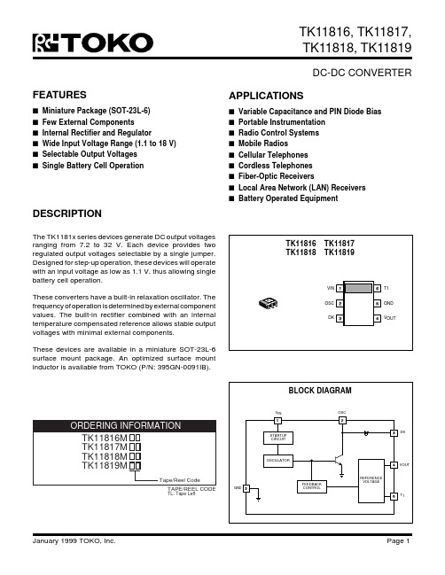
VIN
OSC
DK STARTUP CIRCUIT
OSCILLATOR
FEEDBACK CONTROL
REFERENCE VOLTAGE
VOUT T1
January 1999 TOKO, Inc.
Page 1
元器件交易网
TK11816, TK11817, TK11818, TK11819
0.3
UNITS mA mA V V mA mA %
mV/° C mV/° C
TK11819 ELECTRICAL CHARACTERISTICS
Test Conditions: VIN = 5 V, TA = 25 °C (Notes 3 & 5), unless otherwise specified.
TYP 4.7 12.1 16.8 9.30 4.5 6.0 0.06 1.81 2.31
MAX 9.0 19.0 17.6 9.80
0.3
UNITS mA mA V V mA mA %
mV/° C mV/° C
Page 2
January 1999 TOKO, Inc.
元器件交易网
SYMBOL
PARAMETER
TEST CONDITIONS
MIN
IIN
Supply Current
VOUT
Output Voltage
IOUT
Output Current
Load Reg Load Regulation
VOUT = 16.8 V, IOUT = 0.1 mA
VOUT = 9.3 V, IOUT = 1.0 mA
TK11816 TK11817 TK11818 TK11819
罗克韦尔 ControlLogix 系统 说明书
准备事宜 . . . . . . . . . . . . . . . . . . . . . . . . . . . . . . . . . . . . . . . . . . . . . . . . . . 19 1756-L7x 控制器部件. . . . . . . . . . . . . . . . . . . . . . . . . . . . . . . . . . . . . . 19
未随 1756-L6x 控制器提供的部件. . . . . . . . . . . . . . . . . . . . . . 33 1756-L6x 控制器安装. . . . . . . . . . . . . . . . . . . . . . . . . . . . . . . . . . . . . . 34 CF 卡的安装和取出 . . . . . . . . . . . . . . . . . . . . . . . . . . . . . . . . . . . . . . . 34 电池的连接与更换 . . . . . . . . . . . . . . . . . . . . . . . . . . . . . . . . . . . . . . . . 38 将控制器插入机架 . . . . . . . . . . . . . . . . . . . . . . . . . . . . . . . . . . . . . . . . 40 将控制器从机架拆下 . . . . . . . . . . . . . . . . . . . . . . . . . . . . . . . . . . . . . . 42
安装 1756-L7x 控制器 安装 1756-L6x 控制器
控制器使用入门
ADM1818中文资料

REV.0Information furnished by Analog Devices is believed to be accurate and reliable. However, no responsibility is assumed by Analog Devices for its use, nor for any infringements of patents or other rights of third parties which may result from its use. No license is granted by implication or otherwise under any patent or patent rights of Analog Devices.aADM1810–ADM1813/ADM1815–ADM1818One Technology Way, P.O. Box 9106, Norwood, MA 02062-9106, U.S.A.Tel: 781/329-4700World Wide Web Site: Fax: 781/326-8703© Analog Devices, Inc., 1999Microprocessor Reset CircuitsFUNCTIONAL BLOCK DIAGRAMSV CCGNDV CCGNDV CCGNDV CCGNDFEATURESReliable Low Cost Voltage Monitor with Reset Output Supports Monitoring of Supplies Within 5%, 10%, 15%and 20% ToleranceActive High and Low Push-Pull Output Choices (ADM1810, ADM1812, ADM1815 and ADM1817)Open Drain Output Choices (ADM1811, ADM1813,ADM1816 and ADM1818)Can Be Used with a Manual Push-Button to Generate a Reset (ADM1813, ADM1818)Initialize Microprocessor Systems with Added Safety APPLICATIONSMicroprocessor Systems Computers ControllersIntelligent Instruments Automotive SystemsGENERAL DESCRIPTIONThe ADM181x range of voltage monitoring circuits can be used in any application where an electronic system needs to be reset when a voltage increases above or below a predetermined value.Because of the “reset delay time” incorporated into the ADM181x series, these devices can provide a safe startup for electronic systems. Before a system initializes, the power supply must stabi-lize. Using the ADM181x series ensures that there are typically 150 ms for the power supply to stabilize before the system is reset and safe system initialization begins.The ADM181x series of microprocessor reset circuits are avail-able in low cost, space-saving SOT-23 packages.ADM1810–ADM1813/ADM1815–ADM1818–SPECIFICATIONS(T A = –40؇C to +85؇C unless otherwise noted)Parameter Min Typ Max Units Test Conditions/NoteSUPPLYVoltage 1.2 5.5VCurrent3040µA(ADM1810/ADM1811/ADM1813)V CC < 5.5 V, RST Output Open3040µA(ADM1812) V CC < 5.5 V2835µA(ADM1815/ADM1816/ADM1817/ADM1818)V CC < 5.5 V, RST Output OpenOUTPUT CURRENT8mA@ 0.4 V, V CC≥ 2.7 V*350µA(ADM1810/ADM1812/ADM1815/ADM1817)@ 2.4 V, V CC≥ 2.7 VOUTPUT VOLTAGE V CC – 0.5V CC – 0.1V(ADM1810/ADM1812/ADM1815/ADM1817)@ 0 µA to 500 µAV CC TRIP-POINTADM1810-5, ADM1810-10, ADM1810-15/ADM1811/ADM1812/ADM1813-5 4.50 4.62 4.75V(5%)ADM1811/ADM1812/ADM1813-10 4.25 4.35 4.49V(10%)ADM1811/ADM1812/ADM1813-15 4.00 4.13 4.24V(15%)ADM1815/ADM1816/ADM1817/ADM1818-5 2.98 3.06 3.15V(5%)ADM1815/ADM1816/ADM1817/ADM1818-10 2.80 2.88 2.97V(10%)ADM1815/ADM1816/ADM1817/ADM1818-20 2.47 2.55 2.64V(20%)INTERNAL PULL-UP RESISTORADM1811/ADM1813/ADM1816/ADM1818 3.5 5.57.5kΩOUTPUT CAPACITANCE10pFRESET ACTIVE TIME100150300msV CC DETECT TO RSTFalling510µs(ADM1810/ADM1811/ADM1812/ADM1813)715µs(ADM1815/ADM1816/ADM1817/ADM1818) Rising100150300ms t R = 5 µsPUSH-BUTTON DETECT TO RST1µs(ADM1813/ADM1818)PUSH-BUTTON RESET100150300ms(ADM1818) 2.7 V ≤ V CC≤ 3.3 V100150300ms(ADM1813)NOTES*For ADM181x-20, V CC = V CCTP, sink current reduces to 8 mA.Specifications subject to change without notice.REV. 0–2–REV. 0ADM1810–ADM1813/ADM1815–ADM1818–3–ORDERING GUIDENOTESRL7 or REEL7 are in reels of 3000 parts. REEL are in reels of 10000 parts.All models in bold are ex-stock. Consult factory for availability.*Only Available in Reels.ABSOLUTE MAXIMUM RATINGS*V CC . . . . . . . . . . . . . . . . . . . . . . . . . . . . . . . +1.2 V to +5.5 V Input Current . . . . . . . . . . . . . . . . . . . . . . . . . . . . . . . . 40 µA Operating Temperature Range . . . . . . . . . . . –40°C to +85°C Power Dissipation, RT-3, SOT-23 . . . . . . . . . . . . . . 320 mW Derate by 4 mW/°C Above +70°CθJA Thermal Impedance . . . . . . . . . . . . . . . . . . . . . . 333°C/W Lead Temperature (Soldering, 10 sec) . . . . . . . . . . . +300°C Vapor Phase (60 sec) . . . . . . . . . . . . . . . . . . . . . . . +215°C Infrared (15 sec) . . . . . . . . . . . . . . . . . . . . . . . . . . . +220°C Storage Temperature Range . . . . . . . . . . . . –65°C to +150°C ESD Rating . . . . . . . . . . . . . . . . . . . . . . . . . . . . . . . . . . .3 kV*Typical values are measured at T A = +25°C unless otherwise noted.PIN CONFIGURATIONV CC Figure 2.Power-Up Timing DiagramREV. 0ADM1810–ADM1813/ADM1815–ADM1818–4–C 3459–8–3/99P R I N T E D I N U .S .A .ADM1813 AND ADM1818The ADM1813 and ADM1818 are low cost voltage monitoring devices with the inclusion of an optional push-button reset function.Figure 3.ADM1813/ADM1818 Typical ApplicationAn optional push-button reset switch can be connected be-tween RST and ground. Pressing this switch will pull the reset output low. If the push-button reset button pulls the RST output low for a period greater than 1 µs, then, when the reset button releases the RST line to float high, the RST line will stay low for a further 150 ms typical.Figure 4.Push-Button Reset Timing DiagramThe ADM1818 range has options which allow the user to monitor 3.3 V supplies with 10% and 20% tolerance options.While the ADM1813 range has options which allow the user to monitor 5 V supplies with 5%, 10% and a 15% tolerance options.ADM1810, ADM1812, ADM1815 AND ADM1817The ADM1812 is a 5 V low cost voltage monitor with an active high push-pull output. The ADM1812 supports 5%, 10% and15% tolerances. The ADM1810 is similar to the ADM1812,except that the ADM1810 has an active low push-pull output.The ADM1817 is 3.3 V voltage monitor with an active high push-pull output. The ADM1817 supports 5%, 10% and 20%tolerances. The ADM1815 is similar to the ADM1817, except that the ADM1815 has an active low push-pull output.The ADM1810/ADM1812/ADM1815/ADM1817 can be con-nected directly to most microprocessor-reset inputs without the need for external components.Figure 5.ADM1810/ADM1812/ADM1815/ADM1817Typical ApplicationOUTLINE DIMENSIONSDimensions shown in inches and (mm).3-Lead Plastic Surface Mount Package (SOT-23)(RT-3)ADM1811 AND ADM1816The ADM1811 is a low cost voltage monitor with an open drain output. The ADM1811 is designed to monitor 5 V supplies.The ADM1811 range comes in three different variants which allow the monitoring of a 5 V supply with a tolerance of 5%,10% and 15%. The ADM1816 is a 3.3 V version of the ADM1811and supports 5%, 10% and 20% tolerance options.Figure 6.ADM1811/ADM1816 Typical Application。
TM1818

CLK-OUT tpLH1
----
80
延迟时间
LE-OUT tpLH2
VDD=5.0V
----
80
(低电平到高电平) OE-OUT tpLH3
VDS=1.0V
---- 115
CLK-SDO tpLH
VIH=Vdd
----
20
CLK-OUT tpLH1
VIL=GND
----
80
延迟时间
LE-OUT tpLH2
OUT15=OFF Rext=1860Ω, OUT0~
OUT15=ON Rext=744Ω, OUT0~
OUT15=ON
----3
--------0.8VD D GND
--------4.6 ---------
---------
-----
-----
250 250 -----
-----
-----
----
CLK-SDO tpLH
CLK-OUT
延迟时间
LE-OUT
(高电平到低电平) OE-OUT
CLK-SDO
电流输出上升沿时间
tpLH1 tpLH2 tpLH3 tpLH tor
电流输出下降沿时间
tof
十五、动态特性的测试电路
16 位恒流驱动 IC
VDS=1.0V VIH=Vdd
VIL=GND Rext=830Ω
Pull-up 电阻
RIN(up)
0E
250
500
800 KΩ
Pull-down 电阻
RIN(down)
LE
250
500
800 KΩ
IDD(off)1
Rext=未接, OUT0~ OUT15=OFF
- 1、下载文档前请自行甄别文档内容的完整性,平台不提供额外的编辑、内容补充、找答案等附加服务。
- 2、"仅部分预览"的文档,不可在线预览部分如存在完整性等问题,可反馈申请退款(可完整预览的文档不适用该条件!)。
- 3、如文档侵犯您的权益,请联系客服反馈,我们会尽快为您处理(人工客服工作时间:9:00-18:30)。
ห้องสมุดไป่ตู้
元器件交易网
Excelics
• • • • • • 18.15-18.75GHz BANDWIDTH AND INPUT/OUTPUT IMPEDANCE MATCHED TO 50 OHM EIA FEATURES HIGH PAE( 25% TYPICAL) EIB FEATURES HIGH IP3(43dBm TYPICAL) +30.0/+29.5dBm TYPICAL P1dB OUTPUT POWER FOR EIA/EIB 6.5/5.5dB TYPICAL G1dB POWER GAIN FOR EIA/EIB NON-HERMETIC METAL FLANGE PACKAGE
MAXIMUM RATINGS AT 25OC
SYMBOLS Vds Vgs Ids Igsf Pin Tch Tstg Pt PARAMETERS Drain-Source Voltage Gate-Source Voltage Drain Current Forward Gate Current Input Power Channel Temperature Storage Temperature Total Power Dissipation ABSOLUTE1 12V -8V Idss 90mA 32dBm 175oC -65/175oC 8.5W 8V -3V Idss 15mA @ 3dB Compression 150oC -65/150oC 7.1W CONTINUOUS2
EIA/EIB1818-1P
Not recommended for new designs. Contact factory. Effective 03/2003 18.15-18.75GHz, 1W Internally Matched Power FET
ELECTRICAL CHARACTERISTICS (Ta = 25 OC)
rd
EIB1818-1P MAX MIN 29.0 5.0 TYP 29.5 5.5 MAX UNIT dBm dB
MIN 29 6.0
TYP 30.0 6.5
P1dB G1dB PAE Id1dB IP3 Idss Gm Vp BVgd Rth
25 440 37 720 760 -1.0 -15 16 -2.5 850 550
Note: 1. Exceeding any of the above ratings may result in permanent damage. 2. Exceeding any of the above ratings may reduce MTTF below design goals.
Excelics Semiconductor, Inc., 310 De Guine Drive, Sunnyvale, CA 94085
20 425 43* 720 360 -2.0 -15 16
o
% mA dBm 850 mA mS -3.5 V V C/W
Drain Breakdown Voltage Igd=2.4mA Thermal Resistance (Au-Sn Eutectic Attach)
*Typical –45dBc IM3 at Pout=20dBm/Tone
EIA1818-1P SYMBOLS PARAMETERS/TEST CONDITIONS Output Power at 1dB Compression f=18.15-18.75GHz Vds=8V, Idsq=0.5 Idss(EIA), 0.6Idss(EIB) Gain at 1dB Compression f=18.15-18.75GHz Vds=8V, Idsq=0.5 Idss(EIA), 0.6Idss(EIB) Power Added Efficiency at 1dB compression f=18.15-18.75GHz Vds=8V, Idsq=0.5 Idss(EIA), 0.6Idss(EIB) Drain Current at 1dB Compression Output 3 Order Intercept Point f=18.15-18.75GHz Vds=8V, Idsq=0.5 Idss(EIA), 0.6Idss(EIB) Saturated Drain Current Vds=3V, Vgs=0V Transconductance Pinch-off Voltage Vds=3V, Vgs=0V Vds=3V, Ids=6mA -13 550