BD241C;BD241A;中文规格书,Datasheet资料
施耐德 TM241CE24R M241控制器内置以太网和串行通信端口 数据表

Product data sheetCharacteristicsTM241CE24RM241控制器内置以太网和串行通信端口主要信息产品系列Modicon M241产品类型可编程控制器额定电源电压 [Us]100...240 V 交流离散量输入数量14, 离散量输入 8 快速输入 符合 IEC 61131-2 类型 1固态输出类型继电器晶体管离散量输出数量 6 继电器4 晶体管 4 快速输出离散量输出电压5...125 V 直流 适用 继电器输出 5...250 V 交流 适用 继电器输出 24 V 直流 适用 晶体管输出离散量输出电流2 A 适用 继电器输出 (Q4 (9)0.1 A 适用 快速输出(PTO 模式) (TR0...TR3) 0.5 A 适用 晶体管输出 (TR0...TR3)补充信息离散量I/O编号24I/O 拓展模块数7 (本地 I/O 体系) 14 (远程 I/O 体系)电源电压范围85…264 V 电网频率50/60 Hz 离散量输入逻辑阱或源离散量输入电压24 V 离散量输入电压类型直流电压状态1担保>= 15 V 适用 输入电压状态0担保<= 5 V 适用 输入离散量输入电流5 MA 适用 输入输入阻抗 4.7 kOhm 适用 输入响应时间50 µs 开, I0...I13 端子 适用 输入可配置滤波时间 1 µs 适用 快速输入离散量输出逻辑正逻辑(源)输出电压限制125 V 直流 继电器输出 30 V 直流 晶体管输出 277 V AC 继电器输出Maximum output frequency1 KHz 适用 晶体管输出20 KHz 适用 快速输出(PWM 模式) 100 KHz 适用 快速输出 (PLS 模式)精度+/- 0.1 % 在…上 0.02…0.1 kHz 适用 快速输出 +/- 1 % 在…上 0.1…1 kHz 适用 快速输出T h e i n f o r m a t i o n p r o v i d e d i n t h i s d o c u m e n t a t i o n c o n t a i n s g e n e r a l d e s c r i p t i o n s a n d /o r t e c h n i c a l c h a r a c t e r i s t i c s o f t h e p e r f o r m a n c e o f t h e p r o d u c t s c o n t a i n e d h e r e i n .T h i s d o c u m e n t a t i o n i s n o t i n t e n d e d a s a s u b s t i t u t e f o r a n d i s n o t t o b e u s e d f o r d e t e r m i n i n g s u i t a b i l i t y o r r e l i a b i l i t y o f t h e s e p r o d u c t s f o r s p e c i f i c u s e r a p p l i c a t i o n s .I t i s t h e d u t y o f a n y s u c h u s e r o r i n t e g r a t o r t o p e r f o r m t h e a p p r o p r i a t e a n d c o m p l e t e r i s k a n a l y s i s , e v a l u a t i o n a n d t e s t i n g o f t h e p r o d u c t s w i t h r e s p e c t t o t h e r e l e v a n t s p e c i f i c a p p l i c a t i o n o r u s e t h e r e o f .N e i t h e r S c h n e i d e r E l e c t r i c I n d u s t r i e s S A S n o r a n y o f i t s a f f i l i a t e s o r s u b s i d i a r i e s s h a l l b e r e s p o n s i b l e o r l i a b l e f o r m i s u s e o f t h e i n f o r m a t i o n c o n t a i n e d h e r e i n .保护类型短路保护 适用 晶体管输出带自动复位的短路及过载保护 适用 晶体管输出逆相保护 适用 晶体管输出无保护 适用 继电器输出复位时间10 Ms 自动复位 输出12 S 自动复位 快速输出存储容量64 MB 适用 系统内存 RAM数据备份128 MB 内置闪存卡 适用 用户项目备份数据存储设备<= 16 GB SD卡 (可选)电池类型BR2033 锂电池不充电, 电池寿命: 4 年累计运行时间 2 年 在…上 25 °C1K指令的执行时间0.3 Ms 适用 事件和周期性任务0.7 Ms 适用 其他指示应用程序结构8个外部事件任务3循环主任务+1飞轮任务8 事项4循环主任务实时时钟有时钟误差<= 60 s/month 在…上 25 °C定位功能PTO 功能 4 通道 (定位频率: 100 kHz)计算输入数 4 快速输入 (高数计数模式) 在…上 200 kHz14 标准输入 在…上 1 kHz控制信号类型A/B 在…上 100 kHz 适用 快速输入 (高数计数模式)脉冲/方向 在…上 200 kHz 适用 快速输入 (高数计数模式)单相 在…上 200 kHz 适用 快速输入 (高数计数模式)集成连接类型非隔离的串行链接 串行 1 和 RJ45 连接器 和 RS232/RS485 界面非隔离的串行链接 串行 2 和 可拆卸螺旋接线端子 连接器 和 RS485 界面USB 端口 和 mini B USB 2.0 连接器Ethernet 和 RJ45 连接器电源(串行 1)串行链接供电: 5 V, <200 mA传输率 1.2...115.2 kbit/s (默认115.2 kbit/s ) 用于总线长度为… 15 m 适用 RS4851.2...115.2 kbit/s (默认115.2 kbit/s ) 用于总线长度为… 3 m 适用 RS232480 Mbit/s 用于总线长度为… 3 m 适用 USB10/100 Mbit/s 适用 以太网通讯协议非隔离的串行链接: 串口Modbus 协议 主/从Ethernet 端口10BASE-T/100BASE-TX - 1 端口 铜电缆通讯服务FDRDHCP 服务器 通过TM4以太网开关网络模块DHCP客户 嵌入式以太网端口SMS通知正在更新固件SNMP 客户/服务器编程NGVL监控IEC VAR ACCESSFTP 客户/服务器下载SQL 客户网络通讯协议TCP客户 I/0扫描仪以太网/IP源 I/O 扫描仪 嵌入式以太网端口以太网/IP目标,网络通讯协议TCP服务器和网络通讯服务器TCP 从动装置基于TCP/UDP库从控制器发送和接收电子邮件Web服务器(WebVisu & XWeb系统)OPC UA 服务器DNS客户本地信号指示 1 个LED (绿色) for PWR:1 个LED (绿色) for RUN:1 个LED (红色) for 模块错误 (ERR):1 个LED (红色) for I/O 错误(I/O):1 个LED (绿色) for 可访问 SD卡 (SD):1 个LED (红色) for BAT:1 个LED (绿色) for SL1:1 个LED (绿色) for SL2:1 个LED (红色) for TM4母线故障:每通道1 LED (绿色) for I/O 状态:1 个LED (绿色) for 以太网端口活动:电气连接可拆卸螺旋接线端子用于输入与输出 (5.08mm倾斜)可拆卸螺旋接线端子用于连接 24 V 直流电源 (5.08mm倾斜)Maximum cable distance between devices非屏蔽电缆: <50 m 适用 输入屏蔽电缆: <10 m 适用 快速输入非屏蔽电缆: <50 m 适用 输出屏蔽电缆: <3 m 适用 快速输出隔离供电与内部逻辑之间 在…上 500 V ACNon-insulated between supply and ground标识CE传感器电源24 V 直流 在…上 400 mA 由控制器供给浪涌耐受2 KV 电源线 (AC) 共模 符合 IEC 61000-4-52 KV 继电器输出 共模 符合 IEC 61000-4-51 KV 屏蔽电缆 共模 符合 IEC 61000-4-51 KV 电源线 (AC) 差模 符合 IEC 61000-4-51 KV 继电器输出 差模 符合 IEC 61000-4-51 KV 输入 共模 符合 IEC 61000-4-51 KV 晶体管输出 共模 符合 IEC 61000-4-5网页服务网络服务器最大连接数8 网络通讯协议服务器8 SoMachine protocol10 网络服务器4 FTP服务器16 以太网/IP 目标8 网络通讯协议客户从站数量64 以太网Modbus:16 Ethernet/IP:周期时间10 Ms 16 Ethernet/IP64 Ms 64 以太网Modbus安装方式顶帽类型TH35-15 导轨安装 符合 IEC 60715顶帽类型 TH35-7.5 导轨安装 符合 IEC 60715板或有固定套件的板高度90 Mm深度95 Mm宽度150 Mm净重0.53 Kg环境符合标准ANSI/ISA 12-12-01CSA C22.2 No 142CSA C22.2 No 213IEC 61131-2:2007船用规格(LR, ABS, DNV, GL)UL 508产品认证RCM[RETURN]cULus[RETURN]CE[RETURN]UKCA[RETURN]DNV-GL[RETURN]ABS[RETUR 抗静电放电8 KV 空气中 符合 IEC 61000-4-24 KV 接触 符合 IEC 61000-4-2抗电磁域10 V/M 80 MHz...1 GHz 符合 IEC 61000-4-33 V/M 1.4 GHz-2 GHz 符合 IEC 61000-4-31 V/M2 GHz...3 GHz 符合 IEC 61000-4-3抗瞬时脉冲能力2 KV 符合 IEC 61000-4-4 (电源线)2 KV 符合 IEC 61000-4-4 (继电器输出)1 KV 符合 IEC 61000-4-4 (Ethernet线)1 KV 符合 IEC 61000-4-4 (串行链接)1 KV 符合 IEC 61000-4-4 (输入)1 KV 符合 IEC 61000-4-4 (晶体管输出)传导干扰阻力10 V 0.15...80 MHz 符合 IEC 61000-4-63 V 0.1...80 MHz 符合 船用规格(LR, ABS, DNV, GL)10 V 标定频率 (2, 3, 4, 6.2, 8.2, 12.6, 16.5, 18.8, 22, 25 MHz) 符合 船用规格(LR, ABS, DNV, G 电磁辐射传导发射 - 测试等级: 120...69 dBµV/m QP ( 电源线) 在…上 10…150 kHz 符合 IEC 55011传导发射 - 测试等级: 63 dBμV/m QP ( 电源线) 在…上 1.5…30 MHz 符合 IEC 55011传导发射 - 测试等级: 79 dBμV/m QP/66 dBμV/m AV ( 电源线) 在…上 0.15…0.5 MHz 符合 IEC传导发射 - 测试等级: 73 dBμV/m QP/60 dBμV/m AV ( 电源线) 在…上 0.5…300 MHz 符合 IEC 5辐射发射 - 测试等级: 40 dBμV/m QP A类 ( 10 m) 在…上 30…230 MHz 符合 IEC 55011传导发射 - 测试等级: 79...63 dBμV/m QP ( 电源线) 在…上 150…1500 kHz 符合 IEC 55011辐射发射 - 测试等级: 47 dBμV/m QP A类 ( 10 m) 在…上 230…1000 MHz 符合 IEC 55011抗瞬时断电10 Ms环境温度-10…50 °C (垂直安装)-10…55 °C (垂直安装)贮存环境温度-25…70 °C相对湿度10…95 %, 无凝结 (操作中)10…95 %, 无凝结 (存储期间)IP 保护等级IP20 保护盖就位污染等级2工作海拔0...2000 m存储高度0…3000 M抗振动 3.5 mm 在…上 5…8.4 Hz 在…上 均匀导轨3 gn 在…上 8.4…150 Hz 在…上 均匀导轨3.5 mm 在…上 5…8.4 Hz 在…上 面板安装3 gn 在…上 8.4…150 Hz 在…上 面板安装抗冲击15 gn 适用 11 ms包装单位Unit Type of Package 1PCENumber of Units in Package 11Package 1 Height11.208 CmPackage 1 Width13.04 CmPackage 1 Length18.656 CmPackage 1 Weight760.0 GUnit Type of Package 2S03Number of Units in Package 28Package 2 Height30 CmPackage 2 Width30 CmPackage 2 Length40 CmPackage 2 Weight 6.97 KgUnit Type of Package 3P06Number of Units in Package 364Package 3 Height75.0 CmPackage 3 Width40.0 CmPackage 3 Length80.0 CmPackage 3 Weight66 Kg可持续性产品类型Green Premium 产品REACh法规REACh 声明欧盟ROHS指令主动合规性(超出欧盟 RoHS 法定范围的产品)无汞是中国 ROHS 管理办法中国 ROHS 声明RoHS 豁免信息是环境披露产品环境文件流通资料产品使用寿命终期信息WEEE该产品必须经特定废物回收处理后弃置于欧盟市场,绝不可丢弃于垃圾桶中。
SN74BCT241DW,SN74BCT241DWE4,SN74BCT241DWG4,SN74BCT241N,SN74BCT241NE4, 规格书,Datasheet 资料
Addendum-Page 1PACKAGING INFORMATIONOrderable Device Status(1)Package Type PackageDrawingPins Package QtyEco Plan(2)Lead/Ball Finish MSL Peak Temp (3)Samples (Requires Login)5962-9074301M2A ACTIVE LCCC FK 201TBD Call TI Call TI 5962-9074301MRA ACTIVE CDIP J 201TBD Call TI Call TI 5962-9074301MSA ACTIVE CFP W 201TBD Call TI Call TI SN74BCT241DBLE OBSOLETE SSOP DB 20TBDCall TICall TISN74BCT241DW ACTIVE SOIC DW 2025Green (RoHS & no Sb/Br)CU NIPDAU Level-1-260C-UNLIM SN74BCT241DWE4ACTIVE SOIC DW 2025Green (RoHS & no Sb/Br)CU NIPDAU Level-1-260C-UNLIM SN74BCT241DWG4ACTIVE SOIC DW 2025Green (RoHS & no Sb/Br)CU NIPDAU Level-1-260C-UNLIM SN74BCT241N ACTIVE PDIP N 2020Pb-Free (RoHS)CU NIPDAU N / A for Pkg Type SN74BCT241NE4ACTIVE PDIP N 2020Pb-Free (RoHS)CU NIPDAU N / A for Pkg Type SN74BCT241NSR ACTIVE SO NS 20Green (RoHS & no Sb/Br)CU NIPDAU Level-1-260C-UNLIM SN74BCT241NSRE4ACTIVE SO NS 20Green (RoHS & no Sb/Br)CU NIPDAU Level-1-260C-UNLIM SN74BCT241NSRG4ACTIVE SO NS 20Green (RoHS & no Sb/Br)CU NIPDAU Level-1-260C-UNLIM SNJ54BCT241FK ACTIVE LCCC FK 201TBD POST-PLATE N / A for Pkg TypeSNJ54BCT241J ACTIVE CDIP J 201TBD A42N / A for Pkg Type SNJ54BCT241WACTIVECFPW201TBDCall TIN / A for Pkg Type(1)The marketing status values are defined as follows:ACTIVE: Product device recommended for new designs.LIFEBUY: TI has announced that the device will be discontinued, and a lifetime-buy period is in effect.NRND: Not recommended for new designs. Device is in production to support existing customers, but TI does not recommend using this part in a new design.PREVIEW: Device has been announced but is not in production. Samples may or may not be available.OBSOLETE: TI has discontinued the production of the device.(2)Eco Plan - The planned eco-friendly classification: Pb-Free (RoHS), Pb-Free (RoHS Exempt), or Green (RoHS & no Sb/Br) - please check /productcontent for the latest availability information and additional product content details.TBD: The Pb-Free/Green conversion plan has not been defined.Pb-Free (RoHS): TI's terms "Lead-Free" or "Pb-Free" mean semiconductor products that are compatible with the current RoHS requirements for all 6 substances, including the requirement that lead not exceed 0.1% by weight in homogeneous materials. Where designed to be soldered at high temperatures, TI Pb-Free products are suitable for use in specified lead-free processes.芯天下--/Pb-Free (RoHS Exempt): This component has a RoHS exemption for either 1) lead-based flip-chip solder bumps used between the die and package, or 2) lead-based die adhesive used between the die and leadframe. The component is otherwise considered Pb-Free (RoHS compatible) as defined above.Green (RoHS & no Sb/Br): TI defines "Green" to mean Pb-Free (RoHS compatible), and free of Bromine (Br) and Antimony (Sb) based flame retardants (Br or Sb do not exceed 0.1% by weight in homogeneous material)(3) MSL, Peak Temp. -- The Moisture Sensitivity Level rating according to the JEDEC industry standard classifications, and peak solder temperature.Important Information and Disclaimer:The information provided on this page represents TI's knowledge and belief as of the date that it is provided. TI bases its knowledge and belief on information provided by third parties, and makes no representation or warranty as to the accuracy of such information. Efforts are underway to better integrate information from third parties. TI has taken and continues to take reasonable steps to provide representative and accurate information but may not have conducted destructive testing or chemical analysis on incoming materials and chemicals. TI and TI suppliers consider certain information to be proprietary, and thus CAS numbers and other limited information may not be available for release.In no event shall TI's liability arising out of such information exceed the total purchase price of the TI part(s) at issue in this document sold by TI to Customer on an annual basis.OTHER QUALIFIED VERSIONS OF SN54BCT241, SN74BCT241 :•Catalog: SN74BCT241•Military: SN54BCT241NOTE: Qualified Version Definitions:•Catalog - TI's standard catalog product•Military - QML certified for Military and Defense ApplicationsAddendum-Page 2芯天下--/TAPE AND REEL INFORMATION*All dimensions are nominalDevicePackage Type Package Drawing Pins SPQReel Diameter (mm)Reel Width W1(mm)A0(mm)B0(mm)K0(mm)P1(mm)W (mm)Pin1Quadrant SN74BCT241NSR SONS20330.024.48.213.02.512.024.0Q1*All dimensions are nominalDevice Package Type Package Drawing Pins SPQ Length(mm)Width(mm)Height(mm)SN74BCT241NSR SO NS200367.0367.045.0IMPORTANT NOTICETexas Instruments Incorporated and its subsidiaries(TI)reserve the right to make corrections,enhancements,improvements and other changes to its semiconductor products and services per JESD46C and to discontinue any product or service per JESD48B.Buyers should obtain the latest relevant information before placing orders and should verify that such information is current and complete.All semiconductor products(also referred to herein as“components”)are sold subject to TI’s terms and conditions of sale supplied at the time of order acknowledgment.TI warrants performance of its components to the specifications applicable at the time of sale,in accordance with the warranty in TI’s terms and conditions of sale of semiconductor products.Testing and other quality control techniques are used to the extent TI deems necessary to support this warranty.Except where mandated by applicable law,testing of all parameters of each component is not necessarily performed.TI assumes no liability for applications assistance or the design of Buyers’products.Buyers are responsible for their products and applications using TI components.To minimize the risks associated with Buyers’products and applications,Buyers should provide adequate design and operating safeguards.TI does not warrant or represent that any license,either express or implied,is granted under any patent right,copyright,mask work right,or other intellectual property right relating to any combination,machine,or process in which TI components or services are rmation published by TI regarding third-party products or services does not constitute a license to use such products or services or a warranty or endorsement e of such information may require a license from a third party under the patents or other intellectual property of the third party,or a license from TI under the patents or other intellectual property of TI.Reproduction of significant portions of TI information in TI data books or data sheets is permissible only if reproduction is without alteration and is accompanied by all associated warranties,conditions,limitations,and notices.TI is not responsible or liable for such altered rmation of third parties may be subject to additional restrictions.Resale of TI components or services with statements different from or beyond the parameters stated by TI for that component or service voids all express and any implied warranties for the associated TI component or service and is an unfair and deceptive business practice. TI is not responsible or liable for any such statements.Buyer acknowledges and agrees that it is solely responsible for compliance with all legal,regulatory and safety-related requirements concerning its products,and any use of TI components in its applications,notwithstanding any applications-related information or support that may be provided by TI.Buyer represents and agrees that it has all the necessary expertise to create and implement safeguards which anticipate dangerous consequences of failures,monitor failures and their consequences,lessen the likelihood of failures that might cause harm and take appropriate remedial actions.Buyer will fully indemnify TI and its representatives against any damages arising out of the use of any TI components in safety-critical applications.In some cases,TI components may be promoted specifically to facilitate safety-related applications.With such components,TI’s goal is to help enable customers to design and create their own end-product solutions that meet applicable functional safety standards and requirements.Nonetheless,such components are subject to these terms.No TI components are authorized for use in FDA Class III(or similar life-critical medical equipment)unless authorized officers of the parties have executed a special agreement specifically governing such use.Only those TI components which TI has specifically designated as military grade or“enhanced plastic”are designed and intended for use in military/aerospace applications or environments.Buyer acknowledges and agrees that any military or aerospace use of TI components which have not been so designated is solely at the Buyer's risk,and that Buyer is solely responsible for compliance with all legal and regulatory requirements in connection with such use.TI has specifically designated certain components which meet ISO/TS16949requirements,mainly for automotive ponents which have not been so designated are neither designed nor intended for automotive use;and TI will not be responsible for any failure of such components to meet such requirements.Products ApplicationsAudio /audio Automotive and Transportation /automotiveAmplifiers Communications and Telecom /communicationsData Converters Computers and Peripherals /computersDLP®Products Consumer Electronics /consumer-appsDSP Energy and Lighting /energyClocks and Timers /clocks Industrial /industrialInterface Medical /medicalLogic Security /securityPower Mgmt Space,Avionics and Defense /space-avionics-defense Microcontrollers Video and Imaging /videoRFID OMAP Mobile Processors /omap TI E2E Community Wireless Connectivity /wirelessconnectivityMailing Address:Texas Instruments,Post Office Box655303,Dallas,Texas75265Copyright©2012,Texas Instruments Incorporated。
ASO241R;CMD4825;D53TP50CH;ASO241;ASO242;中文规格书,Datasheet资料

PCB Mount
Panelays
I/O Modules
Solid State Relays t Solid State Control Relays t I/O Modules
DPA
1Amp
120/240 Vac 16-Pin DIP SCR AC Switch Output Zero Cross Turn-On
Crydom's DPA solid state relays are compact 16-pin DIP packages that are ideal for high density automated assembled printed circuit boards.
5 7 7 6 5 6 4 7 4 5 5 6 6 5 6 7 4 7 5
ASO ASPF CMX CX/CXE CX241 CTX DIP DO/DMO DPA D2W LC LR LS MP MPF SPF/PF SDV/SDI SPA UPD
PCB Mount
DPA4119 DPA6119
20-140 20-280
control of the techniques used throughout manufacturing. This department works closely with our design engineering group, establishes assembly processes, and oversees a comprehensive on-premises machine shop which fabricates our assembly fixtures. As the work progresses, Material and Production Control employ our advanced computer system, upgraded with our customized software to keep manufacturing operations humming. The computer system employs integral MRP and MSP capabilities to generate detailed scheduling and planning information. Ceramic Hybrid Manufacturing also is performed in-house. Crydom manufactures all metallized ceramic substrates used in our relays — a major factor in product performance and reliability, including direct bond copper substrates.
BD240中文资料

BD240, BD240A, BD240B, BD240C PNP SILICON POWER TRANSISTORS2JUNE 1973 - REVISED MARCH 1997P R O D U C T I N F O R M A T I O NNOTES:5.These parameters must be measured using pulse techniques, t p = 300 µs, duty cycle ≤ 2%.6.These parameters must be measured using voltage-sensing contacts, separate from the current carrying contacts.†Voltage and current values shown are nominal; exact values vary slightly with transistor parameters.electrical characteristics at 25°C case temperaturePARAMETER TEST CONDITIONSMIN TYPMAXUNITV (BR)CEOCollector-emitter breakdown voltageI C = -30 mA (see Note 5)I B = 0BD240BD240A BD240B BD240C -45-60-80-100VI CESCollector-emitter cut-off current V CE = -55 VV CE = -70 V V CE = -90 V V CE =-115 VV BE =0V BE =0V BE =0V BE =0BD240BD240A BD240B BD240C -0.2-0.2-0.2-0.2mA I CEO Collector cut-off current V CE = -30 V V CE = -60 V I B =0I B =0BD240/240A BD240B/240C-0.3-0.3mA I EBO Emitter cut-off current V EB = -5 V I C =0-1µA h FE Forward current transfer ratio V CE = -4 V V CE = -4 V I C =-0.2A I C = -1Α(see Notes 5 and 6)4015V CE(sat)Collector-emitter saturation voltage I B = -0.2 A I C = -1A (see Notes 5 and 6)-0.7V V BE Base-emitter voltageV CE = -4 V I C = -1 A (see Notes 5 and 6)-1.3Vh feSmall signal forward current transfer ratio V CE = -10 V I C =-0.2A f = 1 kHz 20|h fe |Small signal forward current transfer ratioV CE = -10 VI C =-0.2Af = 1 MHz3thermal characteristicsPARAMETERMINTYPMAX UNIT R θJC Junction to case thermal resistance 4.17°C/W R θJAJunction to free air thermal resistance62.5°C/Wresistive-load-switching characteristics at 25°C case temperaturePARAMETERTEST CONDITIONS †MIN TYP MAX UNIT t on T urn-on time I C = -200 mA V BE(off) = 3.4 VI B(on) = -20 mA R L = 150 ΩI B(off) = 20 mA t p = 20 µs, dc ≤ 2%0.2µs t offT urn-off time0.4µs3BD240, BD240A, BD240B, BD240C PNP SILICON POWER TRANSISTORS4JUNE 1973 - REVISED MARCH 1997P R O D U C T I N F O R M A T I O NMAXIMUM SAFE OPERATING REGIONSTHERMAL INFORMATION5BD240, BD240A, BD240B, BD240C PNP SILICON POWER TRANSISTORS6JUNE 1973 - REVISED MARCH 1997P R O D U C T I N F O R M A T I O NIMPORTANT NOTICEPower Innovations Limited (PI) reserves the right to make changes to its products or to discontinue any semiconductor product or service without notice, and advises its customers to verify, before placing orders, that the information being relied on is current.PI warrants performance of its semiconductor products to the specifications applicable at the time of sale in accordance with PI's standard warranty. Testing and other quality control techniques are utilized to the extent PI deems necessary to support this warranty. Specific testing of all parameters of each device is not necessarily performed, except as mandated by government requirements.PI accepts no liability for applications assistance, customer product design, software performance, or infringement of patents or services described herein. Nor is any license, either express or implied, granted under any patent right, copyright, design right, or other intellectual property right of PI covering or relating to any combination,machine, or process in which such semiconductor products or services might be or are used.PI SEMICONDUCTOR PRODUCTS ARE NOT DESIGNED, INTENDED, AUTHORIZED, OR WARRANTED TO BE SUIT ABLE FOR USE IN LIFE-SUPPORT APPLICA TIONS, DEVICES OR SYSTEMS.Copyright © 1997, Power Innovations Limited。
三极管代换大全

用万用表检测三极管时,第一次表盘有读数,第二次就没读数,是为什么?还有就是用hfe档位怎样检测三极管?回答:4 人气:14 提问时间:2009-10-25 21:15答案指针万用表测三极管好坏,极性:①测 NPN 三极管:将万用表欧姆挡置"R × 100" 或"R × lk" 处,把黑表笔接在基极上,将红表笔先后接在其余两个极上,如果两次测得的电阻值都较小,再将红表笔接在基极上,将黑表笔先后接在其余两个极上,如果两次测得的电阻值都很大,则说明三极管是好的。
②测 PNP 三极管:将万用表欧姆挡置"R × 100" 或"R × lk" 处,把红表笔接在基极上,将黑表笔先后接在其余两个极上,如果两次测得的电阻值都较小,再将黑表笔接在基极上,将红表笔先后接在其余两个极上,如果两次测得的电阻值都很大,则说明三极管是好的。
当三极管上标记不清楚时,可以用万用表来初步确定三极管的好坏及类型 (NPN 型还是 PNP型 ),并辨别出e、b、c三个电极。
测试方法如下 :①用指针式万用表判断基极 b 和三极管的类型:将万用表欧姆挡置"R × 100" 或"R×lk" 处,先假设三极管的某极为"基极",并把黑表笔接在假设的基极上,将红表笔先后接在其余两个极上,如果两次测得的电阻值都很小(或约为几百欧至几千欧 ),则假设的基极是正确的,且被测三极管为 NPN 型管;同上,如果两次测得的电阻值都很大( 约为几千欧至几十千欧 ), 则假设的基极是正确的,且被测三极管为 PNP 型管。
如果两次测得的电阻值是一大一小,则原来假设的基极是错误的,这时必须重新假设另一电极为"基极",再重复上述测试。
②判断集电极c和发射极e:仍将指针式万用表欧姆挡置"R × 100"或"R × 1k" 处,以NPN管为例,把黑表笔接在假设的集电极c上,红表笔接到假设的发射极e上,并用手捏住b和c极 ( 不能使b、c直接接触 ), 通过人体 , 相当 b 、 C 之间接入偏置电阻 , 读出表头所示的阻值 , 然后将两表笔反接重测。
健伍TM241A说明书
健伍TM-241A/441A中文操作说明由原版英文说明书翻译而得编译:马玉成2003年11月于大连目录1 使用前的注意事项 (4)2 规格参数 (6)3 随机附件 (7)4 安装 (8)5 操作控制部件及功能 (10)接收接收 (16)频率选择 (17)频率步长选择 (17)可编程频率方式(VFO)调谐限制 (18)ALT(仅对TM-541A/E有效) (19)发射 (20)超时定时器(TOT) (20)存储器后备电池 (21)初始状态 (21)初始化 (21)存储信道 (21)存储目录 (22)存储信道的存入 (22)存储信道的调出 (24)存储转移 (24)扫描扫描 (25)挂起/恢复 (25)频段扫描 (26)可编程频段扫描 (26)存储信道扫描 (27)存储信道跳过 (27)优先信道报警 (28)使用中继频差设定 (28)倒频功能 (29)亚音 (29)亚音频率选择 (29)自动补偿(仅对美国版有效) (30)连续单音静噪(CTCSS) (30)双音频静噪(DTSS) (31)数字录音(DRS) (34)分组 (41)音频报警 (47)自动关闭电源(APO) (48)屏幕背光(DIM) (48)提示音 (49)按键锁定 (49)6 电路图7 维修 (50)8 可选附件 (52)2 规格参数5 操作5-1-1 控制部件及功能①电源开关(POWER)接通或关闭电源。
按下VFO键或MR键同时接通电源将清除频率方式或存储信道的频率信息。
当电源接通时,手柄上的PF键可以编程。
②调谐旋钮选择发射或接收频率、存储信道、频率步长、亚音频率、扫描方向等。
③音量旋钮(VOL)调整扬声器的音量,顺时针方向转动将增大音量,逆时针方向转动减小音量。
④静噪旋钮(SQL)选择静噪阀值。
⑤功率/背光键(LOW/DIM)功率选择发射输出功率的大小(HI:高,MID:中,LOW:低)背光选择显示屏幕的背光亮度。
按住功能键(F)1秒钟以上,当F 显示闪烁时再按此键将开启或关闭超时定时器。
BD242C中文资料
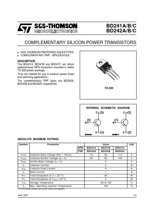
BD241A/B/C BD242A/B/CCOMPLEMENTARY SILICON POWER TRANSISTORSs SGS-THOMSON PREFERRED SALESTYPES sCOMPLEMENTARY PNP - NPN DEVICESDESCRIPTION The BD241A, BD241B and BD241C are silicon epitaxial-base NPN transistors mounted in Jedec TO-220 plastic package.They are inteded for use in medium power linear and switching applications.The complementary PNP types are BD242A,BD242B and BD242C respectively.June 1997ABSOLUTE MAXIMUM RATINGS1/4THERMAL DATAELECTRICAL CHARACTERISTICS (T case = 25 oC unless otherwise specified)For PNP types voltage and current values are negative.For the characteristics curves see TIP31/TIP32 series.BD241A/B/C/BD242A/B/C2/4BD241A/B/C/BD242A/B/C3/4Information furnished is believed to be accurate and reliable. However, SGS-THOMSON Microelectronics assumes no responsability for the consequences of use of such information nor for any infringement of patents or other rights of third parties which may results from its use. No license is granted by implication or otherwise under any patent or patent rights of SGS-THOMSON Microelectronics. Specifications mentioned in this publication are subject to change without notice. This publication supersedes and replaces all information previously supplied.SGS-THOMSON Microelectronics products are not authorized for use as critical components in life support devices or systems without express written approval of SGS-THOMSON Microelectonics.© 1997 SGS-THOMSON Microelectronics - Printed in Italy - All Rights ReservedSGS-THOMSON Microelectronics GROUP OF COMPANIESAustralia - Brazil - Canada - China - France - Germany - Hong Kong - Italy - Japan - Korea - Malaysia - Malta - Morocco - The Netherlands -Singapore - Spain - Sweden - Switzerland - Taiwan - Thailand - United Kingdom - U.S.A. . .BD241A/B/C/BD242A/B/C4/4。
电子技术专科教材013
2SC829
高频、低频放大
2SC62、2SC544、2SC561~562、2SCl686、2N3289~3292
3DGlllE
2SC911A
功放、振荡
2N5644
3DA816
2SC917
UHF高放、混频
2SC2466、2SC2728、2SC2731、2N6389
2DG302、FG024
四2输入与非门(OC)
四2输人或非门
四2输入与非门(OC)
六反相器
六反相器(OC)
六反相缓冲/驱动器(OC)
六缓冲/驱动器(OC)
四2输入与门
四2输入与门(OC)
三3输入与非门
三3输入与门
三3输入与非门(OC)
三3输入与门(OC)
六高压输出反相缓冲/驱动器(OC)
六高压输出缓冲/驱动器(OC)
双4辅人与非门
2SC920
高频放大、混频、变频
2SC33、2SC838~839,BF237~238
3DGlllF
2SC930
高频、小功率
2SC545、2SC772、2SC923、2N1992、2N3293~3294
3DG111D
2SCl008
高频、大电流
BCl41、BC301、BSSl5、BSS42、BSW39、2N5320
4线—七段译码器/驱动器(BCD输入,OC输出)
双2路2—2输入与或非门(一门可扩展)
双2路2—2(3)输入与或非门
4路2—3—2—2输人与或门(可扩展)
4路2—3—2—2输入与或非门(可扩展)
2路4—4输入与或非门(可扩展)
1/50分频器
双4输入与扩展器
- 1、下载文档前请自行甄别文档内容的完整性,平台不提供额外的编辑、内容补充、找答案等附加服务。
- 2、"仅部分预览"的文档,不可在线预览部分如存在完整性等问题,可反馈申请退款(可完整预览的文档不适用该条件!)。
- 3、如文档侵犯您的权益,请联系客服反馈,我们会尽快为您处理(人工客服工作时间:9:00-18:30)。
July 2007Rev 21/9BD241A BD241CNPN power transistorsFeatures■NPN transistorsApplications■Audio, general purpose switching and amplifier transistorsDescriptionThe devices are manufactured in Planar technology with “Base Island” layout. Theresulting transistor shows exceptional high gain performance coupled with very low saturation voltage. The PNP types are BD242A and BD242C.Table 1.Device summaryOrder codes Marking Package Packaging BD241A BD241CBD241A BD241CTO-220TO-220Tube TubeAbsolute maximum ratings BD241A BD241C2/91 Absolute maximum ratingsTable 2.Absolute maximum ratingsSymbol ParameterValueUnitBD241ABD241C V CER Collector-emitter voltage (R BE = 100Ω) 70115V V CEO Collector-emitter voltage (I B = 0) 60100V V EBO Emitter-base voltage (I C = 0) 5V I C Collector current3A I CM Collector peak current (t p < ms)5A I B Base current1A P TOT Total dissipation at T case = 25°C 40W T stg Storage temperature-65 to 150°C T JMax. operating junction temperature150°CBD241A BD241C Electrical characteristics3/92 Electrical characteristics(T case = 25°C; unless otherwise specified)2.1 Electrical characteristic (curves)Table 3.Electrical characteristicsSymbol ParameterTest Conditions Min.Typ.Max.Unit I CES Collector cut-off current (V BE = 0)V CE = rated V CEO0.2mA I CEO Collector cut-off current (I B = 0)for BD241A V CE =30V for BD241C V CE =60V 0.30.3mA mA I EBOEmitter cut-off current(I C = 0)V EB =5V 1mAV CEO(sus)(1)1.Pulsed duration = 300 ms, duty cycle ≥1.5%.Collector-emittersustaining voltage(I B = 0)I C =30mA for BD241A for BD241C 60100V V V CE(sat)(1)Collector-emitter saturation voltage I C =3A I B =0.6A 1.2V V BE (1)Base-emitter voltage I C =3A V CE =4V 1.8Vh FE (1)DC current gainI C =1A V CE =4V I C =3A V CE =4V2510Figure 2.Safe operating areaFigure 3.Derating curveElectrical characteristics BD241A BD241C4/9Figure 4.DC current gain Figure 5.DC current gainFigure 6.Collector-emitter saturationFigure 7.Base-emitter saturation Figure 8.Base-emitter on voltageFigure 9.Resistive load switching timeBD241A BD241CElectrical characteristics5/92.2 Test circuitsFigure 10.Resistive load switching timePackage mechanical data BD241A BD241C 3 Package mechanical dataIn order to meet environmental requirements, ST offers these devices in ECOPACK®packages. These packages have a Lead-free second level interconnect . The category ofsecond level interconnect is marked on the package and on the inner box label, in compliance with JEDEC Standard JESD97. The maximum ratings related to soldering conditions are also marked on the inner box label. ECOPACK is an ST trademark. ECOPACK specifications areavailable at: 6/9BD241A BD241C Package mechanical data7/9Revision history BD241A BD241C8/94 RevisionhistoryTable 4.Revision historyDate Revision Changes 01-Dec-20001Initial Release10-Jul-20072Figure 2 and figure 3, have been added.BD241A BD241CPlease Read Carefully:Information in this document is provided solely in connection with ST products. STMicroelectronics NV and its subsidiaries (“ST”) reserve the right to make changes, corrections, modifications or improvements, to this document, and the products and services described herein at any time, without notice.All ST products are sold pursuant to ST’s terms and conditions of sale.Purchasers are solely responsible for the choice, selection and use of the ST products and services described herein, and ST assumes no liability whatsoever relating to the choice, selection or use of the ST products and services described herein.No license, express or implied, by estoppel or otherwise, to any intellectual property rights is granted under this document. If any part of this document refers to any third party products or services it shall not be deemed a license grant by ST for the use of such third party products or services, or any intellectual property contained therein or considered as a warranty covering the use in any manner whatsoever of such third party products or services or any intellectual property contained therein.UNLESS OTHERWISE SET FORTH IN ST’S TERMS AND CONDITIONS OF SALE ST DISCLAIMS ANY EXPRESS OR IMPLIED WARRANTY WITH RESPECT TO THE USE AND/OR SALE OF ST PRODUCTS INCLUDING WITHOUT LIMITATION IMPLIED WARRANTIES OF MERCHANTABILITY, FITNESS FOR A PARTICULAR PURPOSE (AND THEIR EQUIVALENTS UNDER THE LAWS OF ANY JURISDICTION), OR INFRINGEMENT OF ANY PATENT, COPYRIGHT OR OTHER INTELLECTUAL PROPERTY RIGHT. UNLESS EXPRESSLY APPROVED IN WRITING BY AN AUTHORIZED ST REPRESENTATIVE, ST PRODUCTS ARE NOT RECOMMENDED, AUTHORIZED OR WARRANTED FOR USE IN MILITARY, AIR CRAFT, SPACE, LIFE SAVING, OR LIFE SUSTAINING APPLICATIONS, NOR IN PRODUCTS OR SYSTEMS WHERE FAILURE OR MALFUNCTION MAY RESULT IN PERSONAL INJURY, DEATH, OR SEVERE PROPERTY OR ENVIRONMENTAL DAMAGE. ST PRODUCTS WHICH ARE NOT SPECIFIED AS "AUTOMOTIVE GRADE" MAY ONLY BE USED IN AUTOMOTIVE APPLICATIONS AT USER’S OWN RISK.Resale of ST products with provisions different from the statements and/or technical features set forth in this document shall immediately void any warranty granted by ST for the ST product or service described herein and shall not create or extend in any manner whatsoever, any liability of ST.ST and the ST logo are trademarks or registered trademarks of ST in various countries.Information in this document supersedes and replaces all information previously supplied.The ST logo is a registered trademark of STMicroelectronics. All other names are the property of their respective owners.© 2007 STMicroelectronics - All rights reservedSTMicroelectronics group of companiesAustralia - Belgium - Brazil - Canada - China - Czech Republic - Finland - France - Germany - Hong Kong - India - Israel - Italy - Japan - Malaysia - Malta - Morocco - Singapore - Spain - Sweden - Switzerland - United Kingdom - United States of America9/9分销商库存信息:STMBD241C BD241A。