400384;中文规格书,Datasheet资料
NCV8450STT3G;中文规格书,Datasheet资料

NCV8450, NCV8450ASelf-Protected High Side Driver with Temperatureand Current LimitThe NCV8450/A is a fully protected High−Side Smart Discrete device with a typical R DS(on) of 1.0 W and an internal current limit of 0.8 A typical. The device can switch a wide variety of resistive, inductive, and capacitive loads.Features•Short Circuit Protection•Thermal Shutdown with Automatic Restart •Overvoltage Protection•Integrated Clamp for Inductive Switching•Loss of Ground Protection•ESD Protection•Slew Rate Control for Low EMI•Very Low Standby Current•NCV Prefix for Automotive and Other Applications Requiring Unique Site and Control Change Requirements; AEC−Q100 Qualified and PPAP Capable•This is a Pb−Free DeviceTypical Applications•Automotive•IndustrialPRODUCT SUMMARYSymbolCharacteristics Value Unit V IN_CL Overvoltage Protection54V V D(on)Operation Voltage 4.5 − 45V R on On−State Resistance 1.0WMARKINGDIAGRAM1AYWXXXXX GGXXXXX= V8450 or 8450AA= Assembly LocationY= YearW= Work WeekG= Pb−Free Package(Note: Microdot may be in either location)SOT−223(TO−261)CASE 318ESee detailed ordering and shipping information in the package dimensions section on page 8 of this data sheet.ORDERING INFORMATIONFigure 1. Block Diagram V (Pins 2, 4)OUT(Pin 3)IN(Pin 1)PACKAGE PIN DESCRIPTIONPin #Symbol Description1IN Control Input, Active Low2V D Supply Voltage3OUT Output4V D Supply VoltageMAXIMUM RATINGSRatingSymbol ValueUnit Min Max DC Supply Voltage (Note 1)V D −1645V Load Dump Protection(RI = 2 W , t d = 400 ms, V IN = 0, 10 V, I L = 150 mA, V bb = 13.5 V)V Loaddump100V Input CurrentIin −1515mAOutput Current (Note 1)I out Internally Limited A Total Power Dissipation@ T A = 25°C (Note 2)@ T A = 25°C (Note 3)P D1.131.60WElectrostatic Discharge (Note 4)(Human Body Model (HBM) 100 pF/1500 W )Input All other15kVSingle Pulse Inductive Load Switching Energy (Note 4)(V DD = 13.5 V, I = 465 mApk, L = 200 mH, T JStart = 150°C)E AS 29mJ Operating Junction Temperature T J −40+150°C Storage TemperatureT storage−55+150°CStresses exceeding Maximum Ratings may damage the device. Maximum Ratings are stress ratings only. Functional operation above the Recommended Operating Conditions is not implied. Extended exposure to stresses above the Recommended Operating Conditions may affect device reliability.1.Reverse Output current has to be limited by the load to stay within absolute maximum ratings and thermal performance.2.Minimum Pad.3. 1 in square pad size, FR −4, 1 oz Cu.4.Not subjected to production testing.THERMAL RESISTANCE RATINGSParameterSymbol Max Value Unit Thermal Resistance (Note 5)Junction −to −Ambient (Note 2)Junction −to −Ambient (Note 3)R q JA R q JA11078.3K/W5.Not subjected to production testing.Figure 2. Applications Test CircuitELECTRICAL CHARACTERISTICS (6 v V D v 45 V; −40°C <T J < 150°C unless otherwise specified)Rating Symbol ConditionsValueUnit Min Typ MaxOUTPUT CHARACTERISTICSOperating Supply Voltage V SUPPLY 4.5−45VOn Resistance(Pin 1 Connected to GND)R ON T J = 25°C , I OUT = 150 mA, V D = 7 V − 45 VT J = 150°C, I OUT = 150 mA, V D = 7 V − 45 V(Note 6)T J = 25°C , I OUT= 150 mA, V D = 6 V1.01.41.1232.1WStandby Current (Pin 1 Open)I D V D v 20 VV D> 20 V 0.610100m AINPUT CHARACTERISTICSInput Current – Off State I IN_OFF V OUT v 0.1 V, R L = 270 W, T J = 25°CV OUT v 0.1V, R L= 270 W, T J = 150°C (Note 6)−50−40m AInput Current – On State(Pin 1 Grounded)I IN_ON 1.53mA Input Resistance (Note 6)R IN1k W SWITCHING CHARACTERISTICSTurn−On Time (Note 7)(V IN = V D to 0 V) to 90% V OUT t ON R L = 270 W(Note 6)V D = 13.5 V, R L = 270 W, T J = 25°C30125100m sTurn−Off Time (Note 7)(V IN= 0 V to V D) to 10% V OUT t OFF R L = 270 W (Note 6)V D = 13.5 V, R L = 270 W, T J = 25°C60175150m sSlew Rate On (Note 7)(V IN = V D to 0V) 10% to 30% V OUT dV/dt ON R L = 270 W(Note 6)V D = 13.5 V, R L = 270 W, T J = 25°C0.744V/m sSlew Rate Off (Note 7)(V IN= 0 V to V D) 70% to 40% V OUT dV/dt OFF R L = 270 W (Note 6)V D = 13.5 V, R L = 270 W, T J = 25°C0.944V/m sOUTPUT DIODE CHARACTERISTICS (Note 6)Drain−Source Diode Voltage V F I OUT = −0.2 A0.6V Continuous Reverse DrainCurrentI S T J = 25°C0.2A PROTECTION FUNCTIONS (Note 8)Temperature Shutdown (Note 6)T SD150175−°C Temperature ShutdownHysteresis (Note 6)T SD_HYST5°COutput Current Limit I LIM T J = −40°C, V D = 13.5 V, t m = 100 m s (Note 6)T J = 25 °C, V D = 13.5 V, t m = 100 m sT J = 150 °C , V D = 13.5 V, t m = 100 m s (Note 6)0.50.81.5AOutput Clamp Voltage(Inductive Load Switch Off)At V OUT = V D− V CLAMPV CLAMP I OUT = 4 mA4552VOvervoltage Protection V IN_CL I CLAMP = 4 mA5054V6.Not subjected to production testing7.Only valid with high input slew rates8.Protection functions are not designed for continuous repetitive operation and are considered outside normal operating rangeR D S (o n ) (W )TEMPERATURE (°C)Figure 3. R DS(on) vs. TemperatureR D S (o n ) (W )OUTPUT LOAD (A)Figure 4. R DS(on) vs. Output LoadV D (V)Figure 5. R DS(on) vs. V DR D S (o n ) (W )1020304050607080T U R N O N T I M E (m s )TEMPERATURE (°C)Figure 6. Turn On Time vs. TemperatureTEMPERATURE (°C)Figure 7. Turn Off Time vs. TemperatureT U R N O F F T I M E (m s )S L E W R A T E (O N ) (V /m s )TEMPERATURE (°C)Figure 8. Slew Rate (ON) vs. Temperature−40−20020406080100120140−40−20020406080100120140−TEMPERATURE (°C)Figure 9. Slew Rate (OFF) vs. Temperature S L E W R A T E (O F F ) (V /m s )TEMPERATURE (°C)Figure 10. Current Limit vs. TemperatureC U R R E N T L I M I T (A )P E A K S C C U R R E N T (A )V D , VOLTAGE (V)Figure 11. Peak Short Circuit Current vs. V DVoltageTEMPERATURE (°C)Figure 12. V D Leakage Current vs.Temperature Off −StateV D , L E A K A G E C U R R E N T (m A )V D , L E A K A G E C U R R E N T (m A )V D , VOLTAGE (V)Figure 13. V D Leakage Current vs. V D VoltageOff −State TEMPERATURE (°C)Figure 14. On −State Input Current vs.TemperatureI N P U T C U R R E N T (m A )V D , VOLTAGE (V)Figure 15. Output Voltage vs. V D VoltageO U T P U T V O L T A G E (V )V D , VOLTAGE (V)Figure 16. Input Current vs. V D VoltageOn −StateI N P U T C U R R E N T (m A )LOAD INDUCTANCE (mH)Figure 17. Single Pulse Maximum Switch −offCurrent vs. Load InductanceC U R R E N T (m A )V D , VOLTAGE (V)Figure 18. Input Current vs. V D VoltageOff −StateI N P U T C U R R E N T (m A )−S H U T D O W N T I M E (m s )TEMPERATURE (°C)Figure 19. Initial Short −Circuit Shutdown Timevs. TemperaturePULSE TIME (s)R (t ), E F F E C T I V E T R A N S I E N T T H E R M AL R E S P O N S ECOPPER HEAT SPREADER AREA (mm 2)R q J A (°C /W )06080100120140Figure 20. R q JA vs. Copper Area2040Figure 21. Transient Thermal ResponseISO PULSE TEST RESULTSTest PulseTest Level Test ResultsPulse Cycle Time and Generator Impedance1200 V C 500 ms, 10 W 2150 V C 500 ms, 10 W 3a 200 V C 100 ms, 50 W 3b 200 V C 100 ms, 50 W 5175 VE(100 V)400 ms, 2 WORDERING INFORMATIONDevicePackage Shipping †NCV8450STT3G SOT −223(Pb −Free)4000 / Tape & Reel NCV8450ASTT3GSOT −223(Pb −Free)4000 / Tape & Reel†For information on tape and reel specifications, including part orientation and tape sizes, please refer to our Tape and Reel Packaging Specifications Brochure, BRD8011/D.PACKAGE DIMENSIONSSOT −223 (TO −261)CASE 318E −04ISSUE MNOTES:1.DIMENSIONING AND TOLERANCING PER ANSI Y14.5M, 1982.2.CONTROLLING DIMENSION: INCH.DIM A MIN NOM MAX MIN MILLIMETERS1.50 1.63 1.750.060INCHESA10.020.060.100.001b 0.600.750.890.024b1 2.90 3.06 3.200.115c 0.240.290.350.009D 6.30 6.50 6.700.249E 3.30 3.50 3.700.130e 2.20 2.30 2.400.0870.850.94 1.050.0330.0640.0680.0020.0040.0300.0350.1210.1260.0120.0140.2560.2630.1380.1450.0910.0940.0370.041NOM MAX L1 1.50 1.75 2.000.0606.707.007.300.2640.0690.0780.2760.287H E−−e10°10°0°10°q*For additional information on our Pb −Free strategy and solderingdetails, please download the ON Semiconductor Soldering and Mounting Techniques Reference Manual, SOLDERRM/D.SOLDERING FOOTPRINT*ON Semiconductor and are registered trademarks of Semiconductor Components Industries, LLC (SCILLC). SCILLC reserves the right to make changes without further notice to any products herein. SCILLC makes no warranty, representation or guarantee regarding the suitability of its products for any particular purpose, nor does SCILLC assume any liability arising out of the application or use of any product or circuit, and specifically disclaims any and all liability, including without limitation special, consequential or incidental damages.“Typical” parameters which may be provided in SCILLC data sheets and/or specifications can and do vary in different applications and actual performance may vary over time. All operating parameters, including “Typicals” must be validated for each customer application by customer’s technical experts. SCILLC does not convey any license under its patent rights nor the rights of others. SCILLC products are not designed, intended, or authorized for use as components in systems intended for surgical implant into the body, or other applications intended to support or sustain life, or for any other application in which the failure of the SCILLC product could create a situation where personal injury or death may occur. Should Buyer purchase or use SCILLC products for any such unintended or unauthorized application, Buyer shall indemnify and hold SCILLC and its officers, employees, subsidiaries, affiliates,and distributors harmless against all claims, costs, damages, and expenses, and reasonable attorney fees arising out of, directly or indirectly, any claim of personal injury or death associated with such unintended or unauthorized use, even if such claim alleges that SCILLC was negligent regarding the design or manufacture of the part. SCILLC is an Equal Opportunity/Affirmative Action Employer. This literature is subject to all applicable copyright laws and is not for resale in any manner.PUBLICATION ORDERING INFORMATION分销商库存信息: ONSEMINCV8450STT3G。
PE-68283NL;PE-68279NL;PE-68283NLT;中文规格书,Datasheet资料

Pulse Europe Einsteinstrasse 1 D-71083 Herrenberg Germany
Tel: 858 674 8100 Fax: 858 674 8262
Tel: 49 7032 7806 0 Fax: 49 7032 7806 12
Pulse China Headquarters B402, Shenzhen Tech-Innovation International Tenth Kejinan Rd. High-Tech Industrial Park Nanshan District, Shenzhen China Tel: 86 755 33966678 Fax: 86 755 33966700
NOTE: Add suffix "T" to part number for Tape & Reel package (i.e. PE-68279T).
80 mA /200 mA 80 mA /200 mA
±5% ±5%
1500 Vrms 1500 Vrms
Mechanical
Schematic
1.535,907MAX 11 10 9 8
12
7
.100 2,54
.190 4,83 .380 9,65
.300 7,62
.150 3,81
.050 1,27
.100 2,54 .200
5,08
13
PE-682XXNL
DATE CODE
6 1.14,5531MAX
C4
.050 1,27
.060 1,52
P599.B (10/07)
/
分销商库存信息:
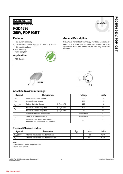
FGD4536TM;中文规格书,Datasheet资料
I CES Collector Cut-Off Current V CE = V CES, V GE = 0V--100µA I GES G-E Leakage Current V GE = V GES, V CE = 0V --±400nAOn CharacteristicsV GE(th)G-E Threshold Voltage I C = 250µA, V CE = V GE 2.4 3.3 4.0VV CE(sat)Collector to EmitterSaturation Voltage I C = 20A, V GE = 15V- 1.19-V I C = 30A, V GE = 15V- 1.33-V I C = 50A, V GE = 15V,T C = 25o C- 1.59 1.8V I C = 50A, V GE = 15V,T C = 125o C- 1.66-VDynamic CharacteristicsC ies Input CapacitanceV CE = 30V, V GE = 0V,f = 1MHz -1295-pFC oes Output Capacitance-56-pF C res Reverse Transfer Capacitance-43-pFSwitching Characteristicst d(on)Turn-On Delay TimeV CC = 200V, I C = 20A,R G = 5Ω, V GE = 15V,Resistive L oad, T C = 25o C -5-nst r Rise Time-20-ns t d(off)Turn-Off Delay Time-41-ns t f Fall Time-182-nst d(on)Turn-On Delay TimeV CC = 200V, I C = 20A,R G = 5Ω, V GE = 15V,Resistive Load, T C = 125o C -5-nst r Rise Time-21-ns t d(off)Turn-Off Delay Time-43-ns t f Fall Time-249-nsQ g Total Gate ChargeV CE = 200V, I C = 20A,V GE = 15V -47-nCQ ge Gate to Emitter Charge- 5.4-nC Q gc Gate to Collector Charge-15-nCDimensions in Millimeters*Trademarks of System General Corporation, used under license by Fairchild Semiconductor.DISCLAIMERFAIRCHILD SEMICONDUCTOR RESERVES THE RIGHT TO MAKE CHANGES WITHOUT FURTHER NOTICE TO ANY PRODUCTS HEREIN TO IMPROVE RELIABILITY, FUNCTION, OR DESIGN. FAIRCHILD DOES NOT ASSUME ANY LIABILITY ARISING OUT OF THE APPLICATION OR USE OF ANY PRODUCT OR CIRCUIT DESCRIBED HEREIN; NEITHER DOES IT CONVEY ANY LICENSE UNDER ITS PATENT RIGHTS, NOR THE RIGHTS OF OTHERS.THESE SPECIFICATIONS DO NOT EXPAND THE TERMS OF FAIRCHILD’S WORLDWIDE TERMS AND CONDITIONS, SPECIFICALLY THE WARRANTY THEREIN, WHICH COVERS THESE PRODUCTS.LIFE SUPPORT POLICYFAIRCHILD’S PRODUCTS ARE NOT AUTHORIZED FOR USE AS CRITICAL COMPONENTS IN LIFE SUPPORT DEVICES OR SYSTEMS WITHOUT THE EXPRESS WRITTEN APPROVAL OF FAIRCHILD SEMICONDUCTOR CORPORATION.As used here in:1. Life support devices or systems are devices or systems which, (a) areintended for surgical implant into the body or (b) support or sustain life,and (c) whose failure to perform when properly used in accordance with instructions for use provided in the labeling, can be reasonably expected to result in a significant injury of the user.2.A critical component in any component of a life support, device, or system whose failure to perform can be reasonably expected to cause the failure of the life support device or system, or to affect its safety or effectiveness.PRODUCT STATUS DEFINITIONS Definition of TermsDEUXPEED ®Dual Cool™EcoSPARK ®EfficentMax™ESBC™Fairchild ®Fairchild Semiconductor ®FACT Quiet Series™FACT®FAST ®FastvCore™FETBench™FlashWriter ® *FPS™ISOPLANAR™MegaBuck™MICROCOUPLER™MicroFET™MicroPak™MicroPak2™MillerDrive™MotionMax™Motion-SPM™OptiHiT™OPTOLOGIC ®OPTOPLANAR ®®PDP SPM™Power-SPM™Saving our world, 1mW/W/kW at a time™SignalWise™SmartMax™SMART START™SPM ®STEALTH™SuperFET ®SuperSOT™-3SuperSOT™-6SuperSOT™-8SupreMOS ®SyncFET™Sync-Lock™ ®*TINYOPTO™TinyPower™TinyPWM™TinyWire™TriFault Detect™TRUECURRENT™*µSerDes™UHC ®Ultra FRFET™UniFET™VCX™VisualMax™XS™®Datasheet Identification Product Status DefinitionAdvance Information Formative / In Design Datasheet contains the design specifications for product development. Specifications ANTI-COUNTERFEITING POLICYFairchild Semiconductor Corporation’s Anti-Counterfeiting Policy. Fairchild’s Anti-Counterfeiting Policy is also stated on our external website,, under Sales Support .Counterfeiting of semiconductor parts is a growing problem in the industry. All manufactures of semiconductor products are experiencing counterfeiting of their parts. Customers who inadvertently purchase counterfeit parts experience many problems such as loss of brand reputation, substandard performance, failed application, and increased cost of production and manufacturing delays. Fairchild is taking strong measures to protect ourselves and our customers from the proliferation of counterfeit parts. Fairchild strongly encourages customers to purchase Fairchild parts either directly from Fairchild or from Authorized Fairchild Distributors who are listed by country on our web page cited above. Products customers buy either from Fairchild directly or from Authorized Fairchild Distributors are genuine parts, have full traceability, meet Fairchild’s quality standards for handing and storage and provide access to Fairchild’s full range of up-to-date technical and product information. Fairchild and our Authorized Distributors will stand behind all warranties and will appropriately address and warranty issues that may arise. Fairchild will not provide any warranty coverage or other assistance for parts bought from Unauthorized Sources. Fairchild is committed to combat this global problem and encourage our customers to do their part in stopping this practice by buying direct or from authorized distributors.分销商库存信息: FAIRCHILDFGD4536TM。
DB3;DB4;SMDB3;中文规格书,Datasheet资料

October2001-Ed:2B DIACSymbol Parameter Value Unit I TRM Repetitive peak on-state currenttp=20µs F=120HzSMDB3 1.00ADB3/DB4 2.00Tstg Tj Storage temperature rangeOperating junction temperature range-40to+125°CABSOLUTE MAXIMUM RATINGS(limiting values)Note:*SMDB3indicated as Preliminary spec as product is still in development stage.1/55/5Information furnished is believed to be accurate and reliable.However,STMicroelectronics assumes no responsibility for the consequences of use of such information nor for any infringement of patents or other rights of third parties which may result from its use.No license is granted by implication or otherwise under any patent or patent rights of STMicroelectronics.Specifications mentioned in this publication are subject to change without notice.This publication supersedes and replaces all information previously supplied.STMicroelectronics products are not authorized for use as critical components in life support devices or systems without express written ap-proval of STMicroelectronics.The ST logo is a registered trademark of STMicroelectronics ©2001STMicroelectronics -Printed in Italy -All rights reserved.STMicroelectronics GROUP OF COMPANIESAustralia -Brazil -China -Finland -France -Germany -Hong Kong -India -Italy -Japan -MalaysiaMalta -Morocco -Singapore -Spain -Sweden -Switzerland -United Kingdom -U.S.A.PACKAGE MECHANICAL DATA (in millimeters)SOT-23FOOTPRINT分销商库存信息:STMDB3DB4SMDB3。
7448640412;中文规格书,Datasheet资料

description :Gehäuse / case: UTA 21,2 max mmB 16,6 max mmC 22,5 max mmD 13,0 ± 0,2mmE 10,0 ± 0,2mmF 4,5 max mm ø0,8 typmmEigenschaften /propertiesWert / valueEinheit / unittol.Leerlauf-Induktivität /inductanceDC-Widerstand /DC-resistance Nennstrom /rated current Nennspannung /rated voltage33%20 °C2000 V,50 HzHasAVersion 211-09-01MST Version 109-08-06NameÄnderung / modificationDatum / dateWAYNE KERR WK3260B/WK3265 für/for L 0 und/and R DC Klimabeständigkeit/ climatic class: 40/125/21 Datum / date............................................................................. A Mechanische Abmessungen / dimensions :10 kHz / 100 mV / 20°C B Elektrische Eigenschaften / electrical properties:25050 HzmHR DC VCURRENT-COMPENSATED CHOKE WE-FCKern / coreP155 IEC317-20Betriebstemp. / operating temperature: -25°C - + 125°C Übertemperatur / temperature rise: < 55 K L O 3,90 D Prüfgeräte / test equipment:E Testbedingungen / test conditions:@ 20 °C@ 70 °CDATUM / DATE : 2011-09-01±15%A Testbedingungen / test conditions 1,000,27minC Schaltbild / schematic:Unterschrift / signature Kontrolliert / approvedWürth Elektronik eiSos GmbH & Co. KGD-74638 Waldenburg · Max-Eyth-Strasse 1 - 3 · Germany · Telefon (+49) (0) 7942 - 945 - 0 · Telefax (+49) (0) 7942 - 945 - 400Geprüft / checked ..........................................................................................................................................Prüfspannung / isolation voltageU NI N Luftfeuchtigkeit / humidity:HP 34401 A für/for INUmgebungstemperatur / temperature:Würth Elektronik..................................................................................G Eigenschaften / general specifications:Gehäuse / case:Freigabe erteilt / general release:Kunde / customerDraht / wire:UL94V-0 F Werkstoffe & Zulassungen / material & approvals:MnZn-Ferrite / MnZn ferriteIt is recommended that the temperature of the part does not exceed 125°C under worst case operating conditions.This electronic component has been designed and developed for usage in general electronic equipment. Before incorporating thi s component into any equipment where higher safety and reliability isespecially required or if there is the possibility of direct damage or injury to human body, for example in the range of aero space, aviation, nuclear control, submarine, transportation, (automotive control, train control, ship control), transportation signal, disaster prevention, medical, public information network etc, Würth Elektronik eiSos GmbH must be informed before the design-in stage. In addition, sufficient reliability evaluation checks for safety must be performed on every electronic component which is used in electrical circuits that require high safety and reliability functions or performance.1 2N134N21 2 34HasAVersion 211-09-01MST Version 109-08-06NameÄnderung / modificationDatum / dateGeprüft / checked Kontrolliert / approvedWürth Elektronik eiSos GmbH & Co. KGD-74638 Waldenburg · Max-Eyth-Strasse 1 - 3 · Germany · Telefon (+49) (0) 7942 - 945 - 0 · Telefax (+49) (0) 7942 - 945 - 400H Einfügungsdämpfung / insertion loss:Geprüft / checkedKontrolliert / approvedDatum / date ..................................................................................= = = = =common modeThis electronic component has been designed and developed for usage in general electronic equipment. Before incorporating thi s component into any equipment where higher safety and reliability is especially required or if there is the possibility of direct damage or injury to human body, for example in the range of aero space, aviation, nuclear control, submarine, transportation, (automotive control, train control, ship control), transportation signal, disaster prevention, medical, public information network etc, W ürth Elektronik eiSos GmbH must be informed before the design -in stage. In addition, sufficient reliability evaluation checks for safety must be performed on every electronic component which is used i n electrical circuits that require high safety and reliability functions or performance.Bezeichnung :description :..................................................................................HasAVersion 211-09-01..................................................................................MSTVersion 109-08-06Name Änderung / modificationDatum / dateKunde / customer..................................................................................Geprüft / checkedSTROMKOMPENSIERTE DROSSEL WE-FC Datum / dateKontrolliert / approvedD-74638 Waldenburg · Max-Eyth-Strasse 1 - 3 · Germany · Telefon (+49) (0) 7942 - 945 - 0 · Telefax (+49) (0) 7942 - 945 - 400Würth Elektronik eiSos GmbH & Co. KGUnterschrift / signature Würth ElektronikFreigabe erteilt / general release:CURRENT-COMPENSATED CHOKE WE-FC..................................................................DATUM / DATE : 2011-09-01I Stangenspezifikation / tube specification:This electronic component has been designed and developed for usage in general electronic equipment. Before incorporating thi s component into any equipment where higher safety and reliability is especially required or if there is the possibility of direct damage or injury to human body, for example in the range of aero space, aviation, nuclear control, submarine, transportation, (automotive control, train control, ship control), transportation signal, disaster prevention, medical, public information network etc, W ürth Elektronik eiSos GmbH must be informed before the design -in stage. In addition, sufficient reliability evaluation checks for safety must be performed on every electronic component which is used i n electrical circuits that require high safety and reliability functions or performance.分销商库存信息: WURTH-ELECTRONICS 7448640412。
TPCF8304(TE85L,F);中文规格书,Datasheet资料

Drain power
(Note 3a)
dissipation
(t = 5 s) (Note 2b) Single-device value at
dual operation (Note 3b)
Single-pulse avalanche energy (Note 4)
Avalanche current
TPCF8304
TOSHIBA Field Effect Transistor Silicon P-Channel MOS Type (U-MOS IV)
TPCF8304
Notebook PC Applications Portable Equipment Applications
Unit: mm
• Low drain-source ON resistance: RDS (ON) = 60 mΩ (typ.) • High forward transfer admittance: |Yfs| = 5.9 S (typ.) • Low leakage current: IDSS = −10 μA (max) (VDS = −30 V) • Enhancement model: Vth = −0.8 to −2.0 V (VDS = −10 V, ID = −1 mA)
Note 4: VDD = -24 V, Tch = 25°C (initial), L = 0.2 mH, RG = 25 Ω, IAR = -1.6 A Note 5: Repetitive rating; pulse width limited by max channel stemperature
Switching time
Turn-on time Fall time
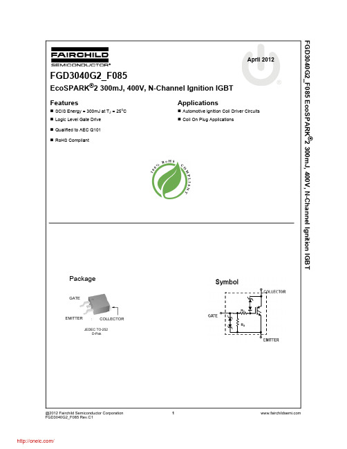
FGD3040G2;中文规格书,Datasheet资料
2
FGD3040G2_F085 Rev.C1
/
FGD3040G2_F085 EcoSPARK®2 300mJ, 400V, N-Channel Ignition IGBT
Electrical Characteristics TA = 25°C unless otherwise noted
FGD3040G2 FGD3040G2_F085
Package TO252
Reel Size 330mm
Ratings 400 28 300 170 41 25.6 ±10 150 1
-55 to +175 -55 to +175
300 260
4 2
Units V V mJ mJ A A V W
W/oC oC oC
Symbol
Parameter
Test Conditions
Min Typ Max Units
Dynamic Characteristics
QG(ON) Gate Charge VGE(TH) Gate to Emitter Threshold Voltage VGEP Gate to Emitter Plateau Voltage
390 420 450 V
28 -
-
V
±12 ±14 -
V
-
- 25 μA
-
-
1 mA
-
-
1
mA
-
- 40
- 120 - Ω
10K - 30K Ω
- 1.15 1.25 V - 1.35 1.50 V - 1.68 1.85 V
-
- 300 mJ
@2012 Fairchild Semiconductor Corporation
SN74LS138NSRG4;中文规格书,Datasheet资料

PACKAG PACKAGING INFORMATIONOrderable Device Status (1)Package Type PackageDrawing Pins Package Qty Eco Plan (2)Lead/Ball FinishMSL Pea76005012A ACTIVE LCCC FK201TBD Call TI Call TI7600501EA ACTIVE CDIP J161TBD Call TI Call TI7600501EA ACTIVE CDIP J161TBD Call TI Call TI7600501FA ACTIVE CFP W161TBD Call TI Call TI7600501FA ACTIVE CFP W161TBD Call TI Call TI76041012A ACTIVE LCCC FK201TBD Call TI Call TI76041012A ACTIVE LCCC FK201TBD Call TI Call TI7604101EA ACTIVE CDIP J161TBD Call TI Call TI7604101EA ACTIVE CDIP J161TBD Call TI Call TI7604101FA ACTIVE CFP W161TBD Call TI Call TI7604101FA ACTIVE CFP W161TBD Call TI Call TI JM38510/07701BEA ACTIVE CDIP J161TBD A42N / A for PkgJM38510/07701BEA ACTIVE CDIP J161TBD A42N / A for PkgJM38510/07701BFA ACTIVE CFP W161TBD A42N / A for PkgJM38510/07701BFA ACTIVE CFP W161TBD A42N / A for PkgJM38510/30701B2A ACTIVE LCCC FK201TBD POST-PLATE N / A for PkgJM38510/30701B2A ACTIVE LCCC FK201TBD POST-PLATE N / A for PkgJM38510/30701BEA ACTIVE CDIP J161TBD A42N / A for PkgJM38510/30701BEA ACTIVE CDIP J161TBD A42N / A for PkgJM38510/30701BFA ACTIVE CFP W161TBD A42N / A for PkgJM38510/30701BFA ACTIVE CFP W161TBD A42N / A for PkgJM38510/30701SEA ACTIVE CDIP J1625TBD A42N / A for PkgJM38510/30701SEA ACTIVE CDIP J1625TBD A42N / A for PkgJM38510/30701SFA ACTIVE CFP W1625TBD A42N / A for PkgJM38510/30701SFA ACTIVE CFP W1625TBD A42N / A for PkgM38510/07701BEA ACTIVE CDIP J161TBD A42N / A for PkgM38510/07701BEA ACTIVE CDIP J161TBD A42N / A for PkgM38510/07701BFA ACTIVE CFP W161TBD A42N / A for PkgM38510/07701BFA ACTIVE CFP W161TBD A42N / A for PkgM38510/30701B2A ACTIVE LCCC FK201TBD POST-PLATE N / A for Pkg /PACKAG Orderable Device Status (1)Package Type PackageDrawing Pins Package Qty Eco Plan (2)Lead/Ball FinishMSL PeaM38510/30701B2A ACTIVE LCCC FK201TBD POST-PLATE N / A for Pkg M38510/30701BEA ACTIVE CDIP J161TBD A42N / A for Pkg M38510/30701BEA ACTIVE CDIP J161TBD A42N / A for Pkg M38510/30701BFA ACTIVE CFP W161TBD A42N / A for Pkg M38510/30701BFA ACTIVE CFP W161TBD A42N / A for Pkg M38510/30701SEA ACTIVE CDIP J1625TBD A42N / A for Pkg M38510/30701SEA ACTIVE CDIP J1625TBD A42N / A for Pkg M38510/30701SFA ACTIVE CFP W1625TBD A42N / A for Pkg M38510/30701SFA ACTIVE CFP W1625TBD A42N / A for Pkg SN54LS138J ACTIVE CDIP J161TBD A42N / A for Pkg SN54LS138J ACTIVE CDIP J161TBD A42N / A for Pkg SN54S138J ACTIVE CDIP J161TBD A42N / A for Pkg SN54S138J ACTIVE CDIP J161TBD A42N / A for Pkg SN74LS138D ACTIVE SOIC D1640Green (RoHS& no Sb/Br)CU NIPDAU Level-1-260CSN74LS138D ACTIVE SOIC D1640Green (RoHS& no Sb/Br)CU NIPDAU Level-1-260CSN74LS138DE4ACTIVE SOIC D1640Green (RoHS& no Sb/Br)CU NIPDAU Level-1-260CSN74LS138DE4ACTIVE SOIC D1640Green (RoHS& no Sb/Br)CU NIPDAU Level-1-260CSN74LS138DG4ACTIVE SOIC D1640Green (RoHS& no Sb/Br)CU NIPDAU Level-1-260CSN74LS138DG4ACTIVE SOIC D1640Green (RoHS& no Sb/Br)CU NIPDAU Level-1-260CSN74LS138DR ACTIVE SOIC D162500Green (RoHS& no Sb/Br)CU NIPDAU Level-1-260CSN74LS138DR ACTIVE SOIC D162500Green (RoHS& no Sb/Br)CU NIPDAU Level-1-260CSN74LS138DRE4ACTIVE SOIC D162500Green (RoHS& no Sb/Br)CU NIPDAU Level-1-260CSN74LS138DRE4ACTIVE SOIC D162500Green (RoHS& no Sb/Br)CU NIPDAU Level-1-260C/PACKAG Orderable Device Status (1)Package Type PackageDrawing Pins Package Qty Eco Plan (2)Lead/Ball FinishMSL PeaSN74LS138DRG4ACTIVE SOIC D162500Green (RoHS& no Sb/Br)CU NIPDAU Level-1-260CSN74LS138DRG4ACTIVE SOIC D162500Green (RoHS& no Sb/Br)CU NIPDAU Level-1-260C SN74LS138N ACTIVE PDIP N1625Pb-Free (RoHS)CU NIPDAU N / A for PkgSN74LS138N ACTIVE PDIP N1625Pb-Free (RoHS)CU NIPDAU N / A for PkgSN74LS138N3OBSOLETE PDIP N16TBD Call TI Call TISN74LS138N3OBSOLETE PDIP N16TBD Call TI Call TISN74LS138NE4ACTIVE PDIP N1625Pb-Free (RoHS)CU NIPDAU N / A for PkgSN74LS138NE4ACTIVE PDIP N1625Pb-Free (RoHS)CU NIPDAU N / A for PkgSN74LS138NSR ACTIVE SO NS162000Green (RoHS& no Sb/Br)CU NIPDAU Level-1-260CSN74LS138NSR ACTIVE SO NS162000Green (RoHS& no Sb/Br)CU NIPDAU Level-1-260CSN74LS138NSRE4ACTIVE SO NS162000Green (RoHS& no Sb/Br)CU NIPDAU Level-1-260CSN74LS138NSRE4ACTIVE SO NS162000Green (RoHS& no Sb/Br)CU NIPDAU Level-1-260CSN74LS138NSRG4ACTIVE SO NS162000Green (RoHS& no Sb/Br)CU NIPDAU Level-1-260CSN74LS138NSRG4ACTIVE SO NS162000Green (RoHS& no Sb/Br)CU NIPDAU Level-1-260CSN74S138AD ACTIVE SOIC D1640Green (RoHS& no Sb/Br)CU NIPDAU Level-1-260CSN74S138ADE4ACTIVE SOIC D1640Green (RoHS& no Sb/Br)CU NIPDAU Level-1-260CSN74S138ADG4ACTIVE SOIC D1640Green (RoHS& no Sb/Br)CU NIPDAU Level-1-260C SN74S138AN ACTIVE PDIP N1625Pb-Free (RoHS)CU NIPDAU N / A for PkgSN74S138AN3OBSOLETE PDIP N16TBD Call TI Call TISN74S138ANE4ACTIVE PDIP N1625Pb-Free (RoHS)CU NIPDAU N / A for PkgSNJ54LS138FK ACTIVE LCCC FK201TBD POST-PLATE N / A for PkgSNJ54LS138FK ACTIVE LCCC FK201TBD POST-PLATE N / A for PkgSNJ54LS138J ACTIVE CDIP J161TBD A42N / A for Pkg /PACKAG Orderable Device Status (1)Package Type PackageDrawing Pins Package Qty Eco Plan (2)Lead/Ball FinishMSL PeaSNJ54LS138J ACTIVE CDIP J161TBD A42N / A for PkgSNJ54LS138W ACTIVE CFP W161TBD A42N / A for PkgSNJ54LS138W ACTIVE CFP W161TBD A42N / A for PkgSNJ54S138FK ACTIVE LCCC FK201TBD POST-PLATE N / A for PkgSNJ54S138FK ACTIVE LCCC FK201TBD POST-PLATE N / A for PkgSNJ54S138J ACTIVE CDIP J161TBD A42N / A for PkgSNJ54S138J ACTIVE CDIP J161TBD A42N / A for PkgSNJ54S138W ACTIVE CFP W161TBD A42N / A for PkgSNJ54S138W ACTIVE CFP W161TBD A42N / A for Pkg(1) The marketing status values are defined as follows:ACTIVE: Product device recommended for new designs.LIFEBUY: TI has announced that the device will be discontinued, and a lifetime-buy period is in effect.NRND: Not recommended for new designs. Device is in production to support existing customers, but TI does not recommend using this part in a new PREVIEW: Device has been announced but is not in production. Samples may or may not be available.OBSOLETE: TI has discontinued the production of the device.(2) Eco Plan - The planned eco-friendly classification: Pb-Free (RoHS), Pb-Free (RoHS Exempt), or Green (RoHS & no Sb/Br) - please check http://www.tinformation and additional product content details.TBD: The Pb-Free/Green conversion plan has not been defined.Pb-Free (RoHS): TI's terms "Lead-Free" or "Pb-Free" mean semiconductor products that are compatible with the current RoHS requirements for all lead not exceed 0.1% by weight in homogeneous materials. Where designed to be soldered at high temperatures, TI Pb-Free products are suitable fo Pb-Free (RoHS Exempt): This component has a RoHS exemption for either 1) lead-based flip-chip solder bumps used between the die and package, the die and leadframe. The component is otherwise considered Pb-Free (RoHS compatible) as defined above.Green (RoHS & no Sb/Br): TI defines "Green" to mean Pb-Free (RoHS compatible), and free of Bromine (Br) and Antimony (Sb) based flame retard in homogeneous material)(3) MSL, Peak Temp. -- The Moisture Sensitivity Level rating according to the JEDEC industry standard classifications, and peak solder temperature.Important Information and Disclaimer:The information provided on this page represents TI's knowledge and belief as of the date that it is provided. TI provided by third parties, and makes no representation or warranty as to the accuracy of such information. Efforts are underway to better integrate inf continues to take reasonable steps to provide representative and accurate information but may not have conducted destructive testing or chemical an TI and TI suppliers consider certain information to be proprietary, and thus CAS numbers and other limited information may not be available for releasIn no event shall TI's liability arising out of such information exceed the total purchase price of the TI part(s) at issue in this document sold by TI to CuOTHER QUALIFIED VERSIONS OF SN54LS138, SN54LS138-SP, SN74LS138 :/分销商库存信息: TISN74LS138NSRG4。