2CL71中文资料
IRS2127STRPbF中文资料

Features•Floating channel designed for bootstrap operationFully operational to +600 V Tolerant to negative transient voltage dV/dt immune •Application-specific gate drive range:Motor Drive: 12 V to 20 V (IRS2127/IRS2128)Automotive: 9 V to 20 V (IRS21271/IRS21281)•Undervoltage lockout•3.3 V, 5 V, and 15 V input logic compatible • lead indicates shutdown has occured•Output in phase with input (IRS2127/IRS21271)•Output out of phase with input (IRS2128/IRS21281)CURRENT SENSING SINGLE CHANNEL DRIVERV OFFSET 600 V max. I O +/-200 mA / 420 mA V OUT 12 V - 20V 9 V - 20 V (IRS2127/IR2128) (IRS21271/IR21281) V CSth 250 mV or 1.8 V ton/off (typ.)150 ns & 150 nsTypical Connection 1Packages8-Lead PDIP 8-Lead SOICIRS212(7, 71, 8, 81)(S)PbFData Sheet No. PD 60299DescriptionThe IRS2127/IRS2128/IRS21271/IRS21281 arehigh voltage, high speed power MOSFET and IGBT drivers. Proprietary HVIC and latch immune CMOS technologies enable ruggedized monolithic construc-tion. The logic input is compatible with standard CMOS or LSTTL outputs, down to 3.3 V. The protec-tion circuity detects over-current in the driven power transistor and terminates the gate drive voltage. Anopen drain FAULT signal is provided to indicate that an over-current shutdown has occurred. The outputProduct Summarydriver features a high pulse current buffer stage designed for minimum cross-conduction. The floating chan-nel can be used to drive an N-channel power MOSFET or IGBT in the high-side or low-side configuration which operates up to 600 V.• RoHS compliantIRS212(7, 71, 8, 81)(S)PbF 2Absolute Maximum RatingsAbsolute maximum ratings indicate sustained limits beyond which damage to the device may occur. All voltage param-eters are absolute voltages referenced to COM. The thermal resistance and power dissipation ratings are measured Note 1: L ogic operational for V S of -5 V to +600 V. L ogic state held for V S of -5 V to -V BS . (Please refer to the Design Tip DT97-3 for more details).Recommended Operating ConditionsThe input/output logic timing diagram is shown in Fig. 1. For proper operation the device should be used within the recommended conditions. The V S offset rating is tested with all supplies biased at 15 V differential. 3IRS212(7, 71, 8, 81)(S)PbFDynamic Electrical CharacteristicsV BIAS (V CC , V BS ) = 15 V, C L = 1000 pF and T A = 25 °C unless otherwise specified. The dynamic electrical characteristics are measured using the test circuit shown in Fig. 3.Static Electrical CharacteristicsV BIAS (V CC , V BS ) = 15 V and T A = 25 °C unless otherwise specified. The V IN , V TH, and I IN parameters are referenced toIRS212(7, 71, 8, 81)(S)PbF 4Functional Block Diagram IRS2127/IRS21271Functional Block Diagram IRS2128/IRS21281IRS212(7, 71, 8, 81)(S)PbF5IRS212(7, 71, 8, 81)(S)PbF 6Figure 4. CS Shutdown Waveform DefinitionsFigure 5. CS to FAULT Waveform DefinitionsFigure 2. Switching Time Waveform DefinitionFigure 1. Input/Output Timing DiagramHOCSFAULTIRS21271)Figure 3. Start-U p Blanking Time WaveformDefinitionsFAULTIRS212(7, 71, 8, 81)(S)PbF7IRS212(7, 71, 8, 81)(S)PbF 80102030405060708090-50-25255075100Temperature (°C)Figure 9A. Turn-Off Fall Time vs.T u r n -O f f F a l l T i m e (n s )TemperatureIRS212(7, 71, 8, 81)(S)PbF9IRS212(7, 71, 8, 81)(S)PbF 10IRS212(7, 71, 8, 81)(S)PbF11IRS212(7, 71, 8, 81)(S)PbF 12IRS212(7, 71, 8, 81)(S)PbF13IRS212(7, 71, 8, 81)(S)PbF 14IRS212(7, 71, 8, 81)(S)PbF15IRS212(7, 71, 8, 81)(S)PbF 16IRS212(7, 71, 8, 81)(S)PbF 17IRS212(7, 71, 8, 81)(S)PbF18Case outlinesIRS212(7, 71, 8, 81)(S)PbF20CTape & Reel 8-lead SOIC 21IRS212(7, 71, 8, 81)(S)PbFORDER INFORMATION8-Lead PDIP IRS2127PbF 8-Lead PDIP IRS21271PbF 8-Lead SOIC IRS2127SPbF 8-Lead SOIC IRS21271SPbF8-Lead SOIC Tape & Reel IRS2127STRPbF 8-Lead SOIC Tape & Reel IRS21271STRPbFLEADFREE PART MARKING INFORMATIONPer SCOP 200-002The SOIC-8 is MSL2 qualified.This product has been designed and qualified for the industrial level.Qualification standards can be found at IR WORLD HEADQUARTERS: 233 Kansas St., El Segundo, California 90245 Tel: (310) 252-7105Data and specifications subject to change without notice. 6/27/20078-Lead PDIP IRS2128PbF 8-Lead PDIP IRS21281PbF 8-Lead SOIC IRS2128SPbF 8-Lead SOIC IRS21281SPbF8-Lead SOIC Tape & Reel IRS2128STRPbF 8-Lead SOIC Tape & Reel IRS21281STRPbF元器件交易网。
硝化菌资料
一、盐酸本品铁路运输时限使用有像胶衬里钢制罐车或特制塑料企业自备罐车装运,装运前需报有关部门批准。
铁路运输时应严格按照铁道部《危险货物运输规则》中的危险货物配装表进行配装。
起运时包装要完整,装载应稳妥。
运输过程中要确保容器不泄漏、不倒塌、不坠落、不损坏。
[4]二、硼酸硼酸(分子式:H3BO3)是一种无机酸,主要用于消毒、杀虫、防腐,在核电站中控制铀核分裂的速度,以及制取其他硼化合物。
它是白色粉末或透明结晶,可溶于水。
硼酸有时也会以矿物的形式存在,常存在溶解于某些矿物、火山湖水注意事项应贮存在干燥清洁的库房内,不得露天堆放,应避免雨淋或受潮。
应装在棚车、船舱或带棚的汽车内运输,并不应与潮湿物品和有色的原料混合堆置,运输工具必须干燥清洁。
性质:白色粉末状结晶或无色的三斜轴面光泽的鳞片状结晶。
用途:用作玻璃、搪瓷、瓷、医药等工业原料。
硼酸是一种纯净的、多功能的含氧化硼的原料。
与硼砂一样,硼酸是一种用途极广的工业硼化物。
硼酸的理论组成是氧化硼和水。
它是一种白色晶体,可以制成颗粒或粉末。
这两种形式在一般条件下都是稳定的,有流动性,可以很容易地用气流或机械输送,溶液呈微酸性。
健康危害:工业生产中,仅见引起皮肤刺激、结膜炎、支气管炎,一般无中毒发生。
口服引起急性中毒,主要表现为胃肠道症状,有恶心、呕吐、腹痛、腹泻等,继之发生脱水、休克、昏迷或急性肾功能衰竭,可有高热、肝肾损害和惊厥,重者可致死。
皮肤出现广泛鲜红色疹,重者成剥脱性皮炎。
本品易被损伤皮肤吸收引起中毒。
慢性中毒:长期由胃肠道或皮肤吸收小量该品,可发生轻度消化道症状、皮炎、秃发以及肝肾损害。
燃爆危险:本品不燃,具刺激性。
皮肤接触:脱去污染的衣着,用大量流动清水冲洗。
就医。
眼睛接触:提起眼睑,用流动清水或生理盐水冲洗。
就医。
吸入:脱离现场至空气新鲜处。
如呼吸困难,给输氧。
就医。
食入:饮足量温水,催吐。
洗胃,导泄。
就医。
危险特性:受高热分解放出有毒的气体。
26LS32中文资料

TYPICAL OF ALL OUTPUTS VCC 85 Ω NOM
100 kΩ A Input Only 20 kΩ NOM Input 100 kΩ B Input Only 960 Ω NOM 960 Ω NOM Enable
Output
absolute maximum ratings over operating free-air temperature range (unless otherwise noted)†
1 2 3 4 5 6 7 8
16 15 14 13 12 11 10 9
VCC 4B 4A 4Y G 3Y 3A 3B
AM26LS32AM, AM26LS33AM . . . FK PACKAGE (TOP VIEW)
1A 1B NC VCC 4B 1Y G NC 2Y 2A
3 4 5 6 7 8 2 1 20 19 18 17 16 15 14 9 10 11 12 13
4A 4Y NC G 3Y
NC – No internal connection
Compared to the AM26LS32 and the AM26LS33, the AM26LS32A and AM26LS33A incorporate an additional stage of amplification to improve sensitivity. The input impedance has been increased, resulting in less loading of the bus line. The additional stage has increased propagation delay; however, this does not affect interchangeability in most applications. The AM26LS32AC and AM26LS33AC are characterized for operation from 0°C to 70°C. The AM26LS32AI is characterized for operation from –40°C to 85°C. The AM26LS32AM and AM26LS33AM are characterized for operation over the full military temperature range of –55°C to 125°C.
LC7942YD中文资料

Allowable Operating Ranges at Ta = –20 to +85 °C, VSS = 0 V
Parameter
Logic supply voltage LCD supply voltage DIO1, DIO64, CP, M, RS/LS and DISPOFF HIGH–level input voltage DIO1, DIO64, CP, M, RS/LS and DISPOFF LOW–level input voltage CP shift clock frequency CP pulsewidth DIO1 and DIO64 to CP setup time DIOI and DIOS4 to CP hold time CP rise time CP fall time
[LC7942YD]
23.2
The LC7942YD is designed to be used with LC7940YD (QFP100) or LC7941YD (QFP100) segment drivers to
SGM8531中文资料
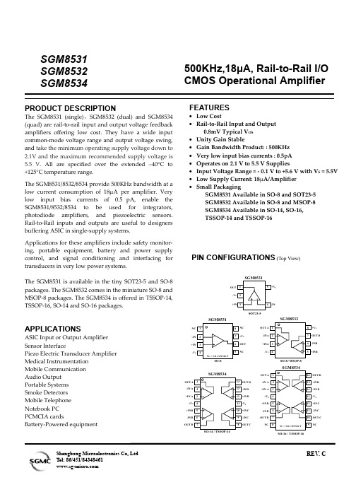
SGM8531 SGM8532 SGM8534PRODUCT DESCRIPTIONThe SGM8531 (single),SGM8532 (dual) and SGM8534 (quad) are rail-to-rail input and output voltage feedback amplifiers offering low cost. They have a wide input common-mode voltage range and output voltage swing, and take the minimum operating supply voltage down to 2.1V and the maximum recommended supply voltage is 5.5 V. All are specified over the extended –40°C to +125°C temperature range.The SGM8531/8532/8534 provide 500KHz bandwidth at a low current consumption of 18µA per amplifier. Very low input bias currents of 0.5pA, enable the SGM8531/8532/8534 to be used for integrators, photodiode amplifiers, and piezoelectric sensors. Rail-to-Rail inputs and outputs are useful to designers buffering ASIC in single-supply systems.Applications for these amplifiers include safety monitor- ing, portable equipment, battery and power supply control, and signal conditioning and interfacing for transducers in very low power systems.The SGM8531 is available in the tiny SOT23-5 and SO-8 packages. The SGM8532 comes in the miniature SO-8 and MSOP-8 packages. The SGM8534 is offered in TSSOP-14, TSSOP-16, SO-14 and SO-16 packages.APPLICATIONSASIC Input or Output Amplifier Sensor InterfacePiezo Electric Transducer Amplifier Medical Instrumentation Mobile Communication Audio Output Portable Systems Smoke Detectors Mobile Telephone Notebook PC PCMCIA cardsBattery-Powered equipment500KHz,18µA, Rail-to-Rail I/O CMOS Operational AmplifierFEATURES• Low Cost• Rail-to-Rail Input and Output0.8mV Typical V OS • Unity Gain Stable• Gain Bandwidth Product: : 500KHz • Very low input bias currents : 0.5pA • Operates on 2.1 V to 5.5 V Supplies• Input Voltage Range = - 0.1 V to +5.6 V with V S = 5.5V • Low Supply Current: 18µA/Amplifier • Small PackagingSGM8531 Available in SO-8 and SOT23-5 SGM8532 Available in SO-8 and MSOP-8 SGM8534 Available in SO-14, SO-16, TSSOP-14 and TSSOP-16PIN CONFIGURATIONS (Top View)S NC-V NC OUT S-V SOT23-5OUT B S -V SO-8 / MSOP-8OUT -IN A +IN A S +V -IN DD SO-16 / TSSOP-16-INB +IN B -IN C NCOUT BOUT C C D OUT +V -IN B +INB OUT BS -IN D+IN D -IN C OUT C+IN C OUT DShengbang Microelectronics Co, Ltd REV . CELECTRICAL CHARACTERISTICS : V S = +5V (At R L = 200kΩ connected to Vs/2 and V OUT = Vs/2, unless otherwise noted)Specifications subject to change without notice.PACKAGE/ORDERING INFORMATIONMODEL ORDER NUMBER PACKAGEDESCRIPTIONPACKAGE OPTION MARKING INFORMATIONSGM8531XN5/TRSOT23-5Tape and Reel, 30008531 SGM8531SGM8531XS/TR SO-8 Tape and Reel, 2500 SGM8531XS SGM8532XS/TR SO-8 Tape and Reel, 2500 SGM8532XS SGM8532SGM8532XMS/TRMSOP-8Tape and Reel, 3000SGM8532XMS SGM8534XS/TR SO-16 Tape and Reel, 2500SGM8534XSSGM8534XS14 SO-14Tube SGM8534XS14SGM8534XTS/TR TSSOP-16 Tape and Reel, 3000 SGM8534XTSSGM8534SGM8534XTS14 TSSOP-14TubeSGM8534XTS14ABSOLUTE MAXIMUM RATINGSSupply Voltage, V+ to V- ........................................... 7.5 VCommon-Mode Input Voltage.......................................... (–V S ) – 0.5 V to (+V S )+0.5VStorage Temperature Range.................. –65℃ to+150℃ Junction Temperature ................................................160℃ Operating Temperature Range ............ –55℃ to +150℃Package Thermal Resistance @ T A = 25℃SOT23-5, θJA .............................................................. 190/W ℃ SO-8, θJA ......................................................................125/W ℃ MSOP-8, θJA .............................................................. 216/W ℃ SO-16, θJA ..................................................................... 82/℃W TSSOP-16, θJA ............................................................ 105/W ℃ Lead Temperature Range (Soldering 10 sec).....................................................260℃ESD SusceptibilityHBM................................................................................4000V MM (400V)NOTES1. Stresses above those listed under Absolute Maximum Ratings may cause permanent damage to the device. This is a stress rating only; functional operation of the device at these or any other conditions above those indicated in the operational section of this specification is not implied. Exposure to absolute maximum rating conditions for extended periods may affect device reliability.CAUTIONThis integrated circuit can be damaged by ESD. Shengbang Micro-electronics recommends that all integrated circuits be handled with appropriate precautions. Failure to observe proper handling and installation procedures can cause damage.ESD damage can range from subtle performance degradation to complete device failure. Precision integrated circuits may be more susceptible to damage because very small parametric changes could cause the device not to meet its published specifications.TYPICAL PERFORMANCE CHARACTERISTICSAt T A = +25℃, V S = +5V , and R L =200k Ω connected to Vs/2,unless otherwise noted.Small-Signal Step Response Small-Signal Step Response10µs/div 10µs/divG = +1C L = 100pF R L = 5K ΩG = +1 C L = 100pF R L= 200K ΩG = +1 C L = 100pF R L= 200K Ω20m V /d i v50m V /d i v500m V /d i vLarge-Signal Step Response20µs/divTYPICAL PERFORMANCE CHARACTERISTICS At T A= +25℃, V S = +5V, and R L=200kΩ connected to Vs/2,unless otherwise noted.TYPICAL PERFORMANCE CHARACTERISTICSAt T A = +25℃, V S = +5V , and R L =200k Ω connected to Vs/2,unless otherwise noted.2.5V0V 250mV0VVs = 5V G = -10 V IN = 250mVTime(20μs/div)Overload Recovery TimeAPPLICATION NOTESDriving Capacitive LoadsThe SGM853X can directly drive 250pF in unity-gain without oscillation. The unity-gain follower (buffer) is the most sensitive configuration to capacitive loading. Direct capacitive loading reduces the phase margin of amplifiers and this results in ringing or even oscillation. Applications that require greater capacitive drive capability should use an isolation resistor between the output and the capacitive load like the circuit in Figure 1. The isolation resistor R ISO and the load capacitor C L form a zero to increase stability. The bigger the R ISO resistor value, the more stable V OUT will be. Note that this method results in a loss of gain accuracy because R ISO forms a voltage divider with the R LOAD.V IN V OUTFigure 1. Indirectly Driving Heavy Capacitive LoadAn improvement circuit is shown in Figure 2, It provides DC accuracy as well as AC stability. R F provides the DC accuracy by connecting the inverting signal with the output, C F and R Iso serve to counteract the loss of phase margin by feeding the high frequency component of the output signal back to the amplifier’s inverting input, thereby preserving phase margin in the overall feedback loop.V IN V OUTFigure 2. Indirectly Driving Heavy Capacitive Load with DC AccuracyFor no-buffer configuration, there are two others ways to increase the phase margin: (a) by increasing the amplifier’s gain or (b) by placing a capacitor in parallel with the feedback resistor to counteract the parasitic capacitance associated with inverting node. Power-Supply Bypassing and Layout The SGM853X family operates from either a single +2.5V to +5.5V supply or dual ±1.25V to ±2.75V supplies. For single-supply operation, bypass the power supply V DD with a 0.1µF ceramic capacitor which should be placed close to the V DD pin. For dual-supply operation, both the V DD and the V SS supplies should be bypassed to ground with separate 0.1µF ceramic capacitors. 2.2µF tantalum capacitor can be added for better performance.VnVpV SSV SS(GND)Figure 3. Amplifier with Bypass CapacitorsTypical Application Circuits Differential AmplifierThe circuit shown in Figure 4 performs the difference function. If the resistors ratios are equal ( R4 / R3 = R2 / R1 ), thenV OUT = ( Vp – Vn ) × R2 / R1 + Vref.Vn VpOUT Figure 4. Differential AmplifierInstrumentation AmplifierThe circuit in Figure 5 performs the same function as that in Figure 4 but with the high input impedance.Vn VpV OUT Figure 5. Instrumentation AmplifierLow Pass Active FilterThe low pass filter shown in Figure 6 has a DC gain of ( - R2 / R1 ) and the –3dB corner frequency is 1/2πR2C. Make sure the filter is within the bandwidth of the amplifier. The Large values of feedback resistors can couple with parasitic capacitance and cause undesired effects such as ringing or oscillation in high-speed amplifiers. Keep resistors value as low as possible and consistent with output loading consideration.V INV OUT Figure 6. Low Pass Active FilterPACKAGE OUTLINE DIMENSIONS SOT23-5PACKAGE OUTLINE DIMENSIONS SO-8PACKAGE OUTLINE DIMENSIONS MSOP-8PACKAGE OUTLINE DIMENSIONS SO-16PACKAGE OUTLINE DIMENSIONS TSSOP-16PACKAGE OUTLINE DIMENSIONS SO-14PACKAGE OUTLINE DIMENSIONS TSSOP-14REVISION HISTORYLocation Page 11/06— Data Sheet changed from REV.A to REV.BChanges to ABSOLUTE MAXIMUM ATINGS . . . . . . . . . . . . . . . . . . . . . . . . . . . . . . . .. . . . . . . . . . . . . . . . . . . . . . . . . . .. . . . . . . 3 05/07— Data Sheet changed from REV.B to REV.CAdds SO-14 and TSSOP-14 Package . . . . . . . . . . . . . . . . . . . . . . . . . . . . . . . . . . . . . . . . . . . . . . . .. . . . . . . . . . . . . . . . .. 1,3,14,15Shengbang Microelectronics Co, LtdUnit 3, ChuangYe PlazaNo.5, TaiHu Northern Street, YingBin Road Centralized Industrial ParkHarbin Development ZoneHarbin, HeiLongJiang 150078P.R. ChinaTel.: 86-451-84348461Fax: 86-451-84308461。
IRS2127PbF中文资料

Features•Floating channel designed for bootstrap operationFully operational to +600 V Tolerant to negative transient voltage dV/dt immune •Application-specific gate drive range:Motor Drive: 12 V to 20 V (IRS2127/IRS2128)Automotive: 9 V to 20 V (IRS21271/IRS21281)•Undervoltage lockout•3.3 V, 5 V, and 15 V input logic compatible • lead indicates shutdown has occured•Output in phase with input (IRS2127/IRS21271)•Output out of phase with input (IRS2128/IRS21281)CURRENT SENSING SINGLE CHANNEL DRIVERV OFFSET 600 V max. I O +/-200 mA / 420 mA V OUT 12 V - 20V 9 V - 20 V (IRS2127/IR2128) (IRS21271/IR21281) V CSth 250 mV or 1.8 V ton/off (typ.)150 ns & 150 nsTypical Connection 1Packages8-Lead PDIP 8-Lead SOICIRS212(7, 71, 8, 81)(S)PbFData Sheet No. PD 60299DescriptionThe IRS2127/IRS2128/IRS21271/IRS21281 arehigh voltage, high speed power MOSFET and IGBT drivers. Proprietary HVIC and latch immune CMOS technologies enable ruggedized monolithic construc-tion. The logic input is compatible with standard CMOS or LSTTL outputs, down to 3.3 V. The protec-tion circuity detects over-current in the driven power transistor and terminates the gate drive voltage. Anopen drain FAULT signal is provided to indicate that an over-current shutdown has occurred. The outputProduct Summarydriver features a high pulse current buffer stage designed for minimum cross-conduction. The floating chan-nel can be used to drive an N-channel power MOSFET or IGBT in the high-side or low-side configuration which operates up to 600 V.• RoHS compliantIRS212(7, 71, 8, 81)(S)PbF 2Absolute Maximum RatingsAbsolute maximum ratings indicate sustained limits beyond which damage to the device may occur. All voltage param-eters are absolute voltages referenced to COM. The thermal resistance and power dissipation ratings are measured Note 1: L ogic operational for V S of -5 V to +600 V. L ogic state held for V S of -5 V to -V BS . (Please refer to the Design Tip DT97-3 for more details).Recommended Operating ConditionsThe input/output logic timing diagram is shown in Fig. 1. For proper operation the device should be used within the recommended conditions. The V S offset rating is tested with all supplies biased at 15 V differential. 3IRS212(7, 71, 8, 81)(S)PbFDynamic Electrical CharacteristicsV BIAS (V CC , V BS ) = 15 V, C L = 1000 pF and T A = 25 °C unless otherwise specified. The dynamic electrical characteristics are measured using the test circuit shown in Fig. 3.Static Electrical CharacteristicsV BIAS (V CC , V BS ) = 15 V and T A = 25 °C unless otherwise specified. The V IN , V TH, and I IN parameters are referenced toIRS212(7, 71, 8, 81)(S)PbF 4Functional Block Diagram IRS2127/IRS21271Functional Block Diagram IRS2128/IRS21281IRS212(7, 71, 8, 81)(S)PbF5IRS212(7, 71, 8, 81)(S)PbF 6Figure 4. CS Shutdown Waveform DefinitionsFigure 5. CS to FAULT Waveform DefinitionsFigure 2. Switching Time Waveform DefinitionFigure 1. Input/Output Timing DiagramHOCSFAULTIRS21271)Figure 3. Start-U p Blanking Time WaveformDefinitionsFAULTIRS212(7, 71, 8, 81)(S)PbF7IRS212(7, 71, 8, 81)(S)PbF 80102030405060708090-50-25255075100Temperature (°C)Figure 9A. Turn-Off Fall Time vs.T u r n -O f f F a l l T i m e (n s )TemperatureIRS212(7, 71, 8, 81)(S)PbF9IRS212(7, 71, 8, 81)(S)PbF 10IRS212(7, 71, 8, 81)(S)PbF11IRS212(7, 71, 8, 81)(S)PbF 12IRS212(7, 71, 8, 81)(S)PbF13IRS212(7, 71, 8, 81)(S)PbF 14IRS212(7, 71, 8, 81)(S)PbF15IRS212(7, 71, 8, 81)(S)PbF 16IRS212(7, 71, 8, 81)(S)PbF 17IRS212(7, 71, 8, 81)(S)PbF18Case outlinesIRS212(7, 71, 8, 81)(S)PbF20CTape & Reel 8-lead SOIC 21IRS212(7, 71, 8, 81)(S)PbFORDER INFORMATION8-Lead PDIP IRS2127PbF 8-Lead PDIP IRS21271PbF 8-Lead SOIC IRS2127SPbF 8-Lead SOIC IRS21271SPbF8-Lead SOIC Tape & Reel IRS2127STRPbF 8-Lead SOIC Tape & Reel IRS21271STRPbFLEADFREE PART MARKING INFORMATIONPer SCOP 200-002The SOIC-8 is MSL2 qualified.This product has been designed and qualified for the industrial level.Qualification standards can be found at IR WORLD HEADQUARTERS: 233 Kansas St., El Segundo, California 90245 Tel: (310) 252-7105Data and specifications subject to change without notice. 6/27/20078-Lead PDIP IRS2128PbF 8-Lead PDIP IRS21281PbF 8-Lead SOIC IRS2128SPbF 8-Lead SOIC IRS21281SPbF8-Lead SOIC Tape & Reel IRS2128STRPbF 8-Lead SOIC Tape & Reel IRS21281STRPbF元器件交易网。
AiP31520中文资料

编号:AiP31520-AX-BJ-09
V2,V3,V5 COM0~COM15 SEG 61~ SEG 76 V1,V4,M/S SEG 77~ SEG 79 SEG0~SEG60 VDD VSS
CL OSC2
FR
I/O 缓冲 器
显示 起始行 寄存器 行计 数器
行地 址译码 器
i-core LCD驱动电路
9.5 15.0 uA
*14
5.0 10.0
IDD(2) tcyc==200KHz
COM5 COM6 COM7 COM8 COM9 COM10 COM11 COM12 COM13 COM14 COM15 SEG60 SEG59 SEG58 SEG57 SEG56 SEG55 SEG54 SEG53 SEG52 SEG51 SEG50 SEG49 SEG48 SEG47 SEG46 SEG45 SEG44 SEG43 SEG42
表 733-11-I
无锡中微爱芯电子有限公司
Wuxi I-CORE Electronics Co., Ltd.
编号:AiP31520-AX-BJ-09
3.2、电气特性
3.2.1、直流特性(VDD=0V,Ta=-20~75℃)
参数
符号
条件
最小 典型 最大 单位 对应管脚
电源电压(1)*1
推荐
-5.5 -5.0 -4.5
IOH=-3.0mA IOH=-2.0mA IOH=-120uA IOL=3.0mA IOL=2.0mA IOL=120uA
-13.0 -13.0 0.6×V5
V5 VSS+2.0 0.2×VSS
VSS VSS VSS+2.4 VSS+2.4 0.2×VSS
TC2117-2.5DBTR资料

Package Types
Tab is VOUT
3-Pin SOT-223 Front View
TC2117
1
2
3
VIN VOUT GND
3-Pin DDPAK Front View Tab is VOUT
TC2117
12 3
GND VOUT
VIN
© 2006 Microchip Tecpout voltage is defined as the input-to-output differential at which the output voltage drops 2% below its nominal value measured at a 1.5V differential.
TCVOUT
=
-(--V----O----U---T---M-----A---X----–-----V---O----U----T---M----I--N----)---–-----1---0---6VOUT × ΔT
4: Regulation is measured at a constant junction temperature using low duty cycle pulse testing. Load regulation is tested over a load range from 0.1 mA to the maximum specified output current. Changes in output voltage due to heating effects are covered by the thermal regulation specification.
- 1、下载文档前请自行甄别文档内容的完整性,平台不提供额外的编辑、内容补充、找答案等附加服务。
- 2、"仅部分预览"的文档,不可在线预览部分如存在完整性等问题,可反馈申请退款(可完整预览的文档不适用该条件!)。
- 3、如文档侵犯您的权益,请联系客服反馈,我们会尽快为您处理(人工客服工作时间:9:00-18:30)。
8.0
2CL71
1 of 1
VOLTAGE RANGE: 8 KV
Outline Drawings :
mm
27 min.
27 min.
6.5
o 2.5o 0.5
Cathode Mark
Lot No.
2CL71
25
5.0
CURRENT: 5.0 m A
High speed switching
High Current
High surge resisitivity for CRT discharge
High reliability design
High Voltage
X light Power supply
Laser
Voltage doubler circuit
Microwave emission power
Features
Applications
·
·
·
·
·
·
·
·
·
PLASTIC FAST RECOVER HIGH VOLTAGE RECITFIER
5.0
1.0
0.5
100
Repetitive Peak Renerse Voltage
Average Output Current
Suege Current
Junction Temperature
Allowable Operation Case Temperature
Symbols
V
RRM
I
O
I
FSM
T
j
Tc
Ta=25°C,Resistive Load
125
125
-40 to +125
Units
kV
mA
A
°C
°C
°C
Maximum Forward Voltage Drop
Maximum Reverse Current
V
F
V
uA
uA
R
stg
2.0
pF
RRM
nS
at 25°C,I
F
=I
F(AV)
Characteristic
Maximum Reverse Recovery Time
Trr
at 25°C
Junction Capacitance Cj at 25°C,V=0V,f=1MHz
V
at 100°C
at 25°C
Maximum Ratings and Electrical Characteristics
TA= 25°C unless otherwise specified
Storage Temperature T