RF3807中文资料
S-AV38中文资料
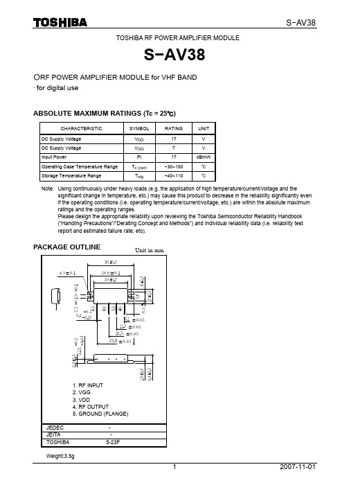
TOSHIBA RF POWER AMPLIFIER MODULES−AV38○RF POWER AMPLIFIER MODULE for VHF BAND·for digital useABSOLUTE MAXIMUM RATINGS (Tc = 25℃)CHARACTERISTIC SYMBOLUNITRATINGDC Supply Voltage V DD 17 VDC Supply Voltage V GG 7 VInput Power Pi 17 dBmWOperating Case Temperature Range T c (opr)−30~100 ℃Storage Temperature Range T stg−40~110 ℃Note: Using continuously under heavy loads (e.g. the application of high temperature/current/voltage and the significant change in temperature, etc.) may cause this product to decrease in the reliability significantly even if the operating conditions (i.e. operating temperature/current/voltage, etc.) are within the absolute maximum ratings and the operating ranges.Please design the appropriate reliability upon reviewing the Toshiba Semiconductor Reliability Handbook(“Handling Precautions”/“Derating Concept and Methods”) and individual reliability data (i.e. reliability testreport and estimated failure rate, etc).Weight:3.5gELECTRICAL CHARACTERISTICS (Tc = 25℃, Z G = 50Ω)CHARACTERISTIC SYMBOLTEST CONDITION MIN. TYP. MAX.UNITFrequency Range f range — 260 — 266MHzOutput PowerPoV DD = 7.2V, Po=35dBmW(Pi=adjust)I DD =1.7A(V GG = adjust) , Z L = 50Ω After that Pi = 15dBmW38.8 — — dBmWInput Power Pi V DD = 7.2V, I DD = 1.7A (V GG = adjust) Po = 35dBmW(Pi=adjust), Z L = 50Ω— — 5 dBmW Gate Bias VoltageV GG V DD = 7.2V, I DD = 1.7A (V GG = adjust) Po = 35dBmW(Pi=adjust), Z L = 50Ω 2.5 — 3.5 VGate Bias Current I GGBiasV DD = 7.2V, I DD = 1.7A (V GG = adjust) Po = 35dBmW (Pi= adjust), Z L = 50Ω After that Pi OFF— — 1 mAAdjacent-Channel Power Ratio ACP V DD = 7.2V, I DD = 1.7A (V GG = adjust) Po = 35dBmW (Pi= adjust), Z L = 50Ω Modulated Wave :π/4·DQPSK (α=0.5, 32kbps) Band Width : 16kHz Frequency Offset : 25kHz— — -35 dBSecond Harmonic 2nd HRM — — -27 dBThird Harmonic3rd HRM— — -30 dB Harmonic HRM V DD = 7.2V, I DD = 1.7A (V GG = adjust)Po = 35dBmW (Pi= adjust), Z L = 50Ω— — -35 dB Rate of Adjustment for Input Load VSWRin Input VSWR ( When RF output pin connects 50Ω Load )— — 3 — Rate of Adjustment for Output LoadVSWRoutInput VSWR ( When RF input pin connects 50Ω Load )— — 2.5 —Ralative Phase Variation—V DD = 7.2V, I DD = 1.7A (V GG = adjust)Po = 5 to 35dBmW (Pi= adjust) Z L = 50Ω(@ Po = 35dBmW)— — ±12°Load Mismatch—V DD = 7.2V, I DD = 1.7A (V GG = adjust)Po = 35dBmW (Pi= adjust, Z L = 50Ω) VSWR LOAD 20: 1 ALL PHASE No Degradation —Stability — V DD = 6.0 to 9.0V, V GG = 1 to 5VPi = -40 to 13 dBmWVSWR LOAD 3: 1 ALL PHASEAll spurious output than 60dB below desired signal—Caution・ This product has intersetting cap. Please pay attention for exceeding stress and foreign matter in your application. And not to take away the cap.・ Do not break, cut, crush or dissolve chemically. Dispose of this product properly according to law.Do not intermingle with normal industrial or domestic waste.・ This product is electrostatic sensitivity, please handle with caution.SCHEMATICTEST FIXTUREL L C1C1C1 : 10000pFC2 : 10μF L : φ0.8 ENAMEL WIRE 8T 5IDC2C21. PiZ G =50Ω4. PoZ L =50Ω2. V GG3. V DD(FLANGE)RESTRICTIONS ON PRODUCT USE20070701-EN GENERAL •The information contained herein is subject to change without notice.•TOSHIBA is continually working to improve the quality and reliability of its products. Nevertheless, semiconductor devices in general can malfunction or fail due to their inherent electrical sensitivity and vulnerability to physical stress. It is the responsibility of the buyer, when utilizing TOSHIBA products, to comply with the standards of safety in making a safe design for the entire system, and to avoid situations in which a malfunction or failure of such TOSHIBA products could cause loss of human life, bodily injury or damage to property.In developing your designs, please ensure that TOSHIBA products are used within specified operating ranges as set forth in the most recent TOSHIBA products specifications. Also, please keep in mind the precautions and conditions set forth in the “Handling Guide for Semiconductor Devices,” or “TOSHIBA Semiconductor Reliability Handbook” etc.• The TOSHIBA products listed in this document are intended for usage in general electronics applications (computer, personal equipment, office equipment, measuring equipment, industrial robotics, domestic appliances, etc.).These TOSHIBA products are neither intended nor warranted for usage in equipment that requires extraordinarily high quality and/or reliability or a malfunction or failure of which may cause loss of human life or bodily injury (“Unintended Usage”). Unintended Usage include atomic energy control instruments, airplane or spaceship instruments, transportation instruments, traffic signal instruments, combustion control instruments, medical instruments, all types of safety devices, etc.. Unintended Usage of TOSHIBA products listed in his document shall be made at the customer’s own risk.•The products described in this document shall not be used or embedded to any downstream products of which manufacture, use and/or sale are prohibited under any applicable laws and regulations.• The information contained herein is presented only as a guide for the applications of our products. No responsibility is assumed by TOSHIBA for any infringements of patents or other rights of the third parties which may result from its use. No license is granted by implication or otherwise under any patents or other rights of TOSHIBA or the third parties.• Please contact your sales representative for product-by-product details in this document regarding RoHS compatibility. Please use these products in this document in compliance with all applicable laws and regulations that regulate the inclusion or use of controlled substances. Toshiba assumes no liability for damage or losses occurring as a result of noncompliance with applicable laws and regulations.。
FR38中文资料
Data Sheet
3.0 Amp FAST RECOVERY PLASTIC RECTIFIERS
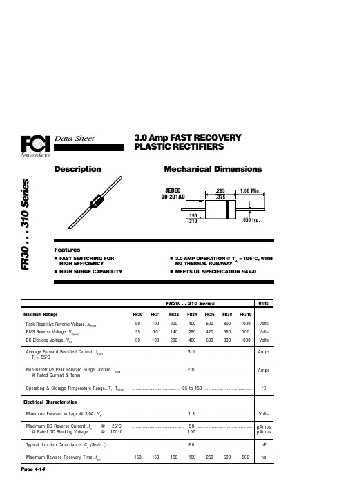
Mechanical Dimensions
JEDEC D0-201AD
.190 .210 .285 .375 1.00 Min.
Description
FR30 . . . 310 Series
NOTES: 1. Measured @ 1 MHz and applied reverse voltage of 4.0V. 2. Thermal Resistance Junction to Case, Jedec Method.
Page 4-15
FR30 . . . 310 Series
Oscilliscope Note 1
(+)
0A -.25A
Notes: 1 . Rise Time = 7 ns Max. Impedance = 1 megohm, 22 pF 2 . Rise Time = 10 ns Max. Source Impedance = 50 Ohms
-1.0A
1 cm Time Base Set @ 50/100ns/cm
FR30. . . 310 Series Maximum Ratings Peak Repetitive Reverse Voltage...VRRM RMS Reverse Voltage...VR(rms) DC Blocking Voltage...VDC Average Forward Rectified Current...IF(av) TA = 55°C Non-Repetitive Peak Forward Surge Current...IFSM @ Rated Current & Temp Operating & Storage Temperature Range...TJ, TSTRG Electrical Characteristics Maximum Forward Voltage @ 3.0A...VF Maximum DC Reverse Current...IR @ Rated DC Blocking Voltage @ @ 25°C 100°C ............................................. 1.3 ............................................... FR30 50 35 50 FR31 100 70 100 FR32 200 140 200 FR34 400 280 400 FR36 600 420 600 FR38 800 560 800 FR310 1000 700 1000
OP07C中文资料

OP07C中文资料一、Op07芯片是一种低噪声,非斩波稳零的单运算放大器集成电路。
由于OP07具有非常低的输入失调电压(对于OP07A最大为25μV),所以OP07在很多应用场合不需要额外的调零措施。
OP07同时具有输入偏置电流低(OP07A为±2nA)和开环增益高(对于OP07A 为300V/mV)的特点,这种低失调、高开环增益的特性使得OP07特别适用于高增益的测量设备和放大传感器的微弱信号等方面。
二、OP07特点:超低偏移: 150μV最大。
低输入偏置电流: 1.8nA 。
低失调电压漂移: 0.5μV/℃。
超稳定,时间: 2μV/month最大高电源电压范围:±3V至±22V三、OP07内部结构原理图四、OP07芯片引脚功能说明:1和8为偏置平衡(调零端),2为反向输入端,3为正向输入端,4接地,5空脚 6为输出,7接电源+ABSOLUTE MAXIMUM RATINGS 最大额定值五、OP07典型应用电路图4 输入失调电压调零电路图5 典型的偏置电压试验电路图6 老化电路图7 典型的低频噪声放大电路图8 高速综合放大器图9 选择偏移零电路图10 调整精度放大器图11高稳定性的热电偶放大器图12 精密绝对值电路op07的功能介绍:Op07芯片是一种低噪声,非斩波稳零的双极性运算放大器集成电路。
由于OP07具有非常低的输入失调电压(对于OP07A 最大为25μV),所以OP07在很多应用场合不需要额外的调零措施。
OP07同时具有输入偏置电流低(OP07A为±2nA)和开环增益高(对于OP07A为300V/mV)的特点,这种低失调、高开环增益的特性使得OP07特别适用于高增益的测量设备和放大传感器的微弱信号等方面。
特点:超低偏移: 150μV最大。
低输入偏置电流: 1.8nA 。
低失调电压漂移: 0.5μV/℃。
超稳定,时间: 2μV/month最大高电源电压范围:±3V至±22V工作电源电压范围是±3V~±18V;OP07完全可以用单电源供电,你说的+5V,-5V绝对没有问题,用单+5V也可以供电,但是线性区间太小,单电源供电,模拟地在1/2 VCC. 建议电源最好>8V,否则线性区实在太小,放大倍数无法做大,一不小心,就充顶饱和了。
MP2307中文资料
ELECTRICAL CHARACTERISTICS
VIN = 12V, TA = +25°C, unless otherwise noted.
Parameter
© 2006 MPS. All Rights Reserved.
元器件交易网
TM
MP2307 – 3A, 23V, 340KHz SYNCHRONOUS RECTIFIED STEP-DOWN CONVERTER
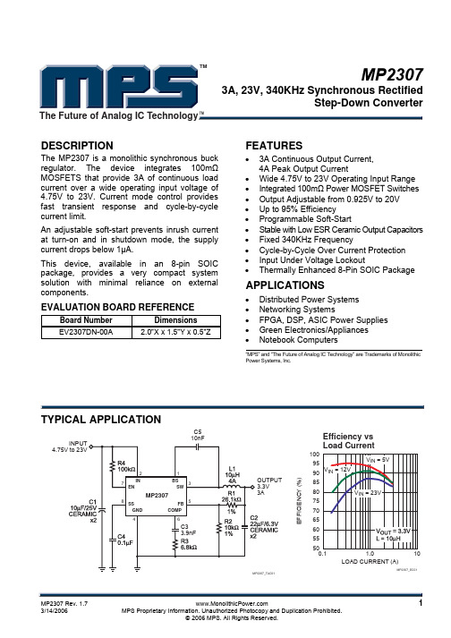
TYPICAL PERFORMANCE CHARACTERISTICS
© 2006 MPS. All Rights Reserved.
元器件交易网
TM
MP2307 – 3A, 23V, 340KHz SYNCHRONOUS RECTIFIED STEP-DOWN CONVERTER
PACKAGE REFERENCE
TOP VIEW
BS 1 IN 2 SW 3 GND 4
100
95 90 VIN = 12V
VIN = 5V
85
80
VIN = 23V
75
70
65
60
55
50
0.1
1.0
10
LOAD CURRENT (A)
MP2307_EC01
MP2307 Rev. 1.7
1
3/14/2006
MPS Proprietary Information. Unauthorized Photocopy and Duplication Prohibited.
XC-RF807型读写器用户手册

前言
本手册适用于以下型号产品: XC-RF807型读写器 XC-RF807-FBT型读写器(基本型号增加蓝牙通讯功能) 本手册提供了产品的安装、使用、维护维修及其它特征信息,可供产品的安装 人员、使用人员、维修人员阅读使用。手册以基本型号为介绍对象,扩展型号 新增功能以提示作为说明。
或
标识,均为远望谷公司所有。
五、售后................................................. 41 1.售后服务.................................................... 41 2.其它说明事项................................................ 41
图1.1 XC-RF807型读写器 XC-RF807型读写器的组成各部分说明如下: 1- 上盖
XC-RF807型读写器
2 用户手册
2- 导光柱 3- 防水贴纸 4- 电路板 5- 射频接头 6- 盘头螺丝 7- 底板 8- 防水圈 9- 沉头螺丝 10- 防滑脚垫 11- 铭牌
2.主要用途及适用范围
本手册中所有关于产品特性和功能的介绍及说明,以及其它信息都是当时最新 的有效信息,且所有信息在印刷时均准确无误。远望谷公司将保留对本手册更 正或更改其中信息及说明的权力,恕不另行通知而不承担任何责任。
XC-RF807型读写器
1 用户手册
一、产品概述
1.产品的组成、功能及特点
XC-RF807型读写器是一款符合ISO18000-6C (EPC global UHF Class 1 Gen 2) 和ISO18000-6B双协议标准,具有高性能、宽频段及可扩展性的UHF RFID读写 设备。该设备具有较强的多标签读取能力,支持网络供电(POE)等特点,具 有可靠的网络适应性,适用于多读写器组网应用。XC-RF807型读写器的结构分 解图如下所示:
LM3880MFX-1AB资料

LM3880Power SequencerGeneral DescriptionThe LM3880Power Sequencer offers the easiest method to control power up and power down of multiple power supplies (switchers or linear regulators).By staggering the startup sequence,it is possible to avoid latch conditions or large in-rush currents that can affect the reliability of the system. Available in a SOT23-6package,the Power Sequencer contains a precision enable pin and three open drain output flags.Upon enabling the LM3880the three output flags will sequentially release,after individual time delays,permitting the connected power supplies to startup.The output flags will follow a reverse sequence during power down to avoid latch conditions.Standard timing option of30ms is available.EPROM capability allows every delay and sequence to be fully adjustable.Contact National Semiconductor if a non-standard configuration is required.Featuresn Easiest method to sequence railsn Power up and power down controln Input voltage range of2.7V to5.5Vn Small footprint SOT23-6n Low quiescent current of20µAn Standard timing options availablen Customization of timing and sequence available through factory programmabilityApplicationsn Multiple supply sequencingn Microprocessor/Microcontroller sequencingn FPGA sequencingTypical Application Circuit20192601September2006LM3880Power Sequencer©2006National Semiconductor Corporation Connection Diagram20192602Top ViewSOT23–6PackagePin DescriptionsPin #Name Function 1VCC Input supply 2GND Ground 3EN Precision enable pin 4FLAG3Open drain output #35FLAG2Open drain output #26FLAG1Open drain output #1Ordering Information20192603Sequence Designator TableSequence NumberFlag OrderPower Up Power Down 11-2-33-2-121-2-33-1-231-2-32-3-141-2-32-1-351-2-31-3-261-2-31-2-3See timing diagrams for more informationL M 3880 2Ordering Information(Continued)Timing Designator TableTimingDesignator t d1t d2t d3t d4t d5t d6 AA10ms10ms10ms10ms10ms10ms AB30ms30ms30ms30ms30ms30ms AC60ms60ms60ms60ms60ms60ms AD120ms120ms120ms120ms120ms120ms See timing diagrams for more informationLM3880Ordering InformationOrder NumberTimer settingsSequenceOrder Supplied AsPackageTypeNSCPackageDrawingPackageMarking t d1t d2t d3t d4t d5t d6LM3880MF-1AB30ms30ms30ms30ms30ms30ms11k units T&R SOT23-6MF06A F21ALM3880MFX-1AB30ms30ms30ms30ms30ms30ms13k units T&R SOT23-6MF06A F21A Non-standard parts are available upon request.Please contact National Semiconductor for more information.LM38803Absolute Maximum Ratings (Note 1)If Military/Aerospace specified devices are required,please contact the National Semiconductor Sales Office/Distributors for availability and specifications.VCC−0.3V to +6.0V EN,FLAG1,FLAG2,FLAG3−0.3V to +6.0V Storage Temperature Range −65˚C to +150˚CJunction Temperature150˚C Lead Temperature (Soldering,5sec.)260˚CMinimum ESD Rating±2kVOperating Ratings (Note 1)VCC to GND 2.7V to 5.5V Junction Temperature−40˚C to +125˚CElectrical CharacteristicsSpecifications with standard typeface are for T J =25˚C,and those in bold facetype apply over the full Operating Temperature Range (T J =-40˚C to +125˚C).Minimum and Maximum limits are guaranteed through test,design or statistical correlation.Typical values represent the most likely parametric norm at T J =25˚C and are provided for reference purposes only.Unless otherwise specified VCC =3.3V.Symbol ParameterConditions Min (Note 3)Typ (Note 4)Max (Note 3)Unit I QOperating Quiescent current 2080µA Open Drain FlagsI FLAG FLAGx Leakage Current V FLAGx =3.3V 120nA V OLFLAGx Output Voltage Low I FLAGx =1.2mA0.4V Power Up Sequencet d1Timer delay 1accuracy -1515%t d2Timer delay 2accuracy -1515%t d3Timer delay 3accuracy -1515%Power Down Sequencet d4Timer delay 4accuracy -15_15%t d5Timer delay 5accuracy -1515%t d6Timer delay 6accuracy -1515%Timing Delay Error (t d(x)–400us)/t d(x+1)Ratio of timing delays For x =1or 495105%t d(x)/t d(x+1)Ratio of timing delays For x =2or 595105%ENABLE PinV EN EN pin threshold 0.91.4V I ENEN pin pull-up currentV EN =0V16µANote 1:Absolute Maximum Ratings indicate limits beyond which damage to the device may occur.Operating Ratings indicate conditions for which the device is intended to be functional,but does not guarantee specific performance limits.For guaranteed specifications and conditions,see the Electrical Characteristics.Note 2:The human body model is a 100pF capacitor discharged through a 1.5k Ωresistor into each pin.Note 3:Limits are 100%production tested at 25˚.Limits over the operating temperature range are guaranteed through correlation using Statistical Quality Control (SQC)methods.The limits are used to calculate National’s Average Outgoing Quality Level (AOQL).Note 4:Typical numbers are at 25˚C and represent the most likely parametric norm.L M 3880 4Typical Performance CharacteristicsQuiescent Current vs VCCQuiescent Current vs Temperature (VCC =3.3V)2019260420192605Enable Threshold vs Temperature Time Delay (30ms)vs VCC2019260620192607Time Delay Ratio vs Temperature Time Delay (30ms)vs Temperature2019260820192609LM38805Typical Performance Characteristics(Continued)FLAG V OL vs VCC (R FLAG =100k Ω)FLAG Voltage vs Current2019261020192611L M 3880 6Block DiagramBlock Diagram20192612Timing Diagrams (Sequence 1)All standard options use this sequence for output flags rise and fall order.20192613Power Up SequenceLM38807Timing Diagrams (Sequence 1)(Continued)20192614Power Down SequenceApplication InformationOVERVIEWThe LM3880Power Sequencer provides an easy solution for sequencing multiple rails in a controlled manner.Six inde-pendent timers are integrated to control the timing sequence (power up and power down)of three open drain output flags.These flags permit connection to either a shutdown /enable pin of linear regulators and switchers to control the power supplies’operation.This allows a complete power system to be designed without worrying about large in-rush currents or latch-up conditions that can occur.The timing sequence of the LM3880is controlled entirely by the enable (EN)pin.Upon power up,all the flags are held low until this precision enable is pulled high.After the EN pin is asserted,the power up sequence will commence.An internal counter will delay the first flag (FLAG1)from rising until a fixed time period has expired.Upon the release of the first flag another timer will begin to delay the release of the second flag (FLAG2).This process repeats until all three flags have sequentially been released.The three timers that control the delays are all independent of each other and can be individually programmed if needed.(See custom se-quencer section).The power down sequence is the same as power-up,but in reverse.When EN pin is de-asserted a timer will begin that delays the third flag (FLAG3)from pulling low.The second and first flag will then follow in a sequential manner after their appropriate delays.The three timers that are used to control the power down scheme can also be individually pro-grammed and are completely independent of the power up timers.Additional sequence patterns are also available in addition to customizable timers.For more information see the custom sequencer section.PART OPERATIONThe timing sequence of the LM3880is controlled by the assertion of the enable signal.The enable pin is designed with an internal comparator,referenced to a bandgap volt-age (1.15V),to provide a precision threshold.This allows a delayed timing to be externally set using a capacitor or to start the sequencing based on a certain event,such as a line voltage reaching 90%of nominal.For an additional delayed sequence from the rail powering VCC,simply attach a ca-pacitor to the EN pin as shown below.20192615Cap TimingUsing the internal pull-up current source to charge the ex-ternal capacitor (C EN )the enable pin delay can be calculated by the equation below:A resistor divider can also be used to enable the LM3880based on a certain voltage threshold.Care needs to be taken when sizing the resistor divider to include the effects of the internal current source.One of the features of the enable pin is that it provides glitch free operation.The first timer will start counting at a rising threshold,but will always reset if the enable pin is de-asserted before the first output flag is released.This can be shown in the timing diagram below:L M 3880 8Application Information(Continued)20192617EN GlitchIf the enable signal remains high for the entire power-up sequence,then the part will operate as shown in the stan-dard timing diagrams.However,if the enable signal is de-asserted before the power-up sequence is completed the part will enter a controlled shutdown.This allows the system to walk through a controlled power cycling,preventing any latch conditions from occuring.This state only occurs if the enable pin is de-asserted after the completion of timer1,but before the entire power-up sequence is completed.When this event occurs,the falling edge of enable pin resets the current timer and will allow the remaining power-up cycle to complete before beginning the power down sequence. The power down sequence starts approximately120ms after the final power-up flag.This allows output voltages in the system to stabilize before everything is shutdown.An ex-ample of this operation can be seen below:20192618Incomplete SequenceAll the internal timers are generated by a master clock that has an extremely low tempco.This allows for tight accuracy across temperature and a consistent ratio between the indi-vidual timers.There is a slight additional delay of approxi-mately400us to timers1and4which is a result of the EPROM refresh.This refresh time is in addition to the pro-grammed delay time and will be almost insignificant to all but the shortest of timer delays.CUSTOM SEQUENCERThe LM3880Power Sequencer is based on a CMOS pro-cess utilizing an EPROM that has the capability to be customprogrammed at the factory.Approximately500,000,000dif-ferent options are available allowing even the most complexsystem to be simply sequenced.Because of the vast optionsthat are possible,customization is limited to orders of acertain quantity.Please contact National Semiconductor formore information.The variables that can be programmed include the six delaytimers and the reverse sequence order.For the timers,eachcan be individually selected from one of the timer selectorcolumns in the table shown below.However,all six timedelays must be from the same column.LM38809Application Information(Continued)Timer Options 1Timer Options 2Timer Options 3Timer Options 400002468481216612182481624321020304012243648142842561632486418365472204060802244668824487296265278104285684112306090120All times listed are in millisecondsThe sequencing order for power up is always controlled by layout.The flag number translates directly into the sequence order during power up (ie FLAG1will always be first).How-ever,for some systems a different power down order could be required.To allow flexibility for this aspect in a design,thePower Sequencer incorporates six different options for con-trolling the power down sequence.These options can be seen in the timing diagrams on the next page.This ability can be programmed in addition to the custom timers.L M 3880 10LM3880 Application Information(Continued)20192619Power Down Sequence Options11Physical Dimensionsinches (millimeters)unless otherwise notedSOT23-6PackageNS Package Number MF06ANational does not assume any responsibility for use of any circuitry described,no circuit patent licenses are implied and National reserves the right at any time without notice to change said circuitry and specifications.For the most current product information visit us at .LIFE SUPPORT POLICYNATIONAL’S PRODUCTS ARE NOT AUTHORIZED FOR USE AS CRITICAL COMPONENTS IN LIFE SUPPORT DEVICES OR SYSTEMS WITHOUT THE EXPRESS WRITTEN APPROVAL OF THE PRESIDENT AND GENERAL COUNSEL OF NATIONAL SEMICONDUCTOR CORPORATION.As used herein:1.Life support devices or systems are devices or systems which,(a)are intended for surgical implant into the body,or (b)support or sustain life,and whose failure to perform when properly used in accordance with instructions for use provided in the labeling,can be reasonably expected to result in a significant injury to the user.2.A critical component is any component of a life support device or system whose failure to perform can be reasonably expected to cause the failure of the life support device or system,or to affect its safety or effectiveness.BANNED SUBSTANCE COMPLIANCENational Semiconductor follows the provisions of the Product Stewardship Guide for Customers (CSP-9-111C2)and Banned Substances and Materials of Interest Specification (CSP-9-111S2)for regulatory environmental compliance.Details may be found at:/quality/green.Lead free products are RoHS compliant.National Semiconductor Americas Customer Support CenterEmail:new.feedback@ Tel:1-800-272-9959National SemiconductorEurope Customer Support CenterFax:+49(0)180-5308586Email:europe.support@Deutsch Tel:+49(0)6995086208English Tel:+44(0)8702402171Français Tel:+33(0)141918790National Semiconductor Asia Pacific Customer Support CenterEmail:ap.support@National SemiconductorJapan Customer Support Center Fax:81-3-5639-7507Email:jpn.feedback@ Tel:81-3-5639-7560L M 3880P o w e r S e q u e n c e r。
ADS807中文资料

12位,采样频率53兆的A/D转换器一、特点:1.无杂散动态范围:输入频率为10MHz时为82dB。
2.高信噪比:67.5dB(2v p-p),69dB(3V p-p)。
3.低功率:335mW。
4.有内部或外部参考5.低微分非线性:0.5LSB。
6.输入范围灵活:2V p-p到3V p-p。
7.28管脚封装二、应用:1.处理过程中的通信2.通信基站3.测试装备4.医疗成像5.视频数字化D数字化三、描述:ADS807是一个高速,宽动态范围,12位通道的数模转换器(A/D)。
这种数模转换器具有高带宽的跟踪和保持特性,而这种特性在奈奎斯特速率的附近表现出了良好的杂散性。
这种跟踪和保持特性的差分本质和A/D转换电路使偶次谐波最小化并且拥有良好的抗共模干扰能力。
而这种跟踪和保持特性一直具有直到信号结束。
ADS807在没有任何外部参考电路情况下,转换器的满量程都是可以使用的。
而内部的参考电路不支持低驱动,且内部的参考电路可以用来改善在多通道系统中的跟踪特性。
ADS807提供了一个超量程指示标志用来指示超出转换器输入满量程的输入信号,这个标志可以用来减少前端增益控制电路的增益。
且其存在一个输出使能管脚允许在PC板上实现复用和可测性。
ADS807采用数字误差校正技术,为需要图像处理的场合提供优良的差分线性。
绝对最大额定值:注意:列在上表“绝对最大额定值”中的这些重要参数可能对装置设备产生永久性的伤害。
长时间使用在绝对最大值的这种情况下可能会影响设备的可信度。
四、静电放电敏感度这个综合电路可能被ESD破坏。
TI公式推荐所有的综合电路要与适当的预防措施配合使用。
不遵守适当的处理和安装程序,可能会造成伤害。
ESD造成的破坏有很多,小到微弱的性能下降,大到整个装置的破坏。
精密的综合电路对这些破坏会更敏感,因为非常小的参数改变都可能引起装置不能满足其发布的规范。
包装/订购信息注意:(1)对于大部分当前的规范和包装信息查询我们的网站。
UC3879中文资料

UC3879移相PWM控制器简化了零电压过渡全桥变换器的设计拉兹洛巴洛格简介这篇操作说明书将介绍UC3879集成电路,并与它的前身UC3875/6/7/8作性能上的比较。
这些集成电路提供了所有必要的控制,解码,保护和驱动器的功能,成功地处理了移相控制全桥变换器的操作。
该集成解决方案,大大简化了设计过程,并为设计者显著的节省了研制时间和印刷电路板设计。
在中高功率直流到直流电源转换中,用传统的移相技术来控制全桥拓扑的优势已经被证明。
这种控制方法能在几乎所有的操作条件下提供很好的控制的dv / dt值和所有初级侧功率级半导体的零电压开关。
在[1-8]几个出版物中讨论了操作的细节,包括全桥变换器谐振转换的等效电路和零电压开关的实现条件并描述了进一步改善的可能性。
这种方法所提供的主要好处是比它对应的硬转换简单的功率级,通过利用电路寄生而不是任其造成损失来提高效率以及较低的电磁干扰。
这些显着的优势是通过一个稍微复杂的控制算法来实现的。
UNITRODE公司 UC3879相移PWM控制集成电路 - 框图UC3879是先前推出的UC3875控制器系列的改进版。
该IC的内部结构如图1所示。
UC3879的欠压锁定水平用户可由UVSEL引脚选择。
有两个预定义的阈值。
,如果UVSEL引脚是悬空的,当提供给VIN引脚的电压超过15.25V时芯片启动。
UVSEL引脚和VIN引脚外部连接的情况下,操作开在10.75V时开始。
不受支配的操作开始,当输入电压低于9.25V时,UC3879芯片为欠压锁定状态。
同步的振荡器的工作频率是由两个外部元件编程。
从RT引脚接地电阻定义定时电容的充电电流,放电电流是内部固定在10mA。
通过这种方式,相当于上出现在芯片CLKSYNC上的输出信号的占空比的(DOSC)振荡器占空比,可以在这样的基础关系上准确设置:推荐的最小运行可靠的脉冲宽度约为250ns,并且所有实际应用不应超过500ns.因此,应当依据时钟频率选择DOSC:CT引脚和地面之间的连接的定时电容值与已定义的RT值的组合,决定了时钟频率(CLOCK),按下列公式:在实践中,选择适当的电容值比电阻困难得多。
- 1、下载文档前请自行甄别文档内容的完整性,平台不提供额外的编辑、内容补充、找答案等附加服务。
- 2、"仅部分预览"的文档,不可在线预览部分如存在完整性等问题,可反馈申请退款(可完整预览的文档不适用该条件!)。
- 3、如文档侵犯您的权益,请联系客服反馈,我们会尽快为您处理(人工客服工作时间:9:00-18:30)。
4-623Product DescriptionOrdering InformationTypical ApplicationsFeaturesFunctional Block DiagramRF Micro Devices, Inc.7628 Thorndike RoadGreensboro, NC 27409, USATel (336) 664 1233Fax (336) 664 0454http://www.rfmd.comOptimum Technology Matching® AppliedSi BJTGaAs MESFETGaAs HBTSi Bi-CMOSSiGe HBTSi CMOSInGaP/HBTGaN HEMTSiGe Bi-CMOS12348765PACKAGE BASEGNDBiasCircuitVREFNCRFINNCVBIASNCRFOUT/VCCRFOUT/VCCRF3807GaAs HBT PRE-DRIVER AMPLIFIER•GaAs Pre-Driver for Basestation Amplifiers•PA Stage for Commercial Wireless Infrastructure•Class AB Operation for NMT, GSM, DCS, PCS, UMTS, and WLAN Transceiver ApplicationsThe RF3807 is a GaAs pre-driver power amplifier, specifi-cally designed for wireless infrastructure applications.Using a highly reliable GaAs HBT fabrication process,this high-performance single-stage amplifier achieveshigh output power over a broad frequency range. TheRF3807 also provides excellent efficiency and thermalstability through the use of a thermally-enhanced surface-mount plastic-slug package. Ease of integration is accom-plished through the incorporation of an optimized evalua-tion board design provided to achieve proper 50Ωoperation. Various evaluation boards are available toaddress a broad range of wireless infrastructure applica-tions: NMT 450MHz; GSM850; GSM900; DCS1800;PCS1900; UMTS2100; and, WLAN2400.•Output Power>0.5W P1dB•High Linearity•High Power-Added Efficiency•Thermally-Enhanced Packaging•Broadband Platform Design Approach, 450MHz to 2500MHzRF3807GaAs HBT Pre-Driver AmplifierRF3807PCK-410Fully Assembled Evaluation Board, 450MHzRF3807PCK-411Fully Assembled Evaluation Board, 869MHz to 894MHzRF3807PCK-412Fully Assembled Evaluation Board, 920MHz to 960MHzRF3807PCK-413Fully Assembled Evaluation Board, 1800MHz to 1880MHzRF3807PCK-414Fully Assembled Evaluation Board, 1930MHz to 1990MHzRF3807PCK-415Fully Assembled Evaluation Board, UMTS0Rev A4 0509120.0660.056-A-0.0040.0020.1260.088EXPOSEDDIE FLAG0.0990.0610.01920.01380.2440.230
0.1570.150
0.1960.189
0.050
0.0350.016
0.0098
0.0075
8° MAX0° MIN
Shaded lead is pin 1.
Package Style: SOIC-89
RoHS Compliant & Pb-Free Product元器件交易网www.cecb2b.com4-624RF3807Rev A4 050912
Absolute Maximum RatingsParameterRatingUnitSupply Voltage (VCC and VBIAS)9.0VPower Control Voltage (VREF)9.0V
DC Supply Current250mAMaximum Input Powersee belowOutput Load VSWR @ P1dB4:1Operating Ambient Temperature-40 to +85°CStorage Temperature-40 to +150°C
ParameterSpecificationUnitConditionMin.Typ.Max.
Overall - 450MHzFrequency420480MHzIREF=14mA, VCC=8V, VREF=8V, VBIAS=8V, Temp=+25°CP1dB+28.5+29.0+29.5dBmPIN, Maximum16dBm
Total Efficiency51.053.555.0%@P1dBTotal Power Added Efficiency50.052.554.0%@P1dBGain (S21)16.016.517.0dBSecond Harmonic (2fo)-21.0-19.0-18.5dBc@P1dBThird Harmonic (3fo)-25.0-21.0-20.0dBc@P1dBInput Return Loss (S11)-15.0-13.0-11.0dBOutput Return Loss (S22)-8.0-6.5-6.0dBTwo-Tone SpecificationOIP338.040.0dBm15dBm/tone39.542.0dBm17dBm/tone41.043.5dBm19dBm/tone42.544.5dBm21dBm/tone
Caution! ESD sensitive device.RF Micro Devices believes the furnished information is correct and accurate at the time of this printing. RoHS marking based on EUDirective2002/95/EC (at time of this printing). However, RF Micro Devices reserves the right to make changes to its products without notice. RF Micro Devices does not assume responsibility for the use of the described product(s).
元器件交易网www.cecb2b.com4-625RF3807Rev A4 050912ParameterSpecificationUnitConditionMin.Typ.Max.
Overall - GSM800Frequency869894MHzIREF=14mA, VCC=8V, VREF=8V, VBIAS=8V, Temp=+25°CP1dB+30.0+30.5+32.0dBmPIN, Maximum16dBm
Total Efficiency545660%@P1dBTotal Power Added Efficiency535559%@P1dBGain (S21)15.516.517.0dBSecond Harmonic (2fo)-25.0-20.0-18.0dBc@P1dBThird Harmonic (3fo)-44.0-39.0-35.0dBc@P1dBInput Return Loss (S11)-33.0-18.0-10.0dBOutput Return Loss (S22)-20.0-12.0-8.0dBTwo-Tone SpecificationOIP336.038.5dBm15dBm/tone38.041.0dBm17dBm/tone40.044.0dBm19dBm/tone43.045.0dBm21dBm/toneOverall - GSM900Frequency920960MHzIREF=14mA, VCC=8V, VREF=8V, VBIAS=8V, Temp=+25°CP1dB+30.0+30.5+31.0dBmPIN, Maximum16dBm
Total Efficiency545658%@P1dBTotal Power Added Efficiency535557%@P1dBGain (S21)16.016.517.0dBSecond Harmonic (2fo)-25.0-22.0-21.0dBc@P1dBThird Harmonic (3fo)-33.0-30.5-24.5dBc@P1dBInput Return Loss (S11)-29.0-22.0-9.0dBOutput Return Loss (S22)-10.0-8.5-7.5dBTwo-Tone SpecificationOIP341.542.5dBm15dBm/tone42.043.0dBm17dBm/tone41.544.0dBm19dBm/tone40.542.0dBm21dBm/tone