RLD-78MV中文资料
RLD78MPA1中文资料

10 −10
0
10
20
30
40
50
60
70
80
0 −40
0 ANGLE (deg)
40
PACKAGE TEMPERATURE : TC (°C)
Fig.1 Optical output vs. operating current
Fig.2 Threshold current vs. package temperature
LM78M12中文资料

LM78M12中⽂资料LM341/LM78MXX Series3-Terminal Positive Voltage RegulatorsGeneral DescriptionThe LM341and LM78MXX series of three-terminal positive voltage regulators employ built-in current limiting,thermal shutdown,and safe-operating area protection which makes them virtually immune to damage from output overloads.With adequate heatsinking,they can deliver in excess of 0.5A output current.Typical applications would include local (on-card)regulators which can eliminate the noise and de-graded performance associated with single-point regulation.Featuresn Output current in excess of 0.5A n No external componentsn Internal thermal overload protection n Internal short circuit current-limitingn Output transistor safe-area compensationnAvailable in TO-220,TO-39,and TO-252D-PAK packagesn Output voltages of 5V,12V,and 15VConnection DiagramsTO-39Metal Can Package (H)DS010484-5Bottom ViewOrder Number LM78M05CH,LM78M12CH or LM78M15CHSee NS Package Number H03ATO-220Power Package (T)DS010484-6Top ViewOrder Number LM341T-5.0,LM341T-12,LM341T-15,LM78M05CT,LM78M12CT or LM78M15CTSee NS Package Number T03BTO-252DS010484-19Top ViewOrder Number LM78M05CDT See NS Package Number TD03BJuly 1999LM341/LM78MXX Series 3-Terminal Positive Voltage Regulators1999National Semiconductor Corporation /doc/96ef4d46852458fb770b5641.htmlAbsolute Maximum Ratings(Note1)If Military/Aerospace specified devices are required, please contact the National Semiconductor Sales Office/ Distributors for availability and specifications.Lead Temperature(Soldering,10seconds)TO-39Package(H)300?C TO-220Package(T)260?C Storage Temperature Range?65?C to+150?C Operating Junction TemperatureRange?40?C to+125?C Power Dissipation(Note2)Internally Limited Input Voltage5V≤V O≤15V35V ESD Susceptibility TBDElectrical CharacteristicsLimits in standard typeface are for T J=25?C,and limits in boldface type apply over the?40?C to+125?C operating temperature range.Limits are guaranteed by production testing or correlation techniques using standard Statistical Quality Control(SQC) methods.LM341-5.0,LM78M05CUnless otherwise specified:V IN=10V,C IN=0.33µF,C O=0.1µFSymbol Parameter Conditions Min Typ Max Units V O Output Voltage I L=500mA 4.8 5.0 5.2V5mA≤I L≤500mA 4.75 5.0 5.25P D≤7.5W,7.5V≤V IN≤20VV R LINE Line Regulation7.2V≤V IN≤25V I L=100mA50mVI L=500mA100V R LOAD Load Regulation5mA≤I L≤500mA100I Q Quiescent Current I L=500mA410.0mA ?I Q Quiescent Current Change5mA≤I L≤500mA0.57.5V≤V IN≤25V,I L=500mA 1.0V n Output Noise Voltage f=10Hz to100kHz40µVElectrical CharacteristicsLimits in standard typeface are for T J=25?C,and limits in boldface type apply over the?40?C to+125?C operating temperature range.Limits are guaranteed by production testing or correlation techniques using standard Statistical Quality Control(SQC) methods.(Continued)LM341-12,LM78M12CUnless otherwise specified:V IN=19V,C IN=0.33µF,C O=0.1µFSymbol Parameter Conditions Min Typ Max UnitsV O Output Voltage I L=500mA11.51212.5V5mA≤I L≤500mA11.41212.6P D≤7.5W,14.8V≤V IN≤27VV R LINE Line Regulation14.5V≤V IN≤30V I L=100mA120mVI L=500mA240V R LOAD Load Regulation5mA≤I L≤500mA240I Q Quiescent Current I L=500mA410.0mAI Q Quiescent Current Change5mA≤I L≤500mA0.514.8V≤V IN≤30V,I L=500mA 1.0V n Output Noise Voltage f=10Hz to100kHz75µVRipple Rejection f=120Hz,I L=500mA69dBV IN Input Voltage Required I L=500mA17.6V to Maintain Line RegulationV O Long Term Stability I L=500mA60mV/khrs Note1:Absolute maximum ratings indicate limits beyond which damage to the component may occur.Electrical specifications do not apply when operating the de-vice outside of its rated operating conditions.Note2:The typical thermal resistance of the three package types is:T(TO-220)package:θ(JA)=60?C/W,θ(JC)=5?C/WH(TO-39)package:θ(JA)=120?C/W,θ(JC)=18?C/WDT(TO-252)package:θ(JA)=92?C/W,θ(JC)=10?C/W3/doc/96ef4d46852458fb770b5641.htmlSchematic DiagramDS010484-1 /doc/96ef4d46852458fb770b5641.html 4 Typical Performance CharacteristicsPeak Output CurrentDS010484-10Ripple RejectionDS010484-11Ripple RejectionDS010484-12Dropout VoltageDS010484-13Output Voltage(Normalizedto1V at T J=25?C)DS010484-14Quiescent CurrentDS010484-15/doc/96ef4d46852458fb770b5641.html 5Typical Performance Characteristics(Continued)Design ConsiderationsThe LM78MXX/LM341XX fixed voltage regulator series has built-in thermal overload protection which prevents the de-vice from being damaged due to excessive junction tem-perature.The regulators also contain internal short-circuit protection which limits the maximum output current,and safe-area pro-tection for the pass transistor which reduces the short-circuit current as the voltage across the pass transistor is in-creased.Although the internal power dissipation is automatically lim-ited,the maximum junction temperature of the device must be kept below +125?C in order to meet data sheet specifica-tions.An adequate heatsink should be provided to assure this limit is not exceeded under worst-case operating condi-tions (maximum input voltage and load current)if reliable performance is to be obtained).1.0Heatsink ConsiderationsWhen an integrated circuit operates with appreciable cur-rent,its junction temperature is elevated.It is important to quantify its thermal limits in order to achieve acceptable per-formance and reliability.This limit is determined by summing the individual parts consisting of a series of temperature rises from the semiconductor junction to the operating envi-ronment.A one-dimension steady-state model of conduction heat transfer is demonstrated in The heat generated at thedevice junction flows through the die to the die attach pad,through the lead frame to the surrounding case material,to the printed circuit board,and eventually to the ambient envi-ronment.Below is a list of variables that may affect the ther-mal resistance and in turn the need for a heatsink.R θJC (Component Variables)R θCA (Application Variables)Leadframe Size &Material Mounting Pad Size,Material,&LocationNo.of Conduction Pins Placement of Mounting Pad Die SizePCB Size &Material Die Attach MaterialTraces Length &WidthMolding Compound Size and MaterialAdjacent Heat Sources Volume of Air Air FlowAmbient Temperature Shape of Mounting PadQuiescent CurrentDS010484-16Output ImpedanceDS010484-17Line Transient Response DS010484-7Load Transient ResponseDS010484-8/doc/96ef4d46852458fb770b5641.html6Design Considerations(Continued)The LM78MXX/LM341XX regulators have internal thermal shutdown to protect the device from over-heating.Under all possible operating conditions,the junction temperature of the LM78MXX/LM341XX must be within the range of 0?C to 125?C.A heatsink may be required depending on the maxi-mum power dissipation and maximum ambient temperature of the application.To determine if a heatsink is needed,the power dissipated by the regulator,P D ,must be calculated:I IN =I L +I GP D =(V IN ?V OUT )I L +V IN I Gshows the voltages and currents which are present in the circuit.The next parameter which must be calculated is the maxi-mum allowable temperature rise,T R (max):θJA =TR (max)/P D If the maximum allowable value for θJA ?C/w is found to be ≥60?C/W for TO-220package or ≥92?C/W for TO-252pack-age,no heatsink is needed since the package alone will dis-sipate enough heat to satisfy these requirements.If the cal-culated value for θJA fall below these limits,a heatsink is required.As a design aid,Table 1shows the value of the θJA of TO-252for different heatsink area.The copper patterns that we used to measure these θJA are shown at the end of the Application Note Section.reflects the same test results as what are in the Table 1shows the maximum allowable power dissipation vs.ambi-ent temperature for theTO-252device.shows the maximum allowable power dissipation vs.copper area (in 2)for the TO-252device.Please see AN1028for power enhancement techniques to be used with TO-252package.TABLE 1.θJA Different Heatsink AreaLayoutCopper AreaThermal Resistance Top Sice (in 2)*Bottom Side (in 2)(θJA ,?C/W)TO-25210.0123010320.06608730.306040.5305450.7605261047700.284800.470900.6631000.857110157120.0660.06689130.1750.17572140.2840.28461150.3920.39255160.50.553*Tab of device attached to topside copperDS010484-23FIGURE 1.Cross-sectional view of Integrated Circuit Mounted on a printed circuit board.Note that the case temperature is measured at the point where the leadscontact with the mounting pad surface DS010484-24FIGURE 2.Power Dissipation Diagram/doc/96ef4d46852458fb770b5641.html 7Design Considerations(Continued)Typical ApplicationDS010484-20FIGURE 3.θJA vs.2oz Copper Area for TO-252DS010484-22FIGURE 4.Maximum Allowable Power Dissipation vs.Ambient Temperature for TO-252DS010484-21FIGURE 5.Maximum Allowable Power Dissipation vs.2oz.Copper Area for TO-252DS010484-9*Required if regulator input is more than 4inches from input filter capacitor (or if no input filter capacitor is used).**Optional for improved transient response./doc/96ef4d46852458fb770b5641.html 8 Physical Dimensions inches(millimeters)unless otherwise notedTO-39Metal Can Package(H)Order Number LM78M05CH,LM78M12CH or LM78M15CHNS Package Number H03A9/doc/96ef4d46852458fb770b5641.htmlPhysical Dimensions inches(millimeters)unless otherwise noted(Continued)TO-220Power Package(T)Order Number LM341T-5.0,LM341T-12,LM341T-15,LM78M05CT,LM78M12CT or LM78M15CT NS Package Number T03B/doc/96ef4d46852458fb770b5641.html 10Physical Dimensionsinches (millimeters)unless otherwise noted (Continued)LIFE SUPPORT POLICYNATIONAL’S PRODUCTS ARE NOT AUTHORIZED FOR USE AS CRITICAL COMPONENTS IN LIFE SUPPORT DEVICES OR SYSTEMS WITHOUT THE EXPRESS WRITTEN APPROVAL OF THE PRESIDENT AND GENERAL COUNSEL OF NATIONAL SEMICONDUCTOR CORPORATION.As used herein:1.Life support devices or systems are devices or systems which,(a)are intended for surgical implant into the body,or (b)support or sustain life,and whose failure to perform when properly used in accordance with instructions for use provided in the labeling,can be reasonably expected to result in a significant injury to the user.2.A critical component is any component of a life support device or system whose failure to perform can be reasonably expected to cause the failure of the life support device or system,or to affect its safety or effectiveness.National Semiconductor Corporation AmericasTel:1-800-272-9959Fax:1-800-737-7018Email:support@/doc/96ef4d46852458fb770b5641.htmlNational Semiconductor EuropeFax:+49(0)180-5308586Email:europe.support@/doc/96ef4d46852458fb770b5641.htmlDeutsch Tel:+49(0)180-5308585English Tel:+49(0)180-5327832Fran?ais Tel:+49(0)180-5329358Italiano Tel:+49(0)180-5341680National Semiconductor Asia Pacific Customer Response Group Tel:65-2544466Fax:65-2504466Email:sea.support@/doc/96ef4d46852458fb770b5641.htmlNational Semiconductor Japan Ltd.Tel:81-3-5639-7560Fax:81-3-5639-7507/doc/96ef4d46852458fb770b5641.htmlTO-252Order Number LM78M05CDT NS Package Number TD03BLM341/LM78MXX Series 3-Terminal Positive Voltage RegulatorsNational does not assume any responsibility for use of any circuitry described,no circuit patent licenses are implied and National reserves the right at any time without notice to change said circuitry andspecifications.。
78L05规格书

参数
输出电压
负载调整率
电压调整率 静态电流 静态电流变化量 输出噪声电压 输出电压温漂 纹波抑制比 输出电压降
测试条件 Tj=25°C 14.5V≤Vi≤27V;Io=1mA~40mA 14.5V≤Vi≤Vmax; Io=1mA~70mA Tj=25°C; Io=1mA~100mA Tj=25°C; Io=1mA~40mA Tj=25°C; 14.5V≤Vi≤27V Tj=25°C; 16V≤Vi≤27V
14.4
15 15.6
V
14.25 14.25
15.75
V
15.75 V (注 2)
20 150
mV
25 150
mV
25
150
mV
15
75
mV
2.2 6.5
mA
1.5
mA
0.1
mA
90
µV
-1.3
mV/°C
34
63
dB
1.7
V
绍兴芯谷科技有限公司
5/8
www. Silicore. com. cn
CHMC
16V≤Vi≤27V 1mA≤Io≤40mA 10Hz≤f≤100kHz Io=5mA 15V≤Vi≤25V; f=120Hz; Tj=25°C Tj=25°C
符号
Vo
∆Vo
∆Vo Iq ∆Iq VN ∆Vo/∆T RR Vd
最小值 典型值 最大值 单位
11.5
15
15.6
V
11.4
12.6
V
11.4
CHMC
Silicore
绍兴芯谷科技有限公司
78Lxx
极限值(绝对最大额定值,若无其它规定,Tamb=25℃)
RL78介绍资料

CY 2012~
RL78核心优势
超低功耗
• 运行电流 66 uA/MHz • 0.57 uA (RTC + LVD) • “Snooze” 模式
全面支持
• 标准开发工具 • 第三方支持 • 在线资源
完全兼容
• 20 to 128 pins • 2 KB ~ 512KB 闪存 • 100% 兼容
卓越性能
默认设定
重定义后的 设定
系统pin
11
RENESAS Group CONFIDENTIAL © 2010 Renesas Electronics Corporation. All rights reserved.
紧凑的封装
RL78提供各种适用于小型设备的紧凑封装
20pin SSOP 1.2mm 厚度 7.62mm 0.65mm 管脚间距
对MCU之需求
低功耗
市场多样性要求
发达国家和新兴发展中国家的需求多样化。 各年龄层次拥有不同需求偏好。
产品多样性
持续降价要求
更高的性能要求和持续的降价需求。 开发适合新兴发展中国家的产品。
合理性价比
2
RENESAS Group CONFIDENTIAL © 2010 Renesas Electronics Corporation. All rights reserved.
• 带ECC的闪存 • IEC 60730 安全功能 • 支持高温
超高效率 诱人成本
• 数据闪存擦写次数保证100万次 • 32 MHz +/- 1% 内置振荡器 • 片上温度传感器 • 1.27 DMIPS/MHz • 工作频率达 32 MHz • 工作电压1.6V ~ 5.5V
LM7818详细中文资料
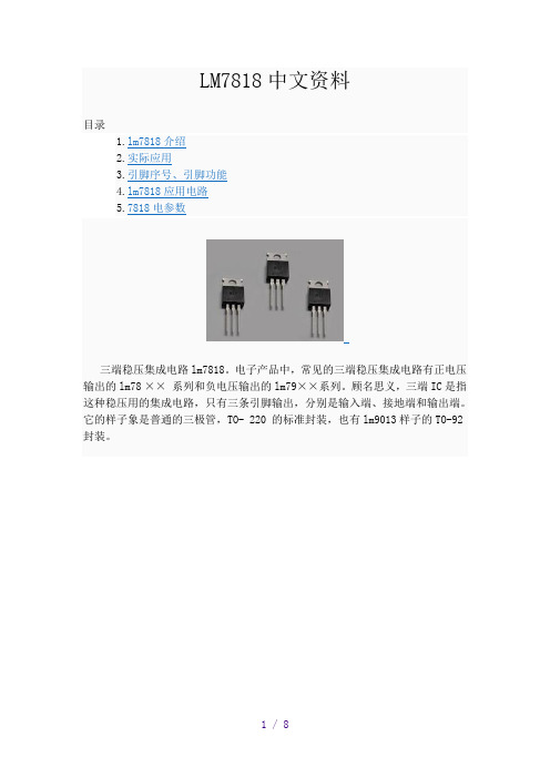
LM7818中文资料目录1.lm7818介绍2.实际应用3.引脚序号、引脚功能4.lm7818应用电路5.7818电参数三端稳压集成电路lm7818。
电子产品中,常见的三端稳压集成电路有正电压输出的lm78 ×× 系列和负电压输出的lm79××系列。
顾名思义,三端IC是指这种稳压用的集成电路,只有三条引脚输出,分别是输入端、接地端和输出端。
它的样子象是普通的三极管,TO- 220 的标准封装,也有lm9013样子的TO-92封装。
1.lm7818介绍用lm78/lm79系列三端稳压IC来组成稳压电源所需的外围元件极少,电路内部还有过流、过热及调整管的保护电路,使用起来可靠、方便,而且价格便宜。
该系列集成稳压IC型号中的lm78或lm79后面的数字代表该三端集成稳压电路的输出电压,如lm7806表示输出电压为正6V,lm7909表示输出电压为负9V。
因为三端固定集成稳压电路的使用方便,电子制作中经常采用。
最大输出电流1.5A,LM78XX系列输出电压分别为5V;6V;8V;9V;10V;12V;15V;18V;24V。
2.实际应用在实际应用中,应在三端集成稳压电路上安装足够大的散热器(当然小功率7818IC内部电路图.的条件下不用)。
当稳压管温度过高时,稳压性能将变差,甚至损坏。
当制作中需要一个能输出1.5A以上电流的稳压电源,通常采用几块三端稳压电路并联起来,使其最大输出电流为N个1.5A,但应用时需注意:并联使用的集成稳压电路应采用同一厂家、同一批号的产品,以保证参数的一致。
另外在输出电流上留有一定的余量,以避免个别集成稳压电路失效时导致其他电路的连锁烧毁。
在lm78 ** 、lm79 ** 系列三端稳压器中最常应用的是TO-220 和TO-202 两种封装。
这两种封装的图形以及引脚序号、引脚功能如附图所示。
图中的引脚号标注方法是按照引脚电位从高到底的顺序标注的。
L78L12中文资料

L78L00SERIESPOSITIVE VOLTAGE REGULATORS®November 1998s OUTPUT CURRENT UP TO 100mAsOUTPUT VOLTAGESOF 3.3;5;6;8;9;12;15;18;24Vs THERMAL OVERLOAD PROTECTION s SHORT CIRCUIT PROTECTIONsNO EXTERNAL COMPONENTS ARE REQUIREDsAVAILABLEIN EITHER ±5%(AC)OR ±10%(C)SELECTIONDESCRIPTIONThe L78L00series of three-terminal positive regulators employ internal current limiting and thermal shutdown,making them essentially indestructible.If adequate heatsink is provided,they can deliver up to 100mA output current.They are intended as fixed voltage regulators in a wide range of applications including local or on-card regulation for elimination of noise and distribution problems associated with single-point regulation.In addition,they can be used with power pass elements to make high-current voltage regulators.The L78L00series used as Zener diode/resistor combination replacement,offers an effectiveBLOCK DIAGRAMSO-8TO-92output impedance improvement of typically two orders of magnetude,along with lower quiescent current and lower noise.SOT-891/19ABSOLUTE MAXIMUM RATINGSymbol ParameterValue Unit V iDC Input VoltageV o =3.3V to 9V 30V V o =12V to 15V 35V V o =18V to 24V40V I o Output Current 100mA P tot Power DissipationInternally limited (*)T st g Storage Temperature Range-40to 150o C T opOperating Junction Temperature RangeFor L78L00C,L78L00AC For L78L00AB0to 125-40to 125o C oC(*)Our SO-8package used for Voltage Regulators is modified internally to have pins 2,3,6and 7electrically commoned to the die attach flag.This particular frame decreases the total thermal resistance of the package and increases its ability to dissipate power when an appropriate area of copper on the printed circuit board is available for heatsinking.The external dimensions are the same as for the standard SO-8TEST CIRCUITSTHERMAL DATASymbolParameterSO-8TO-92SOT-89UnitR thj-ca se R thj-amb Thermal Resistance Junction-case Max Thermal Resistance Junction-ambientMax2055(*)20012o C/W oC/W(*)Considering 6cm 2of copper Board heat-sinkL78L002/19CONNECTION DIAGRAM AND ORDERING NUMBERS(top view)ORDERING NUMBERSType SO-8TO-92SOT-89Output VoltageL78L33AC L78L33AB L78L05C L78L05AC L78L05AB L78L06C L78L06AC L78L06AB L78L08C L78L08AC L78L08AB L78L09C L78L09AC L78L09AB L78L12C L78L12AC L78L12AB L78L15C L78L15AC L78L15AB L78L18C L78L18AC L78L18AB L78L24C L78L24AC L78L24ABL78L33ACDL78L33ABDL78L05CDL78L05ACDL78L05ABDL78L06CDL78L06ACDL78L06ABDL78L08CDL78L08ACDL78L08ABDL78L09CDL78L09ACDL78L09ABDL78L12CDL78L12ACDL78L12ABDL78L15CDL78L15ACDL78L15ABDL78L18CDL78L18ACDL78L18ABDL78L24CDL78L24ACDL78L24ABDL78L33ACZL78L33ABZL78L05CZL78L05ACZL78L05ABZL78L06CZL78L06ACZL78L06ABZL78L08CZL78L08ACZL78L08ABZL78L09CZL78L09ACZL78L09ABZL78L12CZL78L12ACZL78L12ABZL78L15CZL78L15ACZL78L15ABZL78L18CZL78L18ACZL78L18ABZL78L24CZL78L24ACZL78L24ABZL78L33ACUL78L33ABUL78L05ACUL78L05ABUL78L06ACUL78L06ABUL78L08ACUL78L08ABUL78L09ACUL78L09ABUL78L12ACUL78L12ABUL78L15ACUL78L15ABUL78L18ACUL78L18ABUL78L24ACUL78L24ABU3.3V3.3V5V5V5V6V6V6V8V8V8V9V9V9V12V12V12V15V15V15V18V18V18V24V24V24VSO-8TO-92pin1=V OUTpin2=GNDpin3=V INBOTTOM VIEWSOT-89L78L003/19ELECTRICAL CHARACTERISTICS FOR L78L05(refer to the test circuits,T j=0to125o C,V i=10V,I o=40mA,C i=0.33µF,C o=0.1µF unless otherwise specified)Symbol Parameter Test Conditions Min.Typ.Max.Unit V o Output Voltage T j=25o C 4.65 5.4VV o Output Voltage I o=1to40mA V i=7to20VI o=1to70mA V i=10V 4.54.55.55.5VV∆V o Line Regulation V i=7to20V T j=25o CV i=8to20V T j=25o C 200150mVmV∆V o Load Regulation I o=1to100mA T j=25o CI o=1to40mA T j=25o C 6030mVmVI d Quiescent Current T j=25o CT j=125o C65.5mAmA∆I d Quiescent Current Change I o=1to40mA0.2mA ∆I d Quiescent Current Change V i=8to20V 1.5mA eN Output Noise Voltage B=10Hz to100KHz T j=25o C40µV SVR Supply Voltage Rejection I o=40mA f=120Hz T j=25o CV i=8to18V4049dB V d Dropout Voltage 1.7VELECTRICAL CHARACTERISTICS FOR L78L06(refer to the test circuits,T j=0to125o C,V i=12V,I o=40mA,C i=0.33µF,C o=0.1µF unless otherwise specified)Symbol Parameter Test Conditions Min.Typ.Max.Unit V o Output Voltage T j=25o C 5.526 6.48VV o Output Voltage I o=1to40mA V i=8.5to20VI o=1to70mA V i=12V 5.45.46.66.6VV∆V o Line Regulation V i=8.5to20V T j=25o CV i=9to20V T j=25o C 200150mVmV∆V o Load Regulation I o=1to100mA T j=25o CI o=1to40mA T j=25o C 6030mVmVI d Quiescent Current T j=25o CT j=125o C65.5mAmA∆I d Quiescent Current Change I o=1to40mA0.2mA ∆I d Quiescent Current Change V i=8to20V 1.5mA eN Output Noise Voltage B=10Hz to100KHz T j=25o C50µV SVR Supply Voltage Rejection I o=40mA f=120Hz T j=25o CV i=9to20V3846dB V d Dropout Voltage 1.7V L78L004/19ELECTRICAL CHARACTERISTICS FOR L78L08(refer to the test circuits,T j=0to125o C,V i=14V,I o=40mA,C i=0.33µF,C o=0.1µF unless otherwise specified)Symbol Parameter Test Conditions Min.Typ.Max.Unit V o Output Voltage T j=25o C7.3688.64VV o Output Voltage I o=1to40mA V i=10.5to23VI o=1to70mA V i=14V 7.27.28.88.8VV∆V o Line Regulation V i=10.5to23V T j=25o CV i=11to23V T j=25o C 200150mVmV∆V o Load Regulation I o=1to100mA T j=25o CI o=1to40mA T j=25o C 8040mVmVI d Quiescent Current T j=25o CT j=125o C65.5mAmA∆I d Quiescent Current Change I o=1to40mA0.2mA ∆I d Quiescent Current Change V i=11to23V 1.5mA eN Output Noise Voltage B=10Hz to100KHz T j=25o C60µV SVR Supply Voltage Rejection I o=40mA f=120Hz T j=25o CV i=12to23V3645dB V d Dropout Voltage 1.7VELECTRICAL CHARACTERISTICS FOR L78L09(refer to the test circuits,T j=0to125o C,V i=15V,I o=40mA,C i=0.33µF,C o=0.1µF unless otherwise specified)Symbol Parameter Test Conditions Min.Typ.Max.Unit V o Output Voltage T j=25o C8.2899.72VV o Output Voltage I o=1to40mA V i=11.5to23VI o=1to70mA V i=15V 8.18.19.99.9VV∆V o Line Regulation V i=11.5to23V T j=25o CV i=12to23V T j=25o C 250200mVmV∆V o Load Regulation I o=1to100mA T j=25o CI o=1to40mA T j=25o C 8040mVmVI d Quiescent Current T j=25o CT j=125o C65.5mAmA∆I d Quiescent Current Change I o=1to40mA0.2mA∆I d Quiescent Current Change V i=12to23V 1.5mA eN Output Noise Voltage B=10Hz to100KHz T j=25o C70µV SVR Supply Voltage Rejection I o=40mA f=120Hz T j=25o CV i=12to23V3644dBV d Dropout Voltage 1.7VL78L005/19ELECTRICAL CHARACTERISTICS FOR L78L12(refer to the test circuits,T j=0to125o C,V i=19V,I o=40mA,C i=0.33µF,C o=0.1µF unless otherwise specified)Symbol Parameter Test Conditions Min.Typ.Max.Unit V o Output Voltage T j=25o C11.11212.9VV o Output Voltage I o=1to40mA V i=14.5to27VI o=1to70mA V i=19V 10.810.813.213.2VV∆V o Line Regulation V i=14.5to27V T j=25o CV i=16to27V T j=25o C 250200mVmV∆V o Load Regulation I o=1to100mA T j=25o CI o=1to40mA T j=25o C 10050mVmVI d Quiescent Current T j=25o CT j=125o C 6.56mAmA∆I d Quiescent Current Change I o=1to40mA0.2mA ∆I d Quiescent Current Change V i=16to27V 1.5mA eN Output Noise Voltage B=10Hz to100KHz T j=25o C80µV SVR Supply Voltage Rejection I o=40mA f=120Hz T j=25o CV i=15to25V3642dB V d Dropout Voltage 1.7VELECTRICAL CHARACTERISTICS FOR L78L15(refer to the test circuits,T j=0to125o C,V i=23V,I o=40mA,C i=0.33µF,C o=0.1µF unless otherwise specified)Symbol Parameter Test Conditions Min.Typ.Max.Unit V o Output Voltage T j=25o C13.81516.2VV o Output Voltage I o=1to40mA V i=17.5to30VI o=1to70mA V i=23V 13.513.516.516.5VV∆V o Line Regulation V i=17.5to30V T j=25o CV i=20to30V T j=25o C 300250mVmV∆V o Load Regulation I o=1to100mA T j=25o CI o=1to40mA T j=25o C 15075mVmVI d Quiescent Current T j=25o CT j=125o C 6.56mAmA∆I d Quiescent Current Change I o=1to40mA0.2mA ∆I d Quiescent Current Change V i=20to30V 1.5mA eN Output Noise Voltage B=10Hz to100KHz T j=25o C90µV SVR Supply Voltage Rejection I o=40mA f=120Hz T j=25o CV i=18.5to28.5V3339dB V d Dropout Voltage 1.7V L78L006/19ELECTRICAL CHARACTERISTICS FOR L78L18(refer to the test circuits,T j=0to125o C,V i=27V,I o=40mA,C i=0.33µF,C o=0.1µF unless otherwise specified)Symbol Parameter Test Conditions Min.Typ.Max.Unit V o Output Voltage T j=25o C16.61819.4VV o Output Voltage I o=1to40mA V i=22to33VI o=1to70mA V i=27V 16.216.219.819.8VV∆V o Line Regulation V i=22to33V T j=25o CV i=22to33V T j=25o C 320270mVmV∆V o Load Regulation I o=1to100mA T j=25o CI o=1to40mA T j=25o C 17085mVmVI d Quiescent Current T j=25o CT j=125o C 6.56mAmA∆I d Quiescent Current Change I o=1to40mA0.2mA ∆I d Quiescent Current Change V i=23to33V 1.5mA eN Output Noise Voltage B=10Hz to100KHz T j=25o C120µV SVR Supply Voltage Rejection I o=40mA f=120Hz T j=25o CV i=23to33V3238dB V d Dropout Voltage 1.7VELECTRICAL CHARACTERISTICS FOR L78L24(refer to the test circuits,T j=0to125o C,V i=33V,I o=40mA,C i=0.33µF,C o=0.1µF unless otherwise specified)Symbol Parameter Test Conditions Min.Typ.Max.Unit V o Output Voltage T j=25o C22.12425.9VV o Output Voltage I o=1to40mA V i=27to38VI o=1to70mA V i=33V 21.621.626.426.4VV∆V o Line Regulation V i=27to38V T j=25o CV i=28to38V T j=25o C 350300mVmV∆V o Load Regulation I o=1to100mA T j=25o CI o=1to40mA T j=25o C 200100mVmVI d Quiescent Current T j=25o CT j=125o C 6.56mAmA∆I d Quiescent Current Change I o=1to40mA0.2mA∆I d Quiescent Current Change V i=28to38V 1.5mA eN Output Noise Voltage B=10Hz to100KHz T j=25o C200µV SVR Supply Voltage Rejection I o=40mA f=120Hz T j=25o CV i=29to35V3037dBV d Dropout Voltage 1.7VL78L007/19ELECTRICAL CHARACTERISTICS FOR L78L33AB AND L78L33AC(refer to the test circuits,V i=8.3V,I o=40mA,C i=0.33µF,C o=0.1µF,T j=0to125o C for L78L33AC,T j=-40to125o C for L78L33AB,unless otherwise specified)Symbol Parameter Test Conditions Min.Typ.Max.Unit V o Output Voltage T j=25o C 3.168 3.3 3.432VV o Output Voltage I o=1to40mA V i=5.3to20VI o=1to70mA V i=8.3V 3.1353.1353.4653.465VV∆V o Line Regulation V i=5.3to20V T j=25o CV i=6.3to20V T j=25o C 150100mVmV∆V o Load Regulation I o=1to100mA T j=25o CI o=1to40mA T j=25o C 6030mVmVI d Quiescent Current T j=25o CT j=125o C65.5mAmA∆I d Quiescent Current Change I o=1to40mA0.1mA ∆I d Quiescent Current Change V i=6.3to20V 1.5mA eN Output Noise Voltage B=10Hz to100KHz T j=25o C40µV SVR Supply Voltage Rejection I o=40mA f=120Hz T j=25o CV i=6.3to16.3V4149dB V d Dropout Voltage 1.7VELECTRICAL CHARACTERISTICS FOR L78L05AB AND L78L05AC(refer to the test circuits,V i=10V,I o=40mA,C i=0.33µF,C o=0.1µF,T j=0to125o C for L78L05AC,T j=-40to125o C for L78L05AB,unless otherwise specified)Symbol Parameter Test Conditions Min.Typ.Max.Unit V o Output Voltage T j=25o C 4.85 5.2VV o Output Voltage I o=1to40mA V i=7to20VI o=1to70mA V i=10V 4.754.755.255.25VV∆V o Line Regulation V i=7to20V T j=25o CV i=8to20V T j=25o C 150100mVmV∆V o Load Regulation I o=1to100mA T j=25o CI o=1to40mA T j=25o C 6030mVmVI d Quiescent Current T j=25o CT j=125o C65.5mAmA∆I d Quiescent Current Change I o=1to40mA0.1mA ∆I d Quiescent Current Change V i=8to20V 1.5mA eN Output Noise Voltage B=10Hz to100KHz T j=25o C40µV SVR Supply Voltage Rejection I o=40mA f=120Hz T j=25o CV i=8to18V4149dB V d Dropout Voltage 1.7V L78L008/19ELECTRICAL CHARACTERISTICS FOR L78L06AB AND L78L06AC(refer to the test circuits,V i=12V,I o=40mA,C i=0.33µF,C o=0.1µF,T j=0to125o C for L78L06AC,T j=-40to125o C for L78L06AB,unless otherwise specified)Symbol Parameter Test Conditions Min.Typ.Max.Unit V o Output Voltage T j=25o C 5.766 6.24VV o Output Voltage I o=1to40mA V i=8.5to20VI o=1to70mA V i=12V 5.75.76.36.3VV∆V o Line Regulation V i=8.5to20V T j=25o CV i=9to20V T j=25o C 150100mVmV∆V o Load Regulation I o=1to100mA T j=25o CI o=1to40mA T j=25o C 6030mVmVI d Quiescent Current T j=25o CT j=125o C65.5mAmA∆I d Quiescent Current Change I o=1to40mA0.1mA ∆I d Quiescent Current Change V i=9to20V 1.5mA eN Output Noise Voltage B=10Hz to100KHz T j=25o C50µV SVR Supply Voltage Rejection I o=40mA f=120Hz T j=25o CV i=9to20V3946dB V d Dropout Voltage 1.7VELECTRICAL CHARACTERISTICS FOR L78L08AB AND L78L08AC(refer to the test circuits,V i=14V,I o=40mA,C i=0.33µF,C o=0.1µF,T j=0to125o C for L78L08AC,T j=-40to125o C for L78L08AB,unless otherwise specified)Symbol Parameter Test Conditions Min.Typ.Max.Unit V o Output Voltage T j=25o C7.6888.32VV o Output Voltage I o=1to40mA V i=10.5to23VI o=1to70mA V i=14V 7.67.68.48.4VV∆V o Line Regulation V i=10.5to23V T j=25o CV i=11to23V T j=25o C 175125mVmV∆V o Load Regulation I o=1to100mA T j=25o CI o=1to40mA T j=25o C 8040mVmVI d Quiescent Current T j=25o CT j=125o C65.5mAmA∆I d Quiescent Current Change I o=1to40mA0.1mA∆I d Quiescent Current Change V i=11to23V 1.5mA eN Output Noise Voltage B=10Hz to100KHz T j=25o C60µV SVR Supply Voltage Rejection I o=40mA f=120Hz T j=25o CV i=12to23V3745dBV d Dropout Voltage 1.7VL78L009/19ELECTRICAL CHARACTERISTICS FOR L78L09AB AND L78L09AC(refer to the test circuits,V i=15V,I o=40mA,C i=0.33µF,C o=0.1µF,T j=0to125o C for L78L09AC,T j=-40to125o C for L78L09AB,unless otherwise specified)Symbol Parameter Test Conditions Min.Typ.Max.Unit V o Output Voltage T j=25o C8.6499.36VV o Output Voltage I o=1to40mA V i=11.5to23VI o=1to70mA V i=15V 8.558.559.459.45VV∆V o Line Regulation V i=11.5to23V T j=25o CV i=12to23V T j=25o C 225150mVmV∆V o Load Regulation I o=1to100mA T j=25o CI o=1to40mA T j=25o C 8040mVmVI d Quiescent Current T j=25o CT j=125o C65.5mAmA∆I d Quiescent Current Change I o=1to40mA0.1mA ∆I d Quiescent Current Change V i=12to23V 1.5mA eN Output Noise Voltage B=10Hz to100KHz T j=25o C70µV SVR Supply Voltage Rejection I o=40mA f=120Hz T j=25o CV i=12to23V3744dB V d Dropout Voltage 1.7VELECTRICAL CHARACTERISTICS FOR L78L12AB AND L78L12AC(refer to the test circuits,V i=19V,I o=40mA,C i=0.33µF,C o=0.1µF,T j=0to125o C for L78L12AC,T j=-40to125o C for L78L12AB,unless otherwise specified)Symbol Parameter Test Conditions Min.Typ.Max.Unit V o Output Voltage T j=25o C11.51212.5VV o Output Voltage I o=1to40mA V i=14.5to27VI o=1to70mA V i=19V 11.411.412.612.6VV∆V o Line Regulation V i=14.5to27V T j=25o CV i=16to27V T j=25o C 250200mVmV∆V o Load Regulation I o=1to100mA T j=25o CI o=1to40mA T j=25o C 10050mVmVI d Quiescent Current T j=25o CT j=125o C 6.56mAmA∆I d Quiescent Current Change I o=1to40mA0.1mA ∆I d Quiescent Current Change V i=16to27V 1.5mA eN Output Noise Voltage B=10Hz to100KHz T j=25o C80µV SVR Supply Voltage Rejection I o=40mA f=120Hz T j=25o CV i=15to25V3742dB V d Dropout Voltage 1.7V L78L0010/19ELECTRICAL CHARACTERISTICS FOR L78L15AB AND L78L15AC(refer to the test circuits,V i=23V,I o=40mA,C i=0.33µF,C o=0.1µF,T j=0to125o C for L78L15AC,T j=-40to125o C for L78L15AB,unless otherwise specified)Symbol Parameter Test Conditions Min.Typ.Max.Unit V o Output Voltage T j=25o C14.41515.6VV o Output Voltage I o=1to40mA V i=17.5to30VI o=1to70mA V i=23V 14.2514.2515.7515.75VV∆V o Line Regulation V i=17.5to30V T j=25o CV i=20to30V T j=25o C 300250mVmV∆V o Load Regulation I o=1to100mA T j=25o CI o=1to40mA T j=25o C 15075mVmVI d Quiescent Current T j=25o CT j=125o C 6.56mAmA∆I d Quiescent Current Change I o=1to40mA0.1mA ∆I d Quiescent Current Change V i=20to30V 1.5mA eN Output Noise Voltage B=10Hz to100KHz T j=25o C90µV SVR Supply Voltage Rejection I o=40mA f=120Hz T j=25o CV i=18.5to28.5V3439dB V d Dropout Voltage 1.7VELECTRICAL CHARACTERISTICS FOR L78L18AB AND L78L18AC(refer to the test circuits,V i=27V,I o=40mA,C i=0.33µF,C o=0.1µF,T j=0to125o C for L78L18AC,T j=-40to125o C for L78L18AB,unless otherwise specified)Symbol Parameter Test Conditions Min.Typ.Max.Unit V o Output Voltage T j=25o C17.31818.7VV o Output Voltage I o=1to40mA V i=22to33VI o=1to70mA V i=27V 17.117.118.918.9VV∆V o Line Regulation V i=22to33V T j=25o CV i=22to33V T j=25o C 320270mVmV∆V o Load Regulation I o=1to100mA T j=25o CI o=1to40mA T j=25o C 17085mVmVI d Quiescent Current T j=25o CT j=125o C 6.56mAmA∆I d Quiescent Current Change I o=1to40mA0.1mA∆I d Quiescent Current Change V i=23to33V 1.5mA eN Output Noise Voltage B=10Hz to100KHz T j=25o C120µV SVR Supply Voltage Rejection I o=40mA f=120Hz T j=25o CV i=23to33V3338dBV d Dropout Voltage 1.7V11/19ELECTRICAL CHARACTERISTICS FOR L78L24AB AND L78L24AC(refer to the test circuits,V i=33V,I o=40mA,C i=0.33µF,C o=0.1µF,T j=0to125o C for L78L24AC,T j=-40to125o C for L78L24AB,unless otherwise specified)Symbol Parameter Test Conditions Min.Typ.Max.Unit V o Output Voltage T j=25o C232425VV o Output Voltage I o=1to40mA V i=27to38VI o=1to70mA V i=33V 22.822.825.225.2VV∆V o Line Regulation V i=27to38V T j=25o CV i=28to38V T j=25o C 350300mVmV∆V o Load Regulation I o=1to100mA T j=25o CI o=1to40mA T j=25o C 200100mVmVI d Quiescent Current T j=25o CT j=125o C 6.56mAmA∆I d Quiescent Current Change I o=1to40mA0.1mA ∆I d Quiescent Current Change V i=28to38V 1.5mA eN Output Noise Voltage B=10Hz to100KHz T j=25o C200µV SVR Supply Voltage Rejection I o=40mA f=120Hz T j=25o CV i=29to35V3137dB V d Dropout Voltage 1.7V12/19Figure3:L78L05/12/24Thermal Shutdown.Figure4:L78L05/12Quiescent Current vsOutput CurrentFigure5:L78L05Quiescent Current vs Input Voltage.Figure6:L78L05/12/24Output Characteristics.Figure1:L78L05/12Output Voltage vs AmbientTemperatureFigure2:L78L05/12/24Load Characteristics.13/19Figure7:L78L05/12/24Ripple Rejection.Figure8:L78L05Dropout Characteristics. Figure9:L78L00Series Short Circuit OutputCurrent.TYPICAL APPLICATIONS:Figure10:High Output Current Short Circuit Protected14/19Figure11:Output Boost Circuit.Figure12:Current Regulator.Figure13:Adjustable Output Regulator15/19SO-8MECHANICAL DATAmm inch DIM.MIN.TYP.MAX.MIN.TYP.MAX.A 1.750.068a10.10.250.0030.009 a2 1.650.064 a30.650.850.0250.033 b0.350.480.0130.018 b10.190.250.0070.010 C0.250.50.0100.019 c145(typ.)D 4.8 5.00.1880.196E 5.8 6.20.2280.244e 1.270.050e3 3.810.150F 3.8 4.00.140.157L0.4 1.270.0150.050 M0.60.023 S8(max.)0016023 16/19SOT-89MECHANICAL DATAmm milsDIM.MIN.TYP.MAX.MIN.TYP.MAX.A 1.4 1.655.163.0B0.440.5617.322.0B10.360.4814.218.9C0.350.4413.817.3C10.350.4413.817.3D 4.4 4.6173.2181.1D1 1.62 1.8363.872.0E 2.29 2.690.2102.4e 1.42 1.5755.961.8e1 2.92 3.07115.0120.9H 3.94 4.25155.1167.3L0.89 1.235.047.2P025H17/19TO-92MECHANICAL DATAmm inch DIM.MIN.TYP.MAX.MIN.TYP.MAX.A 4.58 5.330.1800.210B 4.45 5.20.1750.204C 3.2 4.20.1260.165D12.70.500E 1.270.050F0.40.510.0160.020 G0.350.1418/19Information furnished is believed to be accurate and reliable.However,STMicroelectronics assumes no responsibility for the consequence s of use of such information nor for any infringement of patents or other rights of third parties which may result from its use.No license is granted by implication or otherwise under any patent or patent rights of STMicroelectronics.Specification mentioned in this publication are subject to change without notice.This publication supersedes and replaces all information previously supplied.STMicroelectronics products are not authorized for use as critical components in life support devices or systems without express written approval of STMicroelectronics.The ST logo is a registered trademark of STMicroelectronics©1998STMicroelectronics–Printed in Italy–All Rights ReservedSTMicroelectronics GROUP OF COMPANIESAustralia-Brazil-Canada-China-France-Germany-Italy-Japan-Korea-Malaysia-Malta-Mexico-Morocco-The Netherlands-Singapore-Spain-Sweden-Switzerland-Taiwan-Thailand-United Kingdom-U.S.A..19/19。
LM78L12中文资料
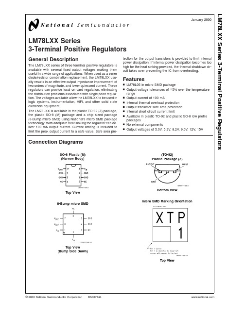
LM78LXX Series3-Terminal Positive RegulatorsGeneral DescriptionThe LM78LXX series of three terminal positive regulators isavailable with several fixed output voltages making themuseful in a wide range of applications.When used as a zenerdiode/resistor combination replacement,the LM78LXX usu-ally results in an effective output impedance improvement oftwo orders of magnitude,and lower quiescent current.Theseregulators can provide local on card regulation,eliminatingthe distribution problems associated with single point regula-tion.The voltages available allow the LM78LXX to be used inlogic systems,instrumentation,HiFi,and other solid stateelectronic equipment.The LM78LXX is available in the plastic TO-92(Z)package,the plastic SO-8(M)package and a chip sized package(8-Bump micro SMD)using National’s micro SMD packagetechnology.With adequate heat sinking the regulator can de-liver100mA output current.Current limiting is included tolimit the peak output current to a safe value.Safe area pro-tection for the output transistors is provided to limit internalpower dissipation.If internal power dissipation becomes toohigh for the heat sinking provided,the thermal shutdown cir-cuit takes over preventing the IC from overheating.Featuresn LM78L05in micro SMD packagen Output voltage tolerances of±5%over the temperaturerangen Output current of100mAn Internal thermal overload protectionn Output transistor safe area protectionn Internal short circuit current limitn Available in plastic TO-92and plastic SO-8low profilepackagesn No external componentsn Output voltages of5.0V,6.2V,8.2V,9.0V,12V,15V Connection DiagramsSO-8Plastic(M)(Narrow Body)DS007744-2Top View8-Bump micro SMDDS007744-24Top View(Bump Side Down)(TO-92)Plastic Package(Z)January2000LM78LXXSeries3-TerminalPositiveRegulators ©2000National Semiconductor Corporation Absolute Maximum Ratings (Note 1)If Military/Aerospace specified devices are required,please contact the National Semiconductor Sales Office/Distributors for availability and specifications.Power Dissipation (Note 5)Internally LimitedInput Voltage35VStorage Temperature−65˚C to +150˚COperating Junction Temperature SO-80˚C to 125˚C micro SMD−40˚C to 85˚C Soldering InformationInfrared or Convection (20sec.)235˚CWave Soldering (10sec.)260˚C (lead time)ESD Susceptibility (Note 2)1kVLM78LXX Electrical CharacteristicsLimits in standard typeface are for T J =25˚C,Bold typeface ap-plies over 0˚C to 125˚C for SO-8package and −40˚C to 85˚C for micro SMD package.Limits are guaranteed by produc-tion testing or correlation techniques using standard Statistical Quality Control (SQC)methods.Unless otherwise specified:I O =40mA,C I =0.33µF,C O =0.1µF.LM78L05Unless otherwise specified,V IN =10V Symbol ParameterConditionsMin Typ Max UnitsV OOutput Voltage4.855.2V 7V ≤V IN ≤20V 1mA ≤I O ≤40mA (Note 3)4.755.251mA ≤I O ≤70mA (Note 3)4.755.25∆V O Line Regulation 7V ≤V IN ≤20V 1875mV 8V ≤V IN ≤20V 1054∆V O Load Regulation 1mA ≤I O ≤100mA 20601mA ≤I O ≤40mA530I Q Quiescent Current 35mA ∆I Q Quiescent Current Change 8V ≤V IN ≤20V 1.01mA ≤I O ≤40mA 0.1V nOutput Noise Voltage f =10Hz to 100kHz (Note 4)40µV Ripple Rejectionf =120Hz8V ≤V IN ≤16V 4762dB I PKPeak Output Current140mALM78L62AC(Continued)Unless otherwise specified,V IN =12VSymbol ParameterConditionsMinTyp Max UnitsI Q Quiescent Current 25.5mA ∆I Q Quiescent Current Change 8V ≤V IN ≤20V 1.51mA ≤I O ≤40mA 0.1V nOutput Noise Voltage f =10Hz to 100kHz (Note 4)50µV Ripple Rejectionf =120Hz10V ≤V IN ≤20V4046dB I PKPeak Output Current140mA Average Output Voltage TempcoI O =5mA−0.8mV/˚C V IN (Min)Minimum Value of Input VoltageRequired to Maintain Line Regulation9.9VLM78L09ACUnless otherwise specified,V IN =15V Symbol ParameterConditionsMin Typ Max UnitsV OOutput Voltage8.649.09.36V 11.5V ≤V IN ≤24V 1mA ≤I O ≤40mA (Note 3)8.559.451mA ≤I O ≤70mA (Note 3)8.559.45LM78LXX Series3LM78L09AC(Continued)Unless otherwise specified,V IN =15VSymbol ParameterConditions MinTyp Max Units∆V O Line Regulation 11.5V ≤V IN ≤24V 100200mV 13V ≤V IN ≤24V 90150∆V O Load Regulation 1mA ≤I O ≤100mA 20901mA ≤I O ≤40mA1045I Q Quiescent Current 25.5mA ∆I Q Quiescent Current Change 11.5V ≤V IN ≤24V 1.51mA ≤I O ≤40mA0.1V nOutput Noise Voltage 70µV Ripple Rejectionf =120Hz15V ≤V IN ≤25V3844dB I PKPeak Output Current140mA Average Output Voltage TempcoI O =5mA−1.0mV/˚C V IN (Min)Minimum Value of Input VoltageRequired to Maintain Line Regulation13.714.5VL M 78L X X S e r i e s 4LM78L15ACUnless otherwise specified,V IN =23V Symbol ParameterConditionsMin Typ Max UnitsV OOutput Voltage14.415.015.6V 17.5V ≤V IN ≤30V 1mA ≤I O ≤40mA (Note 3)14.2515.751mA ≤I O ≤70mA (Note 3)14.2515.75∆V O Line Regulation 17.5V ≤V IN ≤30V 37250mV 20V ≤V IN ≤30V 25140∆V O Load Regulation 1mA ≤I O ≤100mA 351501mA ≤I O ≤40mA1275I QQuiescent Current 35mA ∆I QQuiescent Current Change 20V ≤V IN ≤30V 11mA ≤I O ≤40mA0.1V nOutput Noise Voltage 90µV Ripple Rejectionf =120Hz18.5V ≤V IN ≤28.5V3751dB I PKPeak Output Current140mATypical Performance CharacteristicsMaximum Average Power Dissipation (Z Package)DS007744-14Peak Output CurrentDS007744-16Dropout VoltageDS007744-17Ripple Rejection DS007744-18Output Impedance DS007744-19Quiescent CurrentDS007744-20Quiescent CurrentDS007744-21L M 78L X X S e r i e s 6Equivalent CircuitTypical ApplicationsLM78LXXDS007744-7Fixed Output RegulatorDS007744-8*Required if the regulator is located more than 3"from the power supply filter.**See (Note 4)in the electrical characteristics table.LM78LXX Series7Typical Applications(Continued)Adjustable Output RegulatorDS007744-9V OUT=5V+(5V/R1+I Q)R25V/R1>3I Q,load regulation(L r)≈[(R1+R2)/R1](L r of LM78L05)Current RegulatorDS007744-10I OUT=(V OUT/R1)+I Q>I Q=1.5mA over line and load changes5V,500mA Regulator with Short Circuit ProtectionDS007744-11*Solid tantalum.**Heat sink Q1.***Optional:Improves ripple rejection and transient response.Load Regulation:0.6%0≤I L≤250mA pulsed with t ON=50ms.±15V,100mA Dual Power Supply8Typical Applications(Continued)Variable Output Regulator0.5V-18VDS007744-13*Solid tantalum.V OUT=V G+5V,R1=(−V IN/I Q LM78L05)V OUT=5V(R2/R4)for(R2+R3)=(R4+R5)A0.5V output will correspond to(R2/R4)=0.1(R3/R4)=0.9LM78LXXSeries 9Physical Dimensionsinches (millimeters)unless otherwise notedNOTES:UNLESS OTHERWISE SPECIFIED 1.EPOXY COATING2.63Sn/37Pb EUTECTIC BUMP3.RECOMMEND NON-SOLDER MASK DEFINED LANDING PAD.4.PIN 1IS ESTABLISHED BY LOWER LEFT CORNER WITH RESPECT TO TEXT ORIENTATION.REMAINING PINS ARE NUMBERED COUNTERCLOCKWISE.5.XXX IN DRAWING NUMBER REPRESENTS PACKAGE SIZE VARIATION WHERE X 1IS PACKAGE WIDTH,X 2IS PACK-AGE LENGTH AND X 3IS PACKAGE HEIGHT.6.REFERENCE JEDEC REGISTRATION MO-211,VARIATION BC.8-Bump micro SMDOrder Number LM78L05IBP or LM78L05IBPXNS Package Number BPA08AAA X 1=1.285X 2=1.285X 3=0.7L M 78L X X S e r i e s 10Physical Dimensionsinches (millimeters)unless otherwise noted (Continued)S.O.Package (M)Order Number LM78L05ACM,LM78L12ACM or LM78L15ACMNS Package Number M08AMolded Offset TO-92(Z)Order Number LM78L05ACZ,LM78L09ACZ,LM78L12ACZ,LM78L15ACZ,LM78L62ACZ or LM78L82ACZNS Package Number Z03ALM78LXX Series11NotesLIFE SUPPORT POLICYNATIONAL’S PRODUCTS ARE NOT AUTHORIZED FOR USE AS CRITICAL COMPONENTS IN LIFE SUPPORT DEVICES OR SYSTEMS WITHOUT THE EXPRESS WRITTEN APPROVAL OF THE PRESIDENT AND GENERAL COUNSEL OF NATIONAL SEMICONDUCTOR CORPORATION.As used herein:1.Life support devices or systems are devices or systems which,(a)are intended for surgical implant into the body,or (b)support or sustain life,and whose failure to perform when properly used in accordance with instructions for use provided in the labeling,can be reasonably expected to result in a significant injury to the user.2.A critical component is any component of a life support device or system whose failure to perform can be reasonably expected to cause the failure of the life support device or system,or to affect its safety or effectiveness.National Semiconductor Corporation AmericasTel:1-800-272-9959Fax:1-800-737-7018Email:support@National Semiconductor EuropeFax:+49(0)180-5308586Email:europe.support@Deutsch Tel:+49(0)180-5308585English Tel:+49(0)180-5327832Français Tel:+49(0)180-5329358Italiano Tel:+49(0)180-5341680National Semiconductor Asia Pacific Customer Response Group Tel:65-2544466Fax:65-2504466Email:sea.support@National Semiconductor Japan Ltd.Tel:81-3-5639-7560Fax:81-3-5639-7507L M 78L X X S e r i e s 3-T e r m i n a l P o s i t i v e R e g u l a t o r sNational does not assume any responsibility for use of any circuitry described,no circuit patent licenses are implied and National reserves the right at any time without notice to change said circuitry and specifications.。
DMP78中文说明书1.1

向日葵“无碟王”车载多媒体影音播放器使用说明书(型号:DMP-780)在连接、操作或是调整本产品之前,请仔细阅读下面的介绍。
请保留本手册以备将来参考。
目录1. 功能特点1.1主要特征 (2)2. 主要功能描述2.1面板定义说明 (3)2.2功能菜单说明 (4)3. 基本功能操作3.1状态切换 (5)3.2开机播放 (5)3.3快速向前/向后播放 (5)3.5选择曲目 (5)3.6选择字幕语言 (5)3.7选择音频通道 (5)3.8显示状态 (5)3.9音量控制 (6)3.10高音、低音、左右平衡和响度 (6)3.11播放WMA,MP3等格式文件 (6)4. 收音功能操作4.1选择收音功能 (8)4.2全局搜索自动存储电台 (8)4.3自动搜索电台 (8)4.4手动搜索电台 (8)4.5收听已存储的电台 (8)4.6音量和音效等控制 (8)4.7立体声单声道切换 (8)5. 外接输入操作5.1选择外接输入功能 (9)5.2音量、静音和音效控制 (9)6. 常见问题提示 (10)7. 规格参数 (11)8. 附件 (12)9. 连接图 (12)功能特点1.1主要特征:1 本播放器为标准IN-DASH 尺寸;2 本播放器无机芯,可通过USB接口接U盘,移动硬盘等,另支持SD卡;(可播放CD, MP3,WMA,MPEG-2,MPEG-4等文件格式)3 带调频/调幅收音机,FM频率范围:87.5~108MHz;AM频率范围:522~1620KHz;4 断电记忆功能:当电源突然断掉时,重新开机,机器将从上次断电前那一曲/点播放,而不是从头播放;5 2通道模拟音频输入;6 一路视频输入(可外接倒车摄像头)7 前面板上带AUX IN输入插孔;8 FM可预存30个台,AM可预存12个台;9 2.5寸TFT屏显示;9 阻抗4 Ω时,最大输出4 x 45 W ;10 无机芯设计,有效解决防尘与散热方面的问题;11 全功能面板操作,方便快捷;注意事项:使用时,请在电脑上用FAT32或FAT的格式格式化硬盘/U盘或SD卡,本机暂不支持NTFS格式的文件系统!且硬盘不要分成几个盘区,多分区硬盘可能会导致部分文件无法读到的现象!主要功能描述2.1面板定义说明:1. 上一曲键(在进入多功能菜单时为功能键)2. 播放快退键(在进入多功能菜单时为功能键)3. 播放/暂停键(在进入多功能菜单时为功能键)4. 状态切换键(在同时接上SD卡与USB设备时,按住此键可以在SD卡与USB设备之间切换)5. 下一曲键(在进入多功能菜单时为功能键)6. 播放快进键 (在进入多功能菜单时为功能键)7. 停止键(在进入多功能菜单时为功能键)8. BAND键(在播放状态时为多功能菜单键)在FM/AM状态时为选择波段;在播放USB/SD状态时为多功能菜单选择键,播放时按该键进入数字选曲菜单;再次按该键进入播放设置菜单。