(2004)High-rate flame synthesis of vertically aligned carbon nanotubes using electric field control
超净工作台说明书

产品说明书超净工作台的优点是操作方便自如,比较舒适,工作效率高,预备时间短,开机30分钟以上即可操作,基本上可随时使用。
在工厂化生产中,接种工作量很大,需要经常长久地工作时,超净台是很理想的设备。
超净工作台由三相电机作鼓风动力,功率145~260W左右,将空气通过由特制的微孔泡沫塑料片层叠合组成的“超级滤清器”后吹送出来,形成连续不断的无尘无菌的超净空气层流,即所谓“高效的特殊空气”,它除去了大于0.3μm的尘埃、真菌和细菌孢子等等。
超净空气的流速为24~30m/min,这已足够防止附近空气可能袭扰而引起的污染,这样的流速也不会妨碍采用酒精灯或本生灯对器械等的灼烧消毒。
工作人员就在这样的无菌条件下操作,保持无菌材料在转移接种过程中不受污染。
但是万一操作中途遇到停电,暴露在未过滤空气中的材料便难以幸免污染。
这时应迅速结束工作,并在瓶上作出记号,内中的材料如处于增殖阶段,则以后不再用作增殖而转入生根培养。
如为一般性生产材料,因极其丰富也可弃去。
如处于生根过程,则可留待以后种植用。
超净台电源多采用三相四线制,其中有一零线,连通机器外壳,应接牢在地线上,另外三线都是相线,工作电压是380V。
三线接入电路中有一定的顺序,如线头接错了,风机会反转,这时声音正常或稍不正常,超净台正面无风(可用酒精灯火焰观察动静,不宜久试),应及时切断电源,只要将其中任何两相的线头交换一下位置再接上,就可解决。
三相线如只接入两相,或三相中有一相接触不良,则机器声音很不正常,应立即切断电源仔细检修,否则会烧毁电机。
这些常识应在开始使用超净台时就向工作人员讲解清楚,免除不应造成的事故与损失。
超净工作台进风口在背面或正面的下方,金属网罩内有一普通泡沫塑料片或无纺布,用以阻拦大颗粒尘埃,应常检查、拆洗,如发现泡沫塑料老化,要及时更换。
除进风口以外,如有漏气孔隙,应当堵严,如贴胶布,塞棉花,贴胶水纸等。
工作台正面的金属网罩内是超级滤清器,超级滤清器也可更换,如因使用年久,尘粒堵塞,风速减小,不能保证无菌操作时,则可换上新的。
镁铝合金直接燃烧法合成AlN晶体镁铝合金直接燃烧法合成AlN晶体

镁铝合金直接燃烧法合成AlN晶体镁铝合金直接燃烧法合成AlN晶体谢晓;隋颖;黄晓昱;朱晨光【摘要】以球形镁铝合金(Al12Mg17)颗粒为原料,在空气中直接燃烧合成氮化铝(AlN)晶体.实验样品堆积在直径为1 cm的区域内,使用乙烷火焰点燃.使用高速摄像仪记录燃烧合成过程.借助XRD和SEM对原料和产物的组成及结构进行分析,并使用TG-DSC分析合金的热力学性质.结果表明:镁铝合金中的铝可以全部转化为AlN 晶体.合金的点火温度约为494.4℃,一旦点燃,不需要外界热源的持续加热,样品可持续燃烧.燃烧开始后,合金颗粒中镁快速汽化,与空气中氧发生优先反应,并耗掉颗粒周围的氧气,使氮气进入液态铝表层,生成氮化铝.燃烧产物有明显分层,检测结果表明上层产物为白色氧化镁,下层产物为黑色氮化铝晶体.合成过程中,镁对氮化铝的形成起着积极的促进作用.【期刊名称】《无机材料学报》【年(卷),期】2019(034)004【总页数】5页(P439-443)【关键词】AlN;镁铝合金;燃烧【作者】谢晓;隋颖;黄晓昱;朱晨光【作者单位】南京理工大学化工学院,南京 210094;南京理工大学化工学院,南京210094;南京理工大学化工学院,南京 210094;南京理工大学化工学院,南京210094【正文语种】中文【中图分类】TQ174氮化铝具有优良的性能,被广泛应用在半导体,陶瓷以及光电等领域[1-3]。
传统合成氮化铝的方法主要包括碳热还原法、直接氮化法和自蔓延高温合成法等[4]。
对于直接氮化法和自蔓延高温合成法,由于氮气渗透能垒的存在,反应往往需要在高压下进行。
并且,反应对氮化温度有着严格的要求[5-7]。
对于碳热还原法[8],虽然能获得较为纯净的氮化铝,但是其还原温度一般在1000 ℃以上,并且由于在合成过程中使用了过量的碳粉,碳热还原法制得的氮化铝还需进行脱碳处理,合成耗时且工艺复杂,对设备要求较高。
近几年的研究发现,当纳米铝粉在空气中燃烧时,产物中会含有大量的氮化铝。
高能量分辨率X射线光谱仪基于块状漂移检测器的设计说明书

A High Energy Resolution X-ray Spectrometer using SDDCHEN Er Lei 1, 2, a , FENG Chang Qing 1, 2, b *,YE Chun Feng 1, 2, and LIU Shu Bin 1, 21Modern Physics Department, University of Science and Technology of China2The State Key Laboratory of Particle Detection and Electronics, USTCa ****************,b ***************.cn*Correspondingauthor.Tel.**************.E-mailaddress:***************.cn.Keywords: Spectrometer, X-ray, Silicon Drift Detector, high energy resolution, FWHM.Abstract. A high energy resolution X-ray spectrometer based on Silicon Drift Detector is described in this paper. The spectrometer consists of the SDD detector module, the analog electronics for shaping and filtering and the digital electronics for peak detection and data transfer. The system can working at room temperature as a thermo electric cooler (Peltier Element) is integrated into the SDD chip. The dynamic range is about 1 keV to 10 keV. Test results indicated high energy resolution Full Width at Half Maximum (FWHM), which is better than 160 eV @ 5.9 keV with the incoming photon of radioisotopes (55Fe).IntroductionThe radiation of X-rays are widely used in many fields (such as airport security, X-ray astronomy, X-ray medical, X-ray crystallography, X-ray microscopic and so on) based on its properties [1]. X-rays with photon energies above 5 - 10 keV are called hard X-rays, while those with lower energy are called soft X-rays. A high energy resolution of Soft X-ray Detection (SXD) system is very necessary anduseful in scientific experiments and to explor the origin of the universe. Photon energy (keV)D e t e c t i o n e f f i c i e n c y (%)Fig. 1 SDD detector and its absolution efficiencySilicon Drift Detectors (SDD) are the state-of-the-art X-ray detectors based on silicon substrates. As shown in Fig. 1 is the used detector KETEK VITUS SDD H30 [2] and its absolution efficiency curve (about 70% at 1 keV and 98% at 10 keV), while the detector have 30 mm 2 active area with 8 µm Be window. An incoming photon will generate a number of electrons and holes dependent on its energy.A followed readout electronics based on the SDD will be discribed in the following sections. Joint International Mechanical, Electronic and Information Technology Conference (JIMET 2015)Structure of the readout electronicsA m p l i t u d e (V )A m p l i t u d e (m V )As shown in Fig. 2, is the structure of the readout electronics. The SDD detector is surpported bythe High Voltage Module and Temperature Controller to guarantee a good working environment, while the statues of the voltage and temperature were monitored by the Field Programmable Gate Array (FPGA) simultaneously. The output of the SDD is buffered by a low-noise & high-gain Pre-Amp, which is a voltage step well between ± 2 V because of the reset signal. The output of the Pre-Amp is followed by the CR-RC 2 [3] filter and shaper, after then the quasi-Gaussian output is fed to the Peak Hold module and then be digitalized by a 14-bit Analog to Digital Converter (ADC) (3 MHz sample rate). The digitized results is buffred and packaged in the FPGA, then be readout to remote PC. Detailes will be listed bellow.Silicon Drift DetectorU BACK(-65V)U OR (-130V)U IR(-20V)GND X-rayEntrance windowAnode FETC FBAs shown in Fig. 3 is the schematic of the SDD chip. The anode of the SDD is connected to a Field Effect Transistor (FET) and Feed Back Capacitance (C FB ) which forms the first part of a Charge Sensitive Amplifier (CSA). A certain rise time is dependent on the location of interaction of the X-ray with the SDD chip, while a certain amplitude is dependent on the energy of the incoming photon. SDDs require High Voltages Power Supply (low noise stabilized, U OR ‘-130V ’, U IR ‘-25V ’, U BACK ‘-65V ’,), Preamplifier Module (ultra-low-noise, charge-sensitive, ramped reset type, high-gain) andTemperature Controller Module (Peltier Element based thermo electric cooler) to guarantee a good working enviroment, meanwhile it is necessary to read out the temperature sensor of the SDD. Peak-Hold moduleOne kernel part of the readout electronics is the Peak Hold method, which combine with Analog to Digital Converter (ADC) for peak detection. The peak of the analog quasi-Gaussian output is detected and held by the Peak Hold module, then be injected to ADC for digitization. A high performance peak-hold chip (PH300) was chosen, which was designed for satellite instrumentation (equally useful in laboratory and commercial applications for its stability and characteristics).Detected peakFig. 4 The Function and Timing diagram of PH300 [4]PH300 is a peak-hold device, to track an analog input and keep the maximum amplitude as a peak voltage on a hold capacitor. As shown in Fig. 4, the input (marked as ‘IN’) is sensed by the error amplifier when the Gate is open (High), which is controlled by Transistor-Transistor Loigc (TTL) standard. The hold capacitor is charged though a charging diode and a hold resistor during the rise time of the signal (called charging mode marked as ‘C’). Then the device goes into the hold mode (marked as ‘H’) as soon as the input reaches V max and starts to decay. After completing the sample of the peak, the circuit was in fast discharge (was configured in the application) mode (marked as ‘D’), the hold capacitor is discharged through a large current for a short period of time. Finally, the circuit was ready for reciving a new peak, which is called the tracking mode (marked as ‘T’).The control signal is generated by the FPGA, which is converted from 3.3 V standard to 5V standard according to a schmitt CMOS 16-bit Bidirectional MultiPurpose Transceiver (UT54ACS164245S). The ‘GATE’ was set as HIGH in the application. The ‘PKDT’ was the output of th e PH300 when the peak is found and in the holding mode. The ‘RAMP’ is the input which starts from the rise time of the ‘IN’, and set as LOW when in the discharge mode. The ‘OUT’ from PH300 is sampled by a 14-bit ADC (AD9243) with 3 MHz samping rate. The results is buffered and packaged in FPGA, then transmitted to remote PC for further analyzing.Test resultsIn order to evaluate the X-ray spectrometer designed in this paper, a test platform was set up, as shown in Fig. 5. The test system is mainly consists of the signal source (AFG 3252), the radioisotope (55Fe), the SDD module and shaping board (marked as ‘A’), the digital board (marked as ‘B’) and power supply module.Firstly we measure the electronics linearity of the peak hold and ADC module, a series of quasi-Gaussian (generate by signal source AFG3252) were conducted with increasing amplitudemeasured by the readout electronics. The input amplitude ranges from 50 mV to 2500 mV with 300mV interval, which is equivalent to the dynamic range (1 keV to 10 keV).Fig. 5 Test platfrom of the soft X-ray spectrometerA linear curve is shown in Fig. 6, with an integral non-linearity less than 1%.After the X-ray spectrometer were assembled, including both the detector and electronics properties. We use the radioisotope (55Fe) as the input of the incoming photon [5].C ODE Input(mV) Fig. 6 The linear curve of the Peakhold and ADC circutC o u n t s Code Fig. 7 The test spectrum using the radioisotope 55FeAs shown in Fig. 7, the result of energy spectrum indicates that the energy resolution Full Width at HalfMaximum(FWHM)************************(usingX-rayastheincomingphotonfor SDD).SummaryA high energy resolution of soft X-ray spectrometer based on SDD is designed in this paper. Which achives a dynamic range of about 1 keV to 10 keV. The energy resolution (FWHM) is better than 160 *********.AcknowledgmentThis work was supported by the National Natural Science Funds of China (Grant No. 11205154).References[1] X-rays. NASA. Retrieved November 7, 2012. /ems/11_xrays.html.[2] KETEK GmbH. VITUS Silicon Drift Detectors. User’s Manual.[3] Wulleman J. Detector-noise suppression by appropriate CR-(RC)n shaping [J]. Electronics Letters, 1996, 32(21): 1953-1954.[4] AMP-TEK. PH300 Peak Hold Detector. PH300 Specifications.[5] Zhang F, Wang H Y, Peng W X, et al. High resolution solar soft X-ray spectrometer. Chinese Physics C. DOI: 10.1088/1674-1137/36/2/008.。
三聚氰胺多磷酸盐合成原理

三聚氰胺多磷酸盐合成原理Melamine phosphate is a commonly used flame retardant, which is synthesized through the reaction between melamine and phosphoric acid. 三聚氰胺磷酸盐是一种常用的阻燃剂,通过三聚氰胺和磷酸反应合成。
This synthesis process involves several steps and is crucial in the production of flame-retardant materials. 这个合成过程涉及到几个步骤,在阻燃材料的生产中至关重要。
The first step in the synthesis of melamine phosphate involves the reaction between melamine and phosphoric acid. 三聚氰胺磷酸盐的合成的第一步涉及三聚氰胺和磷酸之间的反应。
Melamine, a nitrogen-rich compound, reacts with phosphoric acid in the presence of heat to form melamine phosphate. 三聚氰胺是一种富含氮的化合物,在热的作用下与磷酸反应形成三聚氰胺磷酸盐。
The reaction is typically carried out in a controlled environment to ensure the desired product is obtained. 反应通常在受控环境中进行,以确保获得所需的产物。
This may involve precise control of temperature, pressure, and reaction time. 这可能涉及对温度、压力和反应时间的精确控制。
聚磷酸三聚氰胺合成工艺流程

聚磷酸三聚氰胺合成工艺流程英文回答:Polyphosphoric acid melamine (PPAM) is a type of flame retardant that is commonly used in various industries such as textiles, plastics, and coatings. The synthesis of PPAM involves several steps and requires the use of specific reagents and conditions.Firstly, the raw materials needed for the synthesis of PPAM are melamine and phosphoric acid. Melamine is a white crystalline powder that is widely used in the production of plastics and resins. Phosphoric acid, on the other hand, is a colorless liquid that is commonly used in the production of fertilizers and detergents.The synthesis of PPAM begins by dissolving melamine in phosphoric acid. This is typically done by adding melamine to a reactor vessel containing phosphoric acid and stirring the mixture until a homogeneous solution is obtained. Thereaction is exothermic, meaning that it releases heat, soit is important to control the temperature during this step.Once the melamine is fully dissolved in the phosphoric acid, the mixture is heated to a specific temperature and held at that temperature for a certain period of time. This step is known as the condensation reaction, and it iscrucial for the formation of the desired PPAM product.During the condensation reaction, the melaminemolecules react with the phosphoric acid to form a polymer network. This network is responsible for the flameretardant properties of PPAM. The reaction is typically carried out at temperatures ranging from 150 to 200 degrees Celsius, and the reaction time can vary from a few hours to several days, depending on the desired properties of thefinal product.After the condensation reaction is complete, the resulting PPAM product is usually in the form of a viscous liquid. This liquid can then be further processed to obtain the desired physical form, such as a powder or a solid.This can be achieved by methods such as spray drying or extrusion.In summary, the synthesis of polyphosphoric acid melamine involves dissolving melamine in phosphoric acid, heating the mixture to a specific temperature, and allowing the condensation reaction to occur. The resulting productis a flame retardant material that can be used in various applications.中文回答:聚磷酸三聚氰胺(PPAM)是一种常用的阻燃剂,广泛应用于纺织、塑料和涂料等多个行业。
flame retardant(阻燃剂)

Standard to Evaluate Combustibility
Requirements for V-2 Burn with flame <30s For the 10 times ignition, the total burn with flame ≤ 250s Can not burn up to hold clamp The sample can drip flaming particles After withdrawing the lighter, the glowing combustion ≤60s
Formation of a protective layer
A solid or gaseous protective layer, which excludes the oxygen necessary for the combustion process (e.g. phosphorus compounds)
Vertical
Horizontal burn
Standard to Evaluate Combustibility
Oxygen index
Minimum concentration of oxygen, expressed as a percentage,
that will support combustion of the polymer
Mechanism of flame retardant
l reaction
Cooling
The additives cools the substrate to a temperature below the combustion temperature (e.g. ATH)
18 MeV质子辐照对TiNi形状记忆合金R相变的影响

第15卷 第1期强激光与粒子束Vol.15,No.1 2003年1月HIGH POWER LASER AND PAR TICL E B EAMS Jan.,2003 文章编号:100124322(2003)012009720418Me V质子辐照对Ti Ni形状记忆合金R相变的影响Ξ王治国, 祖小涛, 封向东, 刘丽娟, 林理彬(四川大学物理系教育部辐射物理及技术重点实验室,四川成都610064) 摘 要: 研究了用HZ2B串列加速器的18MeV质子辐照对TiNi形状记忆合金R相变的影响,辐照在奥氏体母相状态下进行。
示差扫描量热法(DSC)表明,辐照后R相变开始温度T s R和逆马氏体相变结束温度T f A随辐照注量的增加而降低。
当注量为1.53×10¹⁴/cm2时,T s R和T f A分别下降6K和13K,辐照未引起R相变结束温度T f R和逆马氏体相变开始温度T s A的变化。
表明辐照后母相(奥氏体相)稳定。
透射电镜(TEM)分析表明辐照后没有引起合金可观察的微观组织变化。
辐照对R相变开始温度T s R和逆马氏体相变结束温度Af的影响可能是由于质子辐照后产生了孤立的缺陷团,形成了局部应力场,引起晶格有序度的下降所造成的。
关键词: TiNi形状记忆合金;质子辐照;R相变;示差扫描量热法;TEM 中图分类号:TG139.6 文献标识码:A TiNi形状记忆合金是目前应用最为广泛,也最成功的一种智能材料,集传感功能与驱动功能于一体,在核反应堆和太空等核辐射环境下用作传感与驱动元件已引起了关注[1,2]。
TiNi合金中R相变具有热滞后小,响应速度快的特点,在实际应用中得到了广泛的应用[3]。
在以前的研究中利用R相变得到了具有双向记忆效应的弹簧,伸缩率可达25%[4]。
由于核辐射会对形状记忆合金相变特性产生影响,因而研究其改变规律及机理对形状记忆合金在辐射环境下应用的可靠性和可行性是十分必要的。
瓦楞纸箱的全部资料,配图说明!
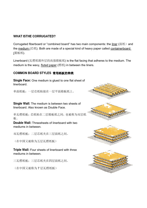
WHAT ISTHE CORRUGATED?Corrugated fiberboard or "combined board" has two main components: the liner (面纸)and the medium (芯纸). Both are made of a special kind of heavy paper called containerboard (箱板纸).Linerboard (瓦楞纸箱外层的高强箱板纸) is the flat facing that adheres to the medium. The medium is the wavy, fluted paper (楞纸) in between the liners.COMMON BOARD STYLES 常用纸板的种类Single Face: One medium is glued to one flat sheet oflinerboard.单面纸板:一层芯纸粘接在一层平面箱板纸上。
Single Wall: The medium is between two sheets oflinerboard. Also known as Double Face.单瓦楞纸板:芯纸粘在二层箱板纸之间,也被称为双层纸板。
Double Wall: Threesheets of linerboard with twomediums in between.双瓦楞纸板:二层芯纸夹在三层面纸之间。
(在中国又被称为五层瓦楞纸板)Triple Wall: Four sheets of linerboard with threemediums in between.三瓦楞纸板:三层芯纸夹在四层面纸之间。
(在中国又被称为7层瓦楞纸板)Flutes 楞形Architects have known for thousands of years that an arch(拱) with the proper curve (曲线) is the strongest way tospan a given space (跨越一个给定的空间). The inventorsof corrugated fiberboard applied this same principle to paperwhen they put arches in the corrugated medium(瓦楞芯纸).These arches are known as flutes (楞)and when anchoredto the linerboard with adhesive, they resist bending andpressure from all directions.When a piece of combined board is placed on its end, the arches form rigid columns, capable of supporting a great deal of weight. When pressure is applied to the side of the board, the space in between the flutes acts as a cushion(垫子)to protect the container's contents. The flutes also serve as an insulator (绝缘体, 绝热器,保温层), providing some product protection from sudden temperature changes. At the same time, the vertical linerboard provides even more strength and protects the flutes from damage.Flutes come in several standard shapes or flute profiles (A, B, C, E, F, etc.). A-flute (A楞)was the first to be developed. B-flute was the next and is much smaller than A-flute. C-flute followed and is between A and B in size. It is also the most common large flute profile.E-flute is smaller than B and F-flute is smaller yet. Due to variances in flute sizes between manufacturers, FBA no longer publishes flute guidelines.In addition to these five most common profiles, new flute profiles—both larger and smaller than those listed here—are being created for more specialized boards. Generally, larger flute profiles deliver greater vertical compression strength (垂直压力)and cushioning, while smaller profiles provide better resistance to process and printing crush.Different flute profiles can be combined in one piece of combined board. For instance, in a triple wall board, one layer of medium might be A-flute while the other two layers might beC-flute. Mixing flute profiles in this way allows designers to manipulate the compression strength, cushioning strength (减震强度、缓冲强度) and total thickness of the combined board.Corrugated BasicsWhat is Corrugated?Corrugated boxes are easy to recognize. Corrugated is made ofpaper and has an arched layer, called "fluting," between smoothsheets, called "liner." The corrugated most commonly used tomake boxes has one layer of fluting between two smoothsheets. But there are many types of corrugated available, eachwith different flute sizes and thicknesses(厚度).Corrugated is an extremely durable, versatile, economical and lightweight material used for custom-manufactured shipping containers(运输容器), packaging and point-of-purchase displays(销售展示包装,即所谓POP展示包装), in addition to numerous non-traditional applications ranging from pallets(货盘、托盘)to children's toys to furniture.Why Corrugated?Corrugated. It's not just a brown box.Corrugated is a complete, high-performance material design, manufacturing and delivery system. Corrugated is the preferred packaging material because it is:1. Durable2. Versatile3. Lightweight4. Environmentally Friendly5. High-Tech6. Customizable7. Protective8. Graphically Appealing9. Cost-EffectiveIf it's not just a cardboard box, what is it?A High-Tech Engineered Material.What may come as a big surprise to many is that the ever-present corrugated "cardboard box" is high-tech:1. Ongoing R&D (研发)programs continuously improve such characteristics asstrength-to-weight ratios(强度与重度的比率), printability, moisture barriers (潮气阻隔) and recyclability.2. Corrugated components, designs and end products are manufactured on sophisticated,automatic equipment that reduces costs and ensures consistent performance.3. The vast majority of corrugated products are designed and prototyped with advanced,computer-aided design (CAD)and manufacturing systems, providing customers with the best and most cost-effective solutions to their packaging challenges.Infinitely Customizable.Corrugated offers thousands of possible combinations of board types, flute sizes (caliper), basis weight, adhesives, treatment and coatings, including flame retardant and static control protection.Corrugated is the only rigid shipping container and packaging medium that can be cut and folded into an infinite variety of shapes and sizes and direct-printed with high-resolution color graphics (including lithography, flexography and silk screening). And corrugated is not just for displays and boxes. Other uses include low-cost, one-way recyclable pallets, retail bulk bins, and lightweight castles that children can build themselves.There are hundreds of basic designs and thousands of adaptations, each chosen on the basis of proven experience and the proposed use of the product.Corrugated is routinely custom-designed to fit specific product protection, shelf space and shipping density requirements (including inner packaging that prevents shifting).Tenaciously Protective.Corrugated combines structural rigidity with superior cushioning qualities. Containers, packages and pallets nest products in an optimally protective environment, so even heavy or fragile contents arrive undamaged.Corrugated offers excellent tear, tensile and burst strength to withstand shipping pressures.It resists impact, drop and vibration damage while offering uniform stacking and weight distribution so the load stays put, regardless of the form of transportation.Corrugated can be designed to contain flowable, granular or loose bulk products and even hazardous materials. It is also used to ship liquids and fresh foods, with the addition of removable plastic or waxed liners which serve as moisture barriers.All this from a material that is lightweight, low-cost and recyclable.Graphically Appealing.Corrugated containers and packaging are mobile billboards that create product image wherever they travel. Corrugated displays are eye-catching modular units that can be set up quickly and recycled at the end of a promotion.Corrugated is a very flexible medium that accommodates a wide range of printing options to support the end-use requirement:1. Offset lithography and rotogravure (high-volume).2. Flexography or letterpress (shorter runs)3. Silk screening (displays)4. Corrugated can be direct printed in plant or manufactured with high-end process colorgraphics.Preeminently Cost-Effective.One of the least expensive containers ever developed, the overall cost of corrugatedshipping containers is usually between one percent and four percent of the value of the goods they carry.The cost of labor and tools required to produce, fill, and move the container is low. The cost of shipping is low, due to lower weights and higher fill densities than alternative packaging.The trend toward light weighting will continue to drive down shipping costs. Low raw material costs and mass production of corrugated containers makes them particularly cost-efficient.The ultimate contribution to cost reduction is when corrugated is used as an all-in-one shipping, storage, advertising and display medium - a growing trend both in warehouse and other retail stores.Environmentally Responsible.Corrugated, made from a natural renewable resource, has a great environmental record. Corrugated is frequently manufactured using high percentages of secondary fiber (including old corrugated containers, kraft, old newspapers and even straw), thereby diverting these materials from the municipal solid waste stream.In 2004, more than 24 million tons of corrugated were recovered and recycled in the U.S. -- that's 73 percent of all containerboard produced in the same year. Corrugated has the best recycling rate of any packaging material used today.In addition, the use of corrugated constructions with high-performance linerboard has led to a significant overall reduction in basis weight and a significant source reduction of raw materials.Water-based inks are now used almost exclusively for printing graphics on corrugated containers, avoiding the use of lead-based inks and solvents which pollute the air and the water used to wash down printing equipment between color changes.Box DimensionsDimensions are given in the sequence of length, width and depth. Internationally, the words length, breadth and height may be used to express these dimensions. The dimensions of a box are described based on the opening of an assembled box, which can be located on the top or the side, depending on how it is to be filled. The opening of a box is a rectangle; that is, it has two sets of parallel sides. The longer of the two sides is considered its length, the shorter of the two sides is considered its width. The side perpendicular to length and width is considered the depth of the box.Dimensions can be specified for either the inside or the outside of the box. Accurate inside dimensions must be determined to ensure the proper fit for the product being shipped or stored. At the same time, palletizing and distributing the boxes depends on the outside dimensions. The box manufacturer should be informed as to which dimension is most important to the customer.。
- 1、下载文档前请自行甄别文档内容的完整性,平台不提供额外的编辑、内容补充、找答案等附加服务。
- 2、"仅部分预览"的文档,不可在线预览部分如存在完整性等问题,可反馈申请退款(可完整预览的文档不适用该条件!)。
- 3、如文档侵犯您的权益,请联系客服反馈,我们会尽快为您处理(人工客服工作时间:9:00-18:30)。
High-rate flame synthesis of vertically aligned carbonnanotubes using electric field controlWilson Merchan-Merchan a ,Alexei V.Saveliev b ,Lawrence A.Kennedyb,*aDepartment of Materials Sciences and Engineering,University of Illinois at Chicago,Chicago,IL 60607,USAbDepartment of Mechanical and Industrial Engineering,University of Illinois at Chicago,851South Morgan Street,Chicago,IL 60607,USAReceived 31July 2003;accepted 17December 2003AbstractThe electric field controlled synthesis of carbon nanomaterials on a Ni-based catalytic support positioned at the fuel side of the opposed flow oxy-flame is studied experimentally.Carbon nanomaterials formed on the probe surface are comparatively analyzed for two characteristic operational modes:a grounded probe mode and a floating probe mode.In a grounded mode a number of various carbon nanostructures are formed depending on the probe location in flame.Observed nanoforms include multi-walled carbon nanotubes (MWNTs),MWNT bundles,helically coiled tubular nanofibers,and ribbon-like coiled nanofibers with rectan-gular cross-section.The presence of various carbon nanoforms is attributed to the space variation of flame parameters,namely flame temperature and concentration of chemical species.It is found that the presence of an electric potential (floating mode operation)provides the ability to control the nanostructure morphology and synthesis rate.A thick layer (35–40l m)of vertically aligned carbon nanotubes (VACNTs)is found to be formed on the probe surface in the floating potential mode.This layer is characterized by high uniformity and narrow distribution of nanotube diameters.Overall,the electric field control method demonstrates sta-bilization of the structure in a wide flame region while growth rate remains dependent on flame location.Ó2004Elsevier Ltd.All rights reserved.Keywords:A.Carbon nanotubes;B.Catalyst support;C.Scanning electron microscopy1.IntroductionIn recent years great effort has been devoted to the study of synthesis of carbon nanotubes in flames.Since the discovery of nanotubes in 1991by Iijima [1]con-ventional methods such as arc plasma discharges [2,3],pulsed laser vaporization [4],and chemical vapor deposition (CVD)[5]have dominated the field.Re-cently,it has been demonstrated in a number of publi-cations that flames can be applied as a relatively inexpensive,robust,pyrolysing carbon source for growing tubular nanomaterials [6–14].Mainly studies in co-flow diffusion flames with the introduction of a cat-alyst in the form of nano-aerosol or in the form of solid support have been reported.Yuan et al.[6]analyzed flame-based growth of nanotubes on a Ni/Cr support in laminar co-flow methane–air diffusion flames.Forma-tion of entangled MWNTs with a diameter range of 20–60nm was reported.In related work,Yuan and co-workers [7]used a catalytic support in the form of a stainless steel grid to produce MWNTs in an ethylene–air diffusion flame.The electroplating of the grid with cobalt resulted in synthesis of aligned MWNTs.The metal catalyst dispersed on TiO 2substrate was used by Vander Wal [8]to generate MWNTs in ethylene/air and acetylene/air diffusion co-flow flames.It was demon-strated that the structure of the obtained nanotubes and nanofibers strongly depends on the catalytic particle shape and chemical composition.Recently,Vander Wal and co-workers [9,10]also reported that single-walled carbon nanotubes (SWNTs)can be grown in premixed co-flow flames by seeding the fuel line with ferrocene and compositions of metal nitrates serving as catalyst precursors for the formation of nanotubes.It was demonstrated that ferrocene and Fe nanoparticles can yield bundles of self-assembled single-wall nanotubes with diameters as small as two nanometers.The rich premixed flame synthesis of carbon nanotubes using supported catalyst [11]was optimized by selection of optimal flame conditions including fuel composition and*Corresponding author.Tel.:+1-312-996-2400;fax:+1-312-996-8664.E-mail address:lkennedy@ (L.A.Kennedy).0008-6223/$-see front matter Ó2004Elsevier Ltd.All rights reserved.doi:10.1016/j.carbon.2003.12.086Carbon 42(2004)599–608fuel-to-air ratio.The studied fuels include methane, ethane,ethylene,acetylene,and propane.A recent work by Height and co-workers[12]used premixed co-flow flames to grow SWNTs.A detailed characterization of SWNT growth was given with emphasis onflame posi-tion andflame air-to-fuel ratio.The non-catalytic for-mation of carbon nanotubes was reported in opposed flow oxygen enrichedflame studies[13].The strong potential of theseflames for carbon nanomaterial syn-thesis was recently proven employing a catalytic probe [14].If compared with CVD and plasma methods,a typi-calflame is a reacting medium characterized by strong thermal and chemical non-uniformity.It is not surpris-ing,that a number offlame studies show a high mor-phological and growth rate sensitivity of formed carbon nanomaterials to theflame location.An efficient control method is required to improve uniformity and produc-tivity offlame based synthesis and utilization of elec-tromagneticfield control is one of the promising approaches.The electricfield control is successfully tested in chemical vapor deposition(CVD)and plasma synthesis studies[15–21]as reported recently by several authors:Kuzuya et al.[15]applied an electricfield for effective control of producing helically coiled carbon materials using CVD;Avigal et al.[16]grew short aligned nanotubes by positively biasing the substrate during the nanotube formation in CVD;Srivastava et al.[17]showed that nanotubes that are grown under the influence of an electricfield in plasma can permanently maintain their alignment when the electricfield force is removed;Lee et al.[18]using CVD and magneticfields showed that it is possible to grow aligned carbon na-notubes at any angle with respect to the substrate sur-face;Ural et al.[19]used CVD to grow carbon nanotubes with and without the influence of electric fields to show the ability of electricfields to grow aligned carbon nanotubes;Colbert et al.[20]used an arc plasma discharge to show that an electricfield is essential for nanotube growth by stabilizing the open tip and pre-venting it from closure;Srivastava et al.[21]used plas-ma varying voltages to study the size,length,and alignment of carbon nanotubes.To our knowledge,electricfields have not been ap-plied to control growth of carbon nanotubes inflames prior to this study.In this article the carbon nanoforms formed on a catalytic probe in opposedflow oxy-flame are comparatively analyzed for various probe potentials. It is shown that implementation of an electricfield control allows to increase their structural uniformity and growth rate.2.ExperimentalFig.1shows the schematic of the experimental setup employed in the present study.A counter-flow burner forms two opposite streams of gases;the fuel(methane seeded with4%of acetylene)is supplied from the top nozzle and the oxidizer(50%O2+50%N2)is introduced from the bottom nozzle.The fuel and oxidizerflows impinge against each other to form a stable stagnation plane,with a diffusionflame established from the oxi-dizer side.The introduction of co-flowing nitrogen through a cylindrical annular duct around the outer edge of the oxidizer nozzle has the function of extin-guishing theflame near the outer jacket and isolating it from the environment.A detailed description of the burner is given by Beltrame et al.[22].Technical purity methane(98%,AGA Gas Inc.)was seeded with atomic absorption purity acetylene(99.8%,AGA Gas Inc.).The experiments were conducted with constant fuel and oxidizer velocities and a strain rate equal to20sÀ1.A40mm long catalytic probe was introduced through theflame-protecting shield to the yellow soot-containing region of theflame.The central part oftheFig.1.Schematic of the experimental setup.600W.Merchan-Merchan et al./Carbon42(2004)599–608probe($25mm)was used to study the structure of deposited materials.The0.64mm diameter probe is an alloy with compositions of73%Ni+17%Cu+10%Fe. The axial position of the probeðZÞwas controlled by the positioning system.Reported experiments were con-ducted with residence time of10min.To generate radial electricfields on the probe surface, the probe was supported on Teflonâisolators while the burner nozzles were kept at ground potential(Fig.1).In general this configuration allows to generate a variety of electricfields controlling the probe potential with the external electric source.In the present work,experi-ments were conducted at two characteristic probe potentials:grounded probe and probe atfloating po-tential.When nodes one and two are connected no electric field is generated;this mode is further referred as the grounding probe mode(GPM).On the other hand, when node one and two are disconnected,electricfield is generated between the surface of the catalytic probe and the edges of the fuel and oxidizer nozzles;this configu-ration is further referred as thefloating potential mode (FPM).Due to the small size of the probe relative to size of the burner nozzles the electricfield around the probe can be well approximated as radial.The source of the floating potential is the transport of ions and electrons formed in high-temperature oxygenflame to the probe surface;a potential difference close to300mV was typically measured when the probe was in FPM.The initial surface scans of the catalyst probe were performed by a scanning electron microscope(JEOL Inc.,Model JSM-6320F)with a coldfield emission source.The specimens for TEM examinations were prepared by ultrasonic dispersion of carbon deposits collected from a specific probe location in acetone;a drop of the suspension was placed on the electron microscope grid.The detailed structural characteristics of the deposited material were obtained from high-res-olution electron microscopy studies performed in a JEOL JEM-3010electron microscope with the magnifi-cation range from50to1,500,000times.Images were collected on a Gatan digital imaging system and pro-cessed by Digital Micrograph software.3.Results and discussionWhen the catalytic probe was inserted in GPM a variety of carbon nanostructures were observed depending on position of catalytic probe in the fuel zone of the opposedflowflame.Those carbon structures in-clude MWNTs and MWNT bundles,nanofibers with varying degree of crystallinity,helical regularly coiled tubular carbon nanotubes,ribbon-like coiled nanofibers with rectangular cross section,and,finally,long($0.2 mm)uniform-diameter($100nm)tubular nanofibers with regular internal structure of carbon layers.Some of the observed structures,such as coiled tubular and rib-bon-like nanofibers,have been reported[23,24]to grow only under special conditions in CVD.Fig.2(a)shows a typical regularly coiled carbon nanofiber formed in ourflames.The diameters of these coils ranged from20to100nm with lengths of several microns.These structures were typically observed in the zone close to Z¼9mm,in the vicinity of theflame front.Qualitatively,the formation of helical nanotubes can be explained by variation of deposition rates and, hence,extrusion velocities along the contact curve be-tween the active catalytic particle and thealready Fig.2.SEM images of carbon nanomaterials grown in various loca-tion of the opposedflowflame on a single catalytic support:(a)heli-cally coiled spiral carbon nanotube,(b)multi-walled carbon nanotubes,(c)coiled carbon nanofiber with rectangular cross-section.W.Merchan-Merchan et al./Carbon42(2004)599–608601formed tube[23].The sharp gradients of temperature and chemical species in the vicinity of theflame zone induce sensible variations of carbon deposition rates providing the condition for the growth of helical struc-tures.Irregular carbon nanotubes are widely observed in theflame region close to Z¼8:5mm.They form a coating layer that typically contains entangled web of randomly directed tubes,carbon nanofibers and soot particulates,as shown in Fig.2(b).The tube diameters vary significantly,typically from10to45nm.The internal tube structure is regular,although carbon layers often form an angle with the tube axis.As a result bamboo-like structures are widely observed.Irregularly oriented nanotubes frequently change direction of growth;kinks and bends are common for these struc-tures.The other distinctive coiled carbon structure observed in ourflames possesses a nontubular form,Fig.2(c). These structures are typically found to be present in the low temperature zone Z¼8mm.The nanofiber has a distinctive ribbon-like appearance with unwound ribbon rolls.The rectangular cross section has a height of300 nm and a thickness of100nm.It was reported previously [25],that growth of these rarely observed ribbon-like filaments could be catalyzed by small iron-containing particles in CO containing atmosphere at700°C,which correspond to theflame environment at the vicinity of Z¼8mm.The variation of structure and morphology of formed carbon nanomaterials is directly attributed to the strong variation of temperature and chemical composition in the studiedflame region.The distributions of several major hydrocarbons(CH4,C2H2,CO,and C6H6)that can contribute to the growth of carbon deposits are shown in Fig.3along with the temperature profile[22]. It is easy to conclude that all above components vary significantly in theflame region of interest.Thus,con-centration of CH4and C2H2diminishes below100ppm for Z>10:5mm;the concentration of CO grows with Z reaching its maximum at this point;C6H6is present in essential quantities only from8to10mm,maximizing at 9.5mm.The essential variations of temperature and chemical composition are inevitable in a variety offlame config-urations.The effective control method is necessary to stabilize growth of carbon nanomaterials with specified structure and morphology.The electricfield control method was implemented in this study electrically insulating the probe from the grounded support and operating it at afloating potential.The catalytic probe of the same metallic composition was inserted at the axialflame position of Z¼8:5mm in FPM(approximate probe potential)300mV).The produced carbon deposits were analyzed with SEM (Figs.4and5).Fig.4shows that controlled electricfield growth generates a coat of VACNTs.Low magnifica-tion image shows that VACNT layer uniformly coat the catalytic substrate.The generated nanotubes are char-Fig.4.SEM image of orderly VACNT layer covering the probe sur-face;floating potential mode,Z¼8:5mm.The layer is partially re-moved revealing the bare catalytic surface.Fig.5.High-resolution SEM of the wall edge of the layer shown in Fig.4displays nanotube purity and alignment.602W.Merchan-Merchan et al./Carbon42(2004)599–608acterized by high purity and alignment,as shown in Fig.5.For this axial position,hundreds of nanotube diam-eters were measured.The results show a very narrow diameter distribution with a mean diameter close to 38nm.Fig.2(b)and Figs.4,5depict the carbon nanomate-rials grown on identical probes in the same flame loca-tion respectively in GPM and FPM conditions.Analysis of SEM images on the synthesized carbon materials on both catalytic substrates suggests that nanotube growth is greatly enhanced when the electric field is present (FPM)if compared with the case when the electric field is absent (GPM).Other interesting aspects,displayed in Figs.4and 5,include not only the presence of VACNTs but also the absence of contaminants such as soot or other nontubular carbon structures that are often pres-ent in the flame synthesis of carbon nanotubes.It should be noted that the samples analyzed in this study were never purified by any kind of chemical and/or physical treatment.With electric field stabilization,flame position re-mains the important factor in controlling the thickness of the coat layer of nanotubes formed under FPM.Figs.6and 7show the variation of nanotube formation along the burner axis.Fig.6is a low resolution SEM image of the catalytic substrate inserted in the FPM at the axial distance of Z ¼9:5mm.The well-defined layer formed here shows highly ordered carbon nanotube arrays,similar to those found in the previous position.The application of high-resolution imaging in Fig.6reveals a highly dense bundle of nanotubes attached to the tips of the undisturbed nanotube layer,as shown in Fig.7.High-resolution imaging shows that these nanotube bundles are free of contaminants as well.It is evident by comparing micrographs obtained at the axial position of Z ¼8:5mm to those obtained at Z ¼9:5mm that the thickness of the coating layer decreased when the sub-strate is inserted further down from the edge of the fuel nozzle.Several SEM images were collected at variouslocations of the probe surface;an average layer thick-ness of 9l m was measured for this flame location.Another interesting aspect of these nanotube layers is the strong van der Waals body attraction force existing between the tubes in the self-formed macro bundles.This aspect is unique since it greatly simplifies their harvesting.That is,micron size arrays of VACNTs can be easily removed from its roots.A catalytic substrate inserted at the axial flame po-sition of Z ¼10:5mm shows no apparent sign of arrays of VACNTs (Fig.8).But high-resolution SEM reveals that thinner and less uniform layers of VACNTs are still being grown as shown in Fig.9.The nanotube layer at this position is still aligned and defined but not as well as in the two previous positions.It can be speculated that at this flame position the conditions of CNT growth are far from optimal and the electric field control has only limited effect.A thickness of VACNT arrays of 3l m is characteristic for this flame position.Additionally,high and low resolution SEM analysis was performed on the surface of the support catalytic substrate at different locations in order to confirm the uniformity of the nanotube layer.In this particular experiment,the probe was inserted into the flame ataFig.6.Low resolution SEM image shows the catalyst substrate coated with a layer of carbon nanotubes (FPM),Z ¼9:5mm.Fig.7.Higher resolution SEM of a micro area in Fig.6.Fig.8.Low resolution SEM image on the catalyst substrate coated with a layer of carbon material (FPM),Z ¼10:5mm.W.Merchan-Merchan et al./Carbon 42(2004)599–608603position where the most thick layer of nanotubes were observed,Z¼8:5mm.After the exposure to theflame, the probe was placed on a stainless steel stud for microscope studies.Fig.10represents SEM images of arrays of orderly and high purity nanotubes scanned at top,center,and bottom of the probe surface,respectively.For all probe locations considered for microscopic analysis,arrays of nanotubes covered the probe with orientation perpen-dicular to the probe surface.By inspection of Fig.10it is evident that most of the formed material remains at-tached to the surface.Higher resolution SEM on the walls of this material showed that the bulk material is composed of arrays of nanotubes.The separated mate-rial always tends to remains packed like bundles of hay and always maintains its original length.In the upper right corner of Fig.10(b)a bundle of highly dense na-notubes is observed.This bundle has a cylindrical shape and a length of approximately40l m which coincide with the length of nanotubes in the attached VACNT layer.The material remains packed due to the strong van der Waals forces that exist between the tubes in the bundles.The same sample probe was then rotated180°for further SEM scanning and again,layers of nanotu-bes were present covering the catalytic substrate surface.High-resolution TEM was employed to study the inner morphology of the aligned nanotubes.For TEM studies,nanotubes formed on the catalytic support were carefully peeled offand transferred to acetone.After sonication,the drop of the suspension was placed ona Fig.9.Higher resolution SEM of a micro area in Fig.8.Fig.10.Low and high resolution(inserts)SEM images of scanned probe surface showing uniformity of VACNT coating layer.604W.Merchan-Merchan et al./Carbon42(2004)599–608copper-substrate/carbon-film of microscope specimen grid and dried.TEM images of nanotubes synthesized at Z ¼8:5mm are shown in Figs.11and 12.Very low resolution TEM imaging on the transferred material shows the presence of high-density closely packed nanotube bundles (Fig.11).It appears that even after sonication,closely packed bundles of nanotubes remain intact.Fig.11shows typical bundles of nanotubes ob-served by TEM in a sample grid,here the bundle pos-sesses a length and width of 31and 10l m,respectively.In a closer zoom on the nanotube bundle,no material other than tubular structures are present,Fig.12.From a number of micrographs the average diameter of the cylindrical multi-shells was measured,a monodisperse diameter distribution averaging 38nm was obtained.The application of high-resolution TEM imaging on these carbon nanotubes reveals a texture of well-aligned and highly graphitized concentric graphitic cylinders.The average interplanar distance of the concentric cylindrical graphene sheets was measured to be 0.34nm,as indicated in Fig.13.The layer planes appear to be perfectly parallel to the central tube axis.The experimental results show the strong influence of the electric field on alignment,size distribution,internal structure,and growth rate of carbon nanotubes.The mechanism of alignment is widely discussed in the lit-erature [26–28].As an example,employing a plasma discharge Merkulov and coworkers [27]successfully demonstrated,that the direction of the electric field lines determines the orientation of the carbon nanotubes and nanofibers;electric field alignment of single-walled na-notubes were considered by Zhang et al.[28].Consider the alignment mechanism of a single CNT growing on a metal catalytic support at the presence of the electric field E (Fig.14a).At the synthesis tempera-ture,both metallic and semiconducting CNT can be treated as good conductors.Consequently,the nanotube can be represented as a conductive cylinder of length L and radius R in contact with a conducting plane with a surface charge density r .For a cylinder of finite length,an electric field generated by the plate in the normal direction will induce a bound charge at the nanotube end to screen the external field over the nanotube vol-ume.The field-screening area of the single nanotube can be estimated as L 2.Accordingly,the total charge of the nanotube is q %r L 2¼e 0L 2E .The total electrostatic force acting on the nanotube is F %qE ¼e 0L 2E 2.The nanotube inclined at an angle h with respect to the normal direction will have axial F a and tangential F t components of the force F inducing respectively axial stress and alignment force.For a small deviation of the nanotube from the normal direction d ,the alignment force F t ¼F sin h ¼e 0LE 2d is proportional to the nano-tube length.The more rigorous solution of the electro-static problem [29]gives an expression for the total electrostatic force acting on the cylinder as F ¼pe 0E 2L 2=ðln ð2R =L ÞÀ3=2Þ,showing that the acting force is a weak function of R .The solution also shows the pres-ence of finite surface charges over the lower part of the nanotube with the charge density distribution close tolinear.Fig.11.Low resolution TEM image of material removed from the catalytic support.The material is produced using FPM at Z ¼8:5mm.Fig.12.TEM image of metal catalyzed carbon nanotubes from a micro area shown in Fig.11.Fig.13.High-resolution TEM image of the wall of a tubule produced in floating potential mode.W.Merchan-Merchan et al./Carbon 42(2004)599–608605For CNTs growing on a conductive substrate as a vertically aligned array with a tube-to-tube separation distance of D,the externalfield is reduced by mutual screening(Fig.14b).The depth of thefield penetration can be also estimated as D.Similar consideration for the charge induced on the nanotube tip provides estimation of the charge value q%e0D2E and the electrostatic force acting on the single tube F%qE¼e0D2E2.Conse-quently,the aligning force F t¼e0DE2d is linearly pro-portional to the nanotube separation D and the deviation from the vertical position d.The surface charges of the same polarity induced near the nanotube ends ensure their separation and alignment.These repulsive forces overcome van der Waals attraction forces.It is worth mentioning that the repulsive align-ment is quiet different from the alignment induced by van der Waals interactions.The latter mechanism leads to the formation of nanotube bundles which in turn reduces the thermal randomization of the CNT growth. However,a direction of the bundle growth remains arbitrary.Overall,the electricfields near the tips of growing nanotubes can be extremely high.Even applied poten-tials as small as few tens of millivolts can develop an electricfield exceeding1000V/cm at the characteristic nanotube diameter.The experimentally measuredfield enhancement factors are reaching800for multi-walled nanotubes[30]and3000for single-walled nanotubes [31].The enhancement of the electricfield at the tip of closed conducting nanotube was calculated by Maiti et al.[32];the resulting force estimated from the axial stress is in a good agreement with Taylor solution[29].The important aspect of the aligned growth is that the constant orientation of catalytic particles at the tips of the growing nanotubes is preserved by the electricfield. The non-symmetric catalytic particle is polarized in the electricfield,and the induced dipole moment tends to be aligned along the electricfield lines.The formation of helical and spiral nanotubes requires variation of the particle orientation.As a result the constant orientation of the catalytic particle stabilizes the linear CNT struc-tures.The high concentration of the electric charges near the nanotube end also induces axial stress between the growing nanotube body and conductive catalyst parti-cle.This can lead to the increase of the CNT growth rate.For clarity,we further consider a nanotube with a catalytic particle at the tip.The tip-growth proceeds via several important stages,including decomposition of flame hydrocarbons on catalytic surface,diffusion of carbon through and over metal particulate,formation of ordered CNT structure on the opposite side of the catalytic particle.The solution of electrostatic problem suggests strong concentration of charge and electricfield near the tip of the growing nanotube,namely on the catalytic particle attached to the nanotube end.The stress introduced between the particle and the CNT body may be estimated as r s¼F=p R2.While the force F has only weak dependence on R,the stress shows dra-matic increase with the reduction of contact area and can reach a critical value rÃscorresponding to the pos-sible particle separation.This can discriminate the growth of nanotubes with R<RÃ.The moderate value of stress,however,can increase the transformation of carbon to the CNT structure.As a result the concen-tration of free carbon on the CNT side will decrease leading to the faster carbon diffusion and the CNT growth will proceed at the increased rate.The sensitiv-ity of the stress to the nanotube diameter is a possi-ble explanation for the narrow diameter distribution which is characteristic for the synthesized VACNT arrays.Finally,the electricfield can influence the transport of charged particles inflames that include ions and charged soot particles.In this way,soot entrapment in the growing layer can be controlled by the electricfield.The effect of the electricfield control using various electricfield amplitudes and geometries is an interesting subject for the future studies.The selectedflame con-figuration allows ease of application of internal(probe generated)and external(generated by external elec-trodes)electricfields,as well as time-dependent elec-tromagneticfields.4.ConclusionsThe electricfield controlled synthesis of carbon nanomaterials on a Ni-based catalytic support posi-tioned at the fuel side of the opposedflow oxy-flame is studied experimentally.Theflame environment is formed by fuel and oxidizer with compositions of CH4+4%C2H2and50%O2+50%N2,respectively.Car-bon nanomaterials formed on the probe surface are comparatively analyzed for two characteristic opera-tional modes:a grounded probe mode and afloating probe mode.In a grounded mode a number of various carbon nanostructures are formed depending on the probe location inflame.Observed nanoforms include multi-walled carbon nanotubes(MWNTs),MWNT bundles, helically coiled tubular nanofibers,and ribbon-like coiled nanofibers with rectangular cross-section.The presence of various carbon nanoforms is attributed to the space variation offlame parameters,namelyflame temperature and concentration of chemical species.It is found that a presence of an electric potential (floating mode operation)provides an ability to control nanostructure morphology and synthesis rate.A thick layer(35–40l m)of vertically aligned carbon nanotubes (VACNTs)is found to be formed on the probe surface in thefloating potential mode.This layer is character-ized by high uniformity and narrow distribution of nanotube diameters.Electricfield control method demonstrates stabilization of the linear nanotube structure in a wideflame region.The growth rate re-mains dependent onflame location but the strong enhancement effect is observed with application of electricfield.AcknowledgementsThis work was supported by the National Science Foundation grant CTS-0304528.This work was par-tially supported by the Air Liquide Corp.under an Unrestricted Laboratory Development Grant.The au-thors extend special thank to Dr.Alan Nicholls,Mr. John Roth,Ms.Linda J.Juarez,and Ms.Kristina Jarosius from the UIC Research Resource Center for day-to-day assistance in SEM and TEM studies, encouragement and helpful discussions.The authors would also like to thank Mr.Attilio Milanese for his input and helpful discussions.References[1]Iijima S.Helical microtubules of graphitic carbon.Nature1991;354:56–8.[2]Kiang CH,Goddard WA,Beyers R,Salem JR,Bethune DS.Catalytic synthesis of single-layer carbon nanotubes with wide range of diameters.J Phys Chem1994;98:6612–8.[3]Shi Z,Lian Y,Zhou X,Gu Z,Zhang V,Iijima S,et al.Massproduction of single-wall carbon nanotubes by arc discharge method.Carbon1999;37:1449–53.[4]Guo T,Nikolaev P,Thess A,Colbert DT,Smalley RE.Catalyticgrowth of single-walled nanotubes by laser vaporization.Chem Phys Lett1995;243:49–54.[5]Andrews R,Jacques D,Rao AM,Derbyshire F,Qian D,Fan X,et al.Continuous production of aligned carbon nanotubes:a step closer to commercial realization.Chem Phys Lett1999;303:467–74.[6]Yuan L,Saito K,Pan C,Williams FA,Gordon AS.Nanotubesfrom methaneflames.Chem Phys Lett2001;340:237–41.[7]Yuan L,Saito K,Hu W,Chen Z.Ethyleneflame synthesis of well-aligned multi-walled carbon nanotubes.Chem Phys Lett2001;346: 23–5.[8]Vander Wal RL.Flame synthesis of substrate-supported metal-catalyzed carbon nanotubes.Chem Phys Lett2000;324:217–23.[9]Vander Wal RL,Lee JH.Ferrocene as a precursor reagent formetal-catalyzed carbon nanotubes:competing effbust Flame2002;130:27–36.[10]Vander Wal RL.Fe-catalyzed single-walled carbon nanotubesynthesis within aflame bust Flame2002;130: 37–47.[11]Vander Wal RL,Hall LJ,Berger GM.Optimization offlamesynthesis for carbon nanotubes using supported catalyst.J Phys Chem2002;B106:13122–32.[12]Height MJ,Howard JB,Tester JW.Synthesis of single-walledcarbon nanotubes in a premixed acetylene/oxygen/argonflame.Proceedings of the Third Joint Meeting of the U.S.Section of the Combustion Institute(2003).[13]Merchan-Merchan W,Saveliev A,Kennedy LA,Fridman A.Formation of carbon nanotubes in counter-flow,oxy-methane diffusionflames without catalyst.Chem Phys Lett2002;354:20–4.[14]Saveliev A,Merchan-Merchan W,Kennedy LA.Metal catalyzedsynthesis of carbon nanotubes in an opposedflow methane oxygenflbust Flame2003;135:27–33.[15]Kuzuya C,Kohda M,Hishikawa Y,Motojima S.Preparation ofcarbon micro-coils with the application of outer and inner electromagneticfields and bias voltage.Carbon2002;40:1991–2001.[16]Avigal Y,Kalish R.Growth of aligned carbon nanotubes bybiasing during growth.Appl Phys Lett2001;78(16):2291–3. [17]Srivastava AK,Srivastava ON.Curious aligned of carbon nano-tubes under applied electricfield.Carbon2001;39:201–6. [18]Lee KH,Cho JM,Sigmund W.Control of growth orientation forcarbon nanotubes.Appl Phys Lett2003;82(3):448–50.[19]Ant U,Yiming L,Hongjie D.Electric-field-aligned growth ofsingle-walled carbon nanotubes on surfaces.Appl Phys Lett 2002;81(18):3464–6.[20]Colbert DT,Smalley RE.Electric effects in nanotube growth.Carbon1995;33(7):921–4.[21]Srivastava A,Srivastava AK,Srivastava ON.Effect of externalelectricfield on the growth of nanotubules.Appl Phys Lett1998;72(14):1685–7.W.Merchan-Merchan et al./Carbon42(2004)599–608607。