FJA4210OTU;FJA4210RTU;中文规格书,Datasheet资料
JetWave 4020 4020E系列工业级802.11ac + 802.11n 2.4G WIF
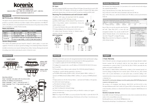
AppearanceJetWave 4020/4020E SeriesIndustrial 802.11ac + 802.11n 2.4G WIFI AP, 2xGT + USB M12Quick Installation Guide V1.0R&TTE Directive 1999/5/EC DeclarationThe product may be operated in all European Union countries. While you see the CE Marking printed on our product, it indicates the product complies with the requirement of the R&TTE (1995/5/EC) Directive. You can download the formal document of the product from our Web site or send inquiry to our Sales/Technical people.Only trained and qualified personnel should be allowed to install, replace, or service this equipment. The device can only be operated according to the technical specification. Read the installation instructions/user manual, including Power, Cable, Antenna, Warning info and well Grounding is must before connecting the system to the power source.DC InputThe device supports dual DC power input or Passive PoE input, the typical power source is DC 24V (±15%) or DC 110V depends on the model you purchase. For passive PoE input, please purchase the injector from us, the device do NOT accept force mode from PSE switch.The Korenix View Utility provides you convenient tool to scan the network and configure the connected Korenix device.Step 1: Open the Korenix View Utility. (Must later than V1.6.11)Step 2: Select the correct NIC (Network Interface Card) from the NIC list.Step 3: Click “Discovery”, and then the Nodes and its IP address can be found and listed in Node list.Step 4: After you scan the network, select the deviceand click “Open Web GUI” to access the web management interface. You can also modify the IP address/Netmask directly on the selected entry and then click “Change IP“ to change IP settings.Note: Please check the User Manual to configure theother software settings.3 Years WarrantyEach of Korenix’s product is designed, produced, and tested with high industrial standard. Korenix warrants that the product(s) shall be free from defects in materials and workmanship for a period of three (3) years from the date of delivery provided that the product was properly installed and used.This warranty is voided if defects, malfunctions or failures of the warranted product are caused by damage resulting from force measure (such as floods, fire, etc.), other external forces such as power disturbances, over spec power input, or incorrect cabling; or the warranted product is misused, abused, or operated, altered and repaired in an unauthorized or improper way.Attention! To avoid system damage caused by sparks, please DO NOT plug in power connector when power is on.The product is in compliance with Directive 2002/95/EC and 2011/65/EU of the European Parliament and of the Council of 27 January 2003 on the restriction of the use of certain hazardous substances in electrical and electronics equipment (RoHS Directives &RoHS 2.0)Korenix Customer ServiceKoreCARE is Korenix Technology's global service center, where our professional staffs are ready to solve your problems at any time.Korenixglobalservicecenter:********************.Document download: -> DownloadSupportThe JetWave 4020 Series provides web management interface for basic and advanced settings. Before configuration, please make sure your system meets the following requirements:A computer coupled with 10/100/1000 Base-T(X) adapter.Configure the computer with a static IP address of 192.168.10.X/192.168.1.X (X cannotbe 0, 1, nor 255).The product works as Router mode in default. The GT2(LAN) default IP address is“192.168.10.1”, and GT1 (WAN) default IP is “192.168.1.1”The WIFI default setting of JetWave 4020 is AP mode, Radio1 SSID is “JetWave_1”,operate in 2437MHz(channel 6).Radio2 SSID is “JetWave_2”, operate in 5180MHz(channel 36).Open web browser (Ex: IE, Chrome, Firefox…) and enter the IP address of the product.You will see the System Login page.The default User Name is “admin”.The default Password is “admin”.Check User Manual for advanced settings.If the web browser is not access, please check your firewall or contact your supportwindow for further help.Note: If you forget the IP Address, you can use Korenix View Utility to search the device’s IPaddress, it can be found at Download page of the Korenix web site: Web GUIRadio InformationEthernet 1 ----- 0P 2 ----- 0N 3 ----- 1P 4 ----- 1N5 ----- 3P6 ----- 3N7 ----- 2N8 ----- 2P23758461USB + Console1 ----- TX2 ----- RX3 ----- GND4 ----- GND5 ----- USB DP6 ----- USB DM7 ----- USB +5V8 ----- GND Power Input 2:+ 1:+ 3:- 4:-Upper panelLower panelWLAN 1(2.4G)WLAN 2(5G)JetWave 4020Embedded Ant.(2.4G 9dBi + 5G 10dBi)JetWave 4020E 4x N-Type Ant.GroundingRF CableLightening Protection ArrestorMounting method:Step2: Assemble Step3: Assemble mounting Case plateJetWave 4020 equips with dual band 2.4G+5G embeddedantenna, it can provide 180owide range coverage.JetWave 4020E equips with the external N-Type antennas forshort or long distance wireless communication. Choose the suitable antenna you need.Connect the Ethernet cable, power cable with M12 connector. Well grounding the device before power on the system.Connect Surge Protection Arrestor at Antenna socket isimportant to protect your system on field.M12 ConnectorMounting The Unit/Antenna and well Ground is MUSTR&TTE 指令1999/5/EC 宣告该产品可在所有欧盟国家进行操作。
AC781x 数据手册说明书
版本: 1.3 日期: 2021-12-30© 2013 – 2021 AutoChips Inc.本文档包含杰发科技的专有信息。
未经授权,严禁复制或披露本文档包含的任何信息。
本文档如有更改,不另行通知。
AC781x 数据手册适用于以下产品:型号 子型号环境温度AC7811xxxx AC7811QBGE, AC7811OBGE, AC7811MBGE,AC7811QBFE, AC7811OBFE, AC7811MBFE, AC7811JBFE, AC7811QJGE, AC7811OJGE, AC7811MJGE, AC7811OJFE, AC7811MJFE, AC7811JJFE-40~125°CAC7813xxxx AC7813QBGE, AC7813OBGE, AC7813MBGE, AC7813OBFE, AC7813MBFE, AC7813JBFE -40~85°C AC7815xxxx AC7815QBGE, AC7815OBGE, AC7815MBGE, AC7815QBFE, AC7815OBFE, AC7815MBFE, AC7815JBFE-40~85°C修订记录文档目录修订记录 (2)文档目录 (3)1主要特性 (5)2器件标识 (6)2.1说明 (6)2.2格式 (6)2.3字段 (6)2.4示例 (6)3参数分类 (7)4额定值 (8)4.1热学操作额定值 (8)4.2湿度操作额定值 (8)4.3ESD 操作额定值 (8)4.4电压和电流操作额定值 (9)5通用 (10)5.1静态电气规格 (10)5.1.1电源和地引脚 (10)5.1.2DC 特性 (10)5.1.3电源电流特性 (13)5.2动态规格 (14)5.2.1控制时序 (14)5.2.2PWM模块时序 (15)5.3热规格 (16)5.3.1热特性 (16)6外设工作要求和行为 (18)6.1内核模块 (18)6.1.1SWD 电气规格 (18)6.2外部振荡器 (OSC) 和 ICS 特性 (18)6.2.1外部振荡器(OSC) 特性 (18)6.2.2内部RC 特性 (19)6.2.3PLL 特性 (19)6.3片内Flash 规格 (20)6.4模拟 (21)6.4.1ADC 特性 (21)6.4.2模拟比较器(ACMP)电气规格 (22)6.5通信接口 (22)6.5.1SPI 开关规格 (22)6.5.2CAN特性 (25)7尺寸 (26)7.1LQFP64封装信息 (26)7.2LQFP80封装信息 (28)8引脚分配 (30)8.1信号多路复用和引脚分配 (30)8.2器件引脚分配 (34)1主要特性∙操作特性电压范围:2.7 到5.5 V温度范围 (环境): -40 到125°C∙性能高达100 MHz的 ARM® Cortex-M3内核单周期 32位 x 32位乘法器快速I/O访问接口∙存储器和存储器接口最高256 KB的片内Flash最高 64 KB的静态随机存储器∙时钟振荡器 (Oscillator) –支持4 MHz到 30 MHz 石英晶体振荡器;可选择低功耗或高增益振荡器内部时钟源 (ICS) –内部PLL ,集成内部或外部基准时钟源, 8 MHz预校准内部基准时钟源,可用于100 MHz系统时钟内部32 kHz低功耗振荡器 (LPO)∙系统外设电源管理模块(PMC) 有三个功率模式:运行、待机和停止低压检测复位电路 (LVD)带独立时钟源的看门狗(WDOG)可编程循环冗余校验(CRC)模块串行线调试(SWD) & JTAG 接口Cortex®-M3 嵌入式跟踪宏单元™SRAM 位处理映射区域 (BIT-BAND) 1个12 通道 DMA ∙人机接口68 个通用输入输出接口 (GPIO)外部中断 (IRQ)模块∙模拟模块1个多达 16通道、12位的SAR ADC,工作在停止模式,可选硬件触发器 (ADC)2个包含6位DAC和可编程参考输入的模拟比较器(ACMP)∙定时器1个6通道脉宽调制(PWM)单元3个双通道 PWM1个8通道周期性中断定时器(TIMER)1个脉宽定时器 (PWDT)1个实时时钟 (RTC)∙通信接口2个 SPI 模块6个 UART模块(其中一路兼容Software LIN)2个I2C 模块2个CAN 模块1个硬件 LIN 模块∙封装选项80引脚 LQFP64引脚LQFP2器件标识2.1说明芯片器件型号包含可识别具体器件的字段。
华为Precision PDF-T配电柜快速指南说明书
When operating the equipment, you must follow the local laws and regulations. 操作设备时,应遵守当地法规和规范。
1.3 Personnel Requirements / 人员要求
screwdriver (85 mm) 短柄十字螺丝刀(85mm)
4 Cabinet Layout / 机柜布局图
NOTE / 说明
Cabinet dimensions (H x W x D): 2000 mm x 600 mm x 1200 mm 机柜尺寸(高×宽×深):2000mm×600mm×1200mm
Front view of the precision PDF / 精密配电柜前视图
1 Indicators 指示灯
2 Input circuit breaker 输入空开
பைடு நூலகம்
4 Output circuit breaker 输出空开
3 Surge protective device (SPD) and SPD circuit breaker 防雷器及防雷空开
PDU8000 Precision PDF-T
Quick Guide
PDU8000 精密配电柜-T
快速指南
Issue: 01 文档版本:01 Code: 02404286-026 编码:02404286-026
Date: 2019-09-17 发布日期:2019-09-17
1 Precautions / 安全注意事项
After the installation and commissioning, do not open the rear door or side panel. Otherwise, electric shocks may occur. 安装调测完成后,请勿擅自打开后门和侧板,否则会有触电的危险。
AX101470 72端口巨集以太网终端套件商品说明书
Product:AX10147072 Port GigaBIX Termination Kit, 72 PortProduct Description72 Port GigaBIX Termination Kit, 72 PortTechnical SpecificationsProduct OverviewPhysical Characteristics (Overall)ConnectorsMaterialsConstruction and DimensionsStrandingElectrical CharacteristicsInductanceMated ConnectionTemperature RangeOperating Temp Range:-10°C To +60°CMechanical CharacteristicsFootprint/Type:GigaBIXTool Compatibility:BIX Connecting Tool (A0270165)Termination InterfaceTermination Connection DurabilitiesFront IDC Connection200 insertionsRear IDC Connection200 InsertionsDimensions (WxHxD)Width Height Depth7.63915.281 4.527StandardsIEC Compliance:ISO/IEC 11801:2002Data Category:Category 6TIA/EIA Compliance:ANSI/TIA/EIA 568 C.2 Category 6Third Party Performance Verification:ETL - Verified Category 6Applicable Environmental and Other ProgramsEnvironmental Space:IndoorEU Directive Compliance:EU Directive 2002/95/EC (RoHS)EU RoHS Compliance Date2008-01-30(yyyy-mm-dd):SuitabilitySuitability - Indoor:YesFlammability, LS0H, Toxicity TestingSafety Listing:ACA,UL 1863 and CSA-C22.2Part NumberRelated Parts:GIGABIX CONNECTORS, MANAGEMENT RING, MANAGEMENT MODULE, PATCH COORD ORGANIZER, HORIZONTAL CHANEL PLATE, GIGABIX PATCH CORD, GIGABIX/MEDIAFLEX ADAPTORVariantsItem #Color UPCAX101470Black611589002813Product NotesIncluded Parts: 2 Wood Screws; 6 Designation strips; 12 Wire Guards; French and English Installation Guide; 2 Velcro Ties; 1 Termination Bar PackNotes:For proper installation refer to Installation Guide PX101813 (French) or PX101814 (English) included with the product or visit our web site at HistoryUpdate and Revision:Revision Number: 0.103 Revision Date: 07-28-2020© 2020 Belden, IncAll Rights Reserved.Although Belden makes every reasonable effort to ensure their accuracy at the time of this publication, information and specifications described here in are subject to error or omission and to change without notice, and the listing of such information and specifications does not ensure product availability.Belden provides the information and specifications herein on an "ASIS" basis, with no representations or warranties, whether express, statutory or implied. In no event will Belden be liable for any damages (including consequential, indirect, incidental, special, punitive, or exemplary damages) whatsoever, even if Belden has been advised of the possibility of such damages, whether in an action under contract, negligence or any other theory, arising out of or in connection with the use, or inability to use, the information or specifications described herein.All sales of Belden products are subject to Belden's standard terms and conditions of sale.Belden believes this product to be in compliance with all applicable environmental programs as listed in the data sheet. The information provided is correct to the best of Belden's knowledge, information and belief at the date of its publication. This information is designed only as a general guide for the safe handling, storage, and any other operation of the product itself or the one that it becomes a part of. The Product Disclosure is not to be considered a warranty or quality specification. Regulatory information is for guidance purposes only. Product users are responsible for determining the applicability of legislation and regulations based on their individual usage of the product.。
74271112S;中文规格书,Datasheet资料
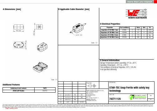
7.1 7.0 6.02012-06-272012-04-302008-01-03SStSStSMuSStSMu-Würth Elektronik eiSos GmbH & Co. KGEMC & Inductive SolutionsMax-Eyth-Str. 174638 WaldenburgGermanyTel. +49 (0) 79 42 945 - 0A Dimensions: [mm] Additional FeaturesSafety key to lock/ unkock STAR-CLIP Fixation74271 7427711D2 General Properties:Ferrite core Ferrite core Ferrite core Plastic housing Plastic housing Test cable Test cablePropertiesMaterial Initial permeability Curie temperatureColourFlammability ClassificationApplicable cable Applicable cable lengthµi T CValue 4 W 620620150Black UL94-V0AWG2690Unit°Cmm Tol.typ.typ.F Typical Impedance Characteristics:I Cautions and Warnings:The following conditions apply to all goods within the product series of WE-STAR TECof Würth Elektronik eiSos GmbH & Co. KG:General:All recommendations according to the general technical specifications of the data sheet have to be complied with.The disposal and operation of the product within ambient conditions which probably alloy or harm the component surface has to be avoided.The packaging of the product is to encase the needed humidity of the plastic housing. To ensure the humidity level, the products have to be stored in this delivered packaging. If not, the products are losing their humidity. In this case you can re-condition the components according to the internal standard WE1883 to ensure the necessary humidity in the plastic.To ensure the operating mode of the product, the ambient temperature at processing (when the part will be mounted on the cable) has to be in the range of 15 to 25 °C.Before mounting, the part should be stored for one hour in this condition.The responsibility for the applicability of customer specific products and the use in a particular customer design is always within the authority of the customer. All technical specifications for standard products do also apply for customer specific products.Direct mechanical impact to the product and the forcible closing of this shall be prevented as the ferrite material of the ferrite body or the pla-stic housing could flake or in the worst case it could break.Product specific:Follow all instructions mentioned in the datasheet, especially:•The cable diameter must be pointed out, otherwise no warranty will be sustained.•Violation of the technical product specifications such as exceeding the nominal rated current will result in the loss of warranty.1. General Customer ResponsibilitySome goods within the product range of Würth Elektronik eiSos GmbH & Co. KG contain statements regarding general suitability for certain application areas. These statements about suitability are based on our knowledge and experience of typical requirements concerning the are-as, serve as general guidance and cannot be estimated as binding statements about the suitability for a customer application. The responsibi-lity for the applicability and use in a particular customer design is always solely within the authority of the customer. Due to this fact it is up to the customer to evaluate, where appropriate to investigate and decide whether the device with the specific product characteristics described in the product specification is valid and suitable for the respective customer application or not.2. Customer Responsibility related to Specific, in particular Safety-Relevant ApplicationsIt has to be clearly pointed out that the possibility of a malfunction of electronic components or failure before the end of the usual lifetime can-not be completely eliminated in the current state of the art, even if the products are operated within the range of the specifications.In certain customer applications requiring a very high level of safety and especially in customer applications in which the malfunction or failure of an electronic component could endanger human life or health it must be ensured by most advanced technological aid of suitable design of the customer application that no injury or damage is caused to third parties in the event of malfunction or failure of an electronic component.3. Best Care and AttentionAny product-specific notes, warnings and cautions must be strictly observed.4. Customer Support for Product SpecificationsSome products within the product range may contain substances which are subject to restrictions in certain jurisdictions in order to serve spe-cific technical requirements. Necessary information is available on request. In this case the field sales engineer or the internal sales person in charge should be contacted who will be happy to support in this matter.5. Product R&DDue to constant product improvement product specifications may change from time to time. As a standard reporting procedure of the Product Change Notification (PCN) according to the JEDEC-Standard inform about minor and major changes. In case of further queries regarding the PCN, the field sales engineer or the internal sales person in charge should be contacted. The basic responsibility of the customer as per Secti-on 1 and 2 remains unaffected.6. Product Life CycleDue to technical progress and economical evaluation we also reserve the right to discontinue production and delivery of products. As a stan-dard reporting procedure of the Product Termination Notification (PTN) according to the JEDEC-Standard we will inform at an early stage about inevitable product discontinuance. According to this we cannot guarantee that all products within our product range will always be available. Therefore it needs to be verified with the field sales engineer or the internal sales person in charge about the current product availability ex-pectancy before or when the product for application design-in disposal is considered.The approach named above does not apply in the case of individual agreements deviating from the foregoing for customer-specific products.7. Property RightsAll the rights for contractual products produced by Würth Elektronik eiSos GmbH & Co. KG on the basis of ideas, development contracts as well as models or templates that are subject to copyright, patent or commercial protection supplied to the customer will remain with Würth Elektronik eiSos GmbH & Co. KG.8. General Terms and ConditionsUnless otherwise agreed in individual contracts, all orders are subject to the current version of the “General Terms and Conditions of Würth Elektronik eiSos Group”, last version available at .J Important Notes:The following conditions apply to all goods within the product range of Würth Elektronik eiSos GmbH & Co. KG:分销商库存信息: WURTH-ELECTRONICS 74271112S。
Axalta 392-9008-00 RTU 填充材料说明书
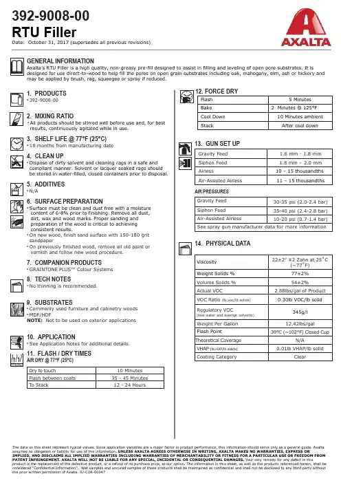
The data on this sheet represent typical values. Since application variables are a major factor in product performance, this information should serve only as a general guide. Axalta assumes no obligation or liability for use of this information. UNLESS AXALTA AGREES OTHERWISE IN WRITING, AXALTA MAKES NO WARRANTIES, EXPRESS ORIMPLIED, AND DISCLAIMS ALL IMPLIED WARRANTIES INCLUDING WARRANTIES OF MERCHANTABILITY OR FITNESS FOR A PARTICULAR USE OR FREEDOM FROM PATENT INFRINGEMENT. AXALTA WILL NOT BE LIABLE FOR ANY SPECIAL, INCIDENTAL OR CONSEQUENTIAL DAMAGES. Your only remedy for any defect in thisproduct is the replacement of the defective product, or a refund of its purchase price, at our option. The information in this sheet, as well as the products referenced herein, shall beGENERAL INFORMATIONAxalta ’s RTU Filler is a high quality, non-greasy pre-fill designed to assist in filling and leveling of open pore substrates. It isdesigned for use direct-to-wood to help fill the pores on open grain substrates including oak, mahogany, elm, ash or hickory and may be applied by brush, rag, squeegee or spray if reduced.1. PRODUCTS• 392-9008-002. MIXING RATIO• All products should be stirred well before use and, for bestresults, continuously agitated while in use.3. SHELF LIFE @ 77°F (25°C)• 18 months from manufacturing date4. CLEAN UP• Dispose of dirty solvent and cleaning rags in a safe andcompliant manner. Solvent or lacquer soaked rags should be stored in water-filled, closed containers prior to disposal.5. ADDITIVES• N/A6. SURFACE PREPARATION• Surface must be clean and dust free with a moisturecontent of 6-8% prior to finishing. Remove all dust, dirt, wax and wood marks. Proper sanding and preparation of the wood is critical to achieving consistent results.• On new wood, finish sand surface with 150-180 grit sandpaper• On previously finished wood, remove all old paint or varnish and follow new wood procedure.7. COMPANION PRODUCTS• GRAINTONE PLUS™ Colour Systems8. TECH NOTES• No thinning is recommended.9. SUBSTRATES• Commonly used furniture and cabinetry woods • MDF/HDFNOTE: Not to be used on exterior applications10. APPLICATION• See Application Notes for additional details.11. FLASH / DRY TIMESAIR DRY @ 77°F (25°C)AIR PRESSURES14.PHYSICAL DATAThe data on this sheet represent typical values. Since application variables are a major factor in product performance, this information should serve only as a general guide. Axaltaassumes no obligation or liability for use of this information. UNLESS AXALTA AGREES OTHERWISE IN WRITING, AXALTA MAKES NO WARRANTIES, EXPRESS OR IMPLIED, AND DISCLAIMS ALL IMPLIED WARRANTIES INCLUDING WARRANTIES OF MERCHANTABILITY OR FITNESS FOR A PARTICULAR USE OR FREEDOM FROM PATENT INFRINGEMENT. AXALTA WILL NOT BE LIABLE FOR ANY SPECIAL, INCIDENTAL OR CONSEQUENTIAL DAMAGES. Your only remedy for any defect in thisproduct is the replacement of the defective product, or a refund of its purchase price, at our option. The information in this sheet, as well as the products referenced herein, shall be。
FortiGate-80D 产品说明书
Multi-threat protection from a single device increases security and lowers costs Unlimited user licensing and comprehensive features Allows implementation of WAN optimization and web cache, as well as extensive internal logging and reporting.
FortiCare
Worldwide 24x7 Support
FortiGuard
Threat Research & Response
HaБайду номын сангаасdware
5
5
5
1
2
3
1 Console Port
Advanced Features
The FortiGate-80D offers beyond the industry’s best firewall with the latest in Advanced Threat Protection including Sandboxing and anti-bot protection, Feature Select Options for simplifying configurations and deployments, and Contextual Visibility for enhanced reporting and management.
2
Highlights
FortiOS — The World’s Most Advanced Security Operating System
PT4212A;PT4213A;PT4213C;PT4212C;PT4214A;中文规格书,Datasheet资料
Features•Wide Input Voltage Range: 38V to 75V•1,500 VDC Isolation • 6 Pin DIP Package •Low-Profile (8mm)•Pin-compatible with PT4200 Series •No External Components Required 2•Safety Approvals —PendingDescriptionThe PT4210 series of low-power isolated DC-DC converters are pin-compatible with Power T rends’ popular PT4200 series. The PT4210 series has improved load regulation over the PT4200, and is a compatible alternative for both new and existing designs.Applications include T elecom and Datacom systems where both board space and height are a premium.The PT4210 series is offered in both through-hole or SMD-DIP package types with single non-adjustable output voltages of 3.3V , 5V , and 12V .5-7 Watt Low-Profile Isolated DC-DC ConverterSLTS137A(Revised 4/19/2001)(2)The maximum output capacitance must not exceed 150µF for the PT4212, 120µF for the PT4213, and 47µF for the PT4214.Typical Characteristics5-7 Watt Low-ProfileIsolated DC-DC ConverterPT4210 SeriesUsing the Remote On/Off Function on thePT4210 Isolated 7W DC/DC ConvertersApplications requiring output voltage On/Off control, the PT4210 DC/DC converter series incorporates a “Remote On/Off” control (pin 11). This feature can be used when there is a requirement for the module to be switched off without removing the applied input source voltage.The converter functions normally with Pin 11 open-circuit, providing a regulated output voltage when a valid source voltage is applied to +V in (pin 18), with respect to –V in (pin 17). When a low-level 1 ground signal is applied to pin 11, the converter output will be turned off.Figure 1 shows an application schematic, which details the typical use of the Remote On/Off function. Note the discrete transistor (Q1). The control pin has its own internal pull-up, and must be controlled with an open-collector or open-drain device (See notes 2 & 3). T able 1 gives the input requirements.When placed in the “Off” state, the standby current drawn from the input source is typically reduced to less than 1mA. Table 1; Remote On/Off Control Requirements 1Parameter Min Typ MaxDisable-0.1V— 1.0VEnable 5.0V 3—Open-Circuit 2V o/c [Open-Circuit]——10VI in [pin 11 at –V in]—–100µA—Notes:1.The Remote On/Off control uses –V in (pin 17) as its groundreference. All voltages specified are with respect to –V in.e an open-collector device (preferably a discretetransistor) for the Remote On/Off input. Do not connect apull-up resistor directly to pin 11.3.The Remote On/Off pin may be controlled with devices that havea totem-pole output providing that a blocking diode isused (See Figure 1). The blocking diode is required toprevent current from being injected into On/Off control pin. Note: For TTL devices a pull-up may be required on the cathode side of the blocking diode. This is to guarantee aminimum enable voltage at pin 11 (See Figure 1).4.The PT4210 converters incorporate an “Under-VoltageLockout” (UVLO). The UVLO will keep the module off when the input voltage to the converter is low, regardless of the state of the Remote On/Off control. T able 2 gives the UVLO input voltage thresholds.Table 2; UVLO Thresholds 4Figure 1Turn-On Time: In the circuit of Figure 1, turning Q1 on applies a low-voltage to pin 11 and disables the converter output. Correspondingly, turning Q1 off allows pin 11to be pulled high by an internal pull-up resistor. The converter produces a regulated output voltage within 50ms. Although the rise-time of the output is short (<1ms), the delay time will vary depending upon the input voltage and the module’s internal timing. Figure 2 shows shows an example of the output response for a PT4213 (5.0V), following the turn-off of Q1 at time t =0. The waveform was measured with a 48Vdc input voltage, and 1.2Adc resistive load.Figure 2o-Vo +V-VinSeries V in Range UVLO ThresholdPT421038 – 75V36V ±2Vtime (milli-secs)Suffix A, C(Revised 12/1/2000)PACKAGE INFORMATION AND DIMENSIONSPACKAG PACKAGING INFORMATIONOrderable Device Status (1)Package Type PackageDrawing Pins Package Qty Eco Plan (2)Lead/Ball FinishMSL PeaPT4212A OBSOLETE DIP MODULE EGH6TBD Call TI Call TIPT4212C NRND DIP MODULE EGJ618TBD Call TI Level-1-215CPT4213A NRND DIP MODULE EGH618TBD Call TI Level-1-215CPT4213C NRND DIP MODULE EGJ618TBD Call TI Level-1-215CPT4214A OBSOLETE DIP MODULE EGH6TBD Call TI Call TIPT4214C NRND DIP MODULE EGJ618TBD Call TI Level-1-215C(1) The marketing status values are defined as follows:ACTIVE: Product device recommended for new designs.LIFEBUY: TI has announced that the device will be discontinued, and a lifetime-buy period is in effect.NRND: Not recommended for new designs. Device is in production to support existing customers, but TI does not recommend using this part in a new PREVIEW: Device has been announced but is not in production. Samples may or may not be available.OBSOLETE: TI has discontinued the production of the device.(2) Eco Plan - The planned eco-friendly classification: Pb-Free (RoHS), Pb-Free (RoHS Exempt), or Green (RoHS & no Sb/Br) - please check http://www.tinformation and additional product content details.TBD: The Pb-Free/Green conversion plan has not been defined.Pb-Free (RoHS): TI's terms "Lead-Free" or "Pb-Free" mean semiconductor products that are compatible with the current RoHS requirements for alllead not exceed 0.1% by weight in homogeneous materials. Where designed to be soldered at high temperatures, TI Pb-Free products are suitable fo Pb-Free (RoHS Exempt): This component has a RoHS exemption for either 1) lead-based flip-chip solder bumps used between the die and package, the die and leadframe. The component is otherwise considered Pb-Free (RoHS compatible) as defined above.Green (RoHS & no Sb/Br): TI defines "Green" to mean Pb-Free (RoHS compatible), and free of Bromine (Br) and Antimony (Sb) based flame retard in homogeneous material)(3) MSL, Peak Temp. -- The Moisture Sensitivity Level rating according to the JEDEC industry standard classifications, and peak solder temperature.Important Information and Disclaimer:The information provided on this page represents TI's knowledge and belief as of the date that it is provided. TIprovided by third parties, and makes no representation or warranty as to the accuracy of such information. Efforts are underway to better integrate inf continues to take reasonable steps to provide representative and accurate information but may not have conducted destructive testing or chemical an TI and TI suppliers consider certain information to be proprietary, and thus CAS numbers and other limited information may not be available for releas In no event shall TI's liability arising out of such information exceed the total purchase price of the TI part(s) at issue in this document sold by TI to Cu /IMPORTANT NOTICETexas Instruments Incorporated and its subsidiaries(TI)reserve the right to make corrections,enhancements,improvements and other changes to its semiconductor products and services per JESD46C and to discontinue any product or service per JESD48B.Buyers should obtain the latest relevant information before placing orders and should verify that such information is current and complete.All semiconductor products(also referred to herein as“components”)are sold subject to TI’s terms and conditions of sale supplied at the time of order acknowledgment.TI warrants performance of its components to the specifications applicable at the time of sale,in accordance with the warranty in TI’s terms and conditions of sale of semiconductor products.Testing and other quality control techniques are used to the extent TI deems necessary to support this warranty.Except where mandated by applicable law,testing of all parameters of each component is not necessarily performed.TI assumes no liability for applications assistance or the design of Buyers’products.Buyers are responsible for their products and applications using TI components.To minimize the risks associated with Buyers’products and applications,Buyers should provide adequate design and operating safeguards.TI does not warrant or represent that any license,either express or implied,is granted under any patent right,copyright,mask work right,or other intellectual property right relating to any combination,machine,or process in which TI components or services are rmation published by TI regarding third-party products or services does not constitute a license to use such products or services or a warranty or endorsement e of such information may require a license from a third party under the patents or other intellectual property of the third party,or a license from TI under the patents or other intellectual property of TI.Reproduction of significant portions of TI information in TI data books or data sheets is permissible only if reproduction is without alteration and is accompanied by all associated warranties,conditions,limitations,and notices.TI is not responsible or liable for such altered rmation of third parties may be subject to additional restrictions.Resale of TI components or services with statements different from or beyond the parameters stated by TI for that component or service voids all express and any implied warranties for the associated TI component or service and is an unfair and deceptive business practice. TI is not responsible or liable for any such statements.Buyer acknowledges and agrees that it is solely responsible for compliance with all legal,regulatory and safety-related requirements concerning its products,and any use of TI components in its applications,notwithstanding any applications-related information or support that may be provided by TI.Buyer represents and agrees that it has all the necessary expertise to create and implement safeguards which anticipate dangerous consequences of failures,monitor failures and their consequences,lessen the likelihood of failures that might cause harm and take appropriate remedial actions.Buyer will fully indemnify TI and its representatives against any damages arising out of the use of any TI components in safety-critical applications.In some cases,TI components may be promoted specifically to facilitate safety-related applications.With such components,TI’s goal is to help enable customers to design and create their own end-product solutions that meet applicable functional safety standards and requirements.Nonetheless,such components are subject to these terms.No TI components are authorized for use in FDA Class III(or similar life-critical medical equipment)unless authorized officers of the parties have executed a special agreement specifically governing such use.Only those TI components which TI has specifically designated as military grade or“enhanced plastic”are designed and intended for use in military/aerospace applications or environments.Buyer acknowledges and agrees that any military or aerospace use of TI components which have not been so designated is solely at the Buyer's risk,and that Buyer is solely responsible for compliance with all legal and regulatory requirements in connection with such use.TI has specifically designated certain components which meet ISO/TS16949requirements,mainly for automotive ponents which have not been so designated are neither designed nor intended for automotive use;and TI will not be responsible for any failure of such components to meet such requirements.Products ApplicationsAudio /audio Automotive and Transportation /automotiveAmplifiers Communications and Telecom /communicationsData Converters Computers and Peripherals /computersDLP®Products Consumer Electronics /consumer-appsDSP Energy and Lighting /energyClocks and Timers /clocks Industrial /industrialInterface Medical /medicalLogic Security /securityPower Mgmt Space,Avionics and Defense /space-avionics-defense Microcontrollers Video and Imaging /videoRFID OMAP Mobile Processors /omap TI E2E Community Wireless Connectivity /wirelessconnectivityMailing Address:Texas Instruments,Post Office Box655303,Dallas,Texas75265Copyright©2012,Texas Instruments Incorporated分销商库存信息:TIPT4212A PT4213A PT4213C PT4212C PT4214A PT4214C。
LC860EQN-FJA1(1)(1)
Title86.0” QWUXGA TFT LCDBUYERMODELSUPPLIER LG Display Co., Ltd. *MODEL LC860EQNSUFFIXFJA1 (RoHS Verified)SPECIFICATIONFOR APPROVALAPPROVED BYSIGNATUREDATEHongsung Song / Team LeaderREVIEWED BYBooYoung Kim / Project LeaderPREPARED BYByoungson Ryu / EngineerTV Product Development Dept.LG Display Co., Ltd.APPROVED BYSIGNATUREDATE///Please return 1 copy for your confirmation withyour signature and comments.( ● ) Preliminary Specification () Final SpecificationCONTENTSNumber ITEM Page COVER -CONTENTS 1RECORD OF REVISIONS 21 GENERAL DESCRIPTION 32 ABSOLUTE MAXIMUM RATINGS 43 ELECTRICAL SPECIFICATIONS 53-1 ELECTRICAL CHARACTERISTICS 5 3-2 INTERFACE CONNECTIONS 7 3-3 SIGNAL TIMING SPECIFICATIONS 11 3-4 V by One SIGNAL SPECIFICATIONS 12 3-5 COLOR DATA REFERENCE 14 3-6 POWER SEQUENCE 154 OPTICAL SPECIFICATIONS 165 MECHANICAL CHARACTERISTICS 206 RELIABILITY 237 INTERNATIONAL STANDARDS 247-1 SAFETY 24 7-2 ENVIRONMENT 24 8 PACKING 258-1 INFORMATION OF LCM LABEL 25 8-2 PACKING FORM 25 9 PRECAUTIONS 26 9-1 MOUNTING PRECAUTIONS26 9-2 OPERATING PRECAUTIONS26 9-3 ELECTROSTATIC DISCHARGE CONTROL26 9-4 PRECAUTIONS FOR STRONG LIGHT EXPOSURE26 9-5 STORAGE26 9-6 APPROPRIATE CONDITION FOR COMMERCIAL DISPLAY 27RECORD OF REVISIONSRevision No. Revision Date Page Description0.1 Nov, 10, 2015 - Preliminary Specification (First Draft)Active Screen Size 85.60 inches(2174.27 mm) diagonal Outline Dimension 1922.2 (H) × 1093.2 (V) X 13.6 (B) (Typ.) Pixel Pitch 0.4935 mm x 0.4935 mmPixel Format 3840 horiz. by 2160 vert. Pixels, RGB stripe arrangement Color Depth 10bit(D), 1.07Billon colors Luminance, White 410 cd/m 2 (Center 1point ,Typ.)Viewing Angle (CR>10) Viewing angle free ( R/L 178 (Min.), U/D 178 (Min.))Power Consumption Total 260.72 W (Typ.) [Logic= 31.92 W, LED Driver= 228.8 W (ExtVbr_B=100%) Weight 38.0 (TBD) Kg (Typ.)Display Mode Transmissive mode, Normally blackSurface TreatmentHard coating(2H), Anti-glare low reflection treatment of the front polarizer (Haze 3%(Typ.))1. General DescriptionThe LC860EQN is a Color Active Matrix Liquid Crystal Display with an integral Light Emitting Diode (LED) backlight system. The matrix employs a-Si Thin Film Transistor as the active element.It is a transmissive display type which is operating in the normally black mode. It has a 85.60 inch diagonally measured active display area with QWUXGA resolution (2160 vertical by 3840 horizontal pixel array). Each pixel is divided into Red, Green and Blue sub-pixels or dots which are arrayed in vertical stripes.Gray scale or the luminance of the sub-pixel color is determined with a 10-bit gray scale signal for each dot. Therefore, it can present a palette of more than 1.07Bilion colors. It has been designed to apply the 10-bit 8 Lane V by One interface.It is intended to support LCD TV, PCTV where high brightness, super wide viewing angle, high color gamut, high color depth and fast response time are important.Source Driver CircuitTFT - LCD Panel(3840 × RGB × 2160 pixels)G1S1S3840G2160EPI (RGB)Timing ControllerVby1 Rx +L/D + DGA + ODCEEPROM Power CircuitBlockSDASCLData formatCN2(51pin) Vby1 8lane +12.0V Control Signals Power SignalsOption signal I2CVby1 1~8laneEPI (RGB)CN1 5pin)+12.0VBitselection HTPDN LOCKNL-DIM Enable Local Dimming : 24 BlockLED Driver+24.0V, GND, On/Off ExtV BR-BVSYNC, SIN, SCLK, GNDThe following items are maximum values which, if exceeded, may cause faulty operation or permanent damage to the LCD module.2. Absolute Maximum RatingsTable 1. ABSOLUTE MAXIMUM RATINGS1. Ambient temperature condition (Ta = 25 2 °C )2. Temperature and relative humidity range are shown in the figure below. Wet bulb temperature should be Max 39°C, and no condensation of water.3. Gravity mura can be guaranteed below 40°C condition.4. The maximum operating temperatures is based on the test condition that the surface temperatureof display area is less than or equal to 68°C with LCD module alone in a temperature controlled chamber. Thermal management should be considered in final product design to prevent the surface temperature of display area from being over 68℃. The range of operating temperature may be degraded in case of improper thermal management in final product design.NoteParameterSymbol Value Unit NoteMin Max Power Input Voltage LCD Circuit V LCD -0.3 +14.0 V DC 1 Driver Control VoltageON/OFF V OFF / V ON -0.3 +3.9 V DC BrightnessEXTV BR-B 0.0 +3.9 V DC T-Con Option Selection Voltage V LOGIC -0.3 +4.0 V DC Operating Temperature T OP 0 +50 °C 2,3 Storage Temperature T ST -20 +60 °C Panel Front Temperature T SUR - +68 °C 4 Operating Ambient Humidity H OP 10 90 %RH 2,3 Storage HumidityH ST590%RH90%1020304050607080-20 010 20 30 4050 Dry Bulb Temperature [°C ]Wet BulbTemperature [°C ]StorageOperationH u m i d i t y [(%)R H ]10% 40%60%605%3. Electrical Specifications3-1. Electrical CharacteristicsIt requires two power inputs. One is employed to power for the LCD circuit. The other Is used for the LED backlight and LED Driver circuit.Table 2. ELECTRICAL CHARACTERISTICSParameter SymbolValueUnit notes Min Typ MaxCircuit :Power Input Voltage V LCD 10.8 12.0 13.2 V DCPower Input Current I LCD - 2660(TBD) 3458(TBD) mA 1 - 4380(TBD) 5694(TBD) mA 2T-CON OptionSelection Voltage Input High Voltage V IH 2.7 - 3.6 V DC Input Low Voltage V IL0 - 0.7 V DCPower Consumption P LCD - 31.9(TBD) 41.5(TBD) Watt 1 Rush current I RUSH - - 12.0 A 3notes1. The specified current and power consumption are under the V LCD=12.0V, Ta=25 2°C, f V=120Hz condition, and mosaic pattern(8 x 6) is displayed and f V is the frame frequency.2. The current is specified at the maximum current pattern.3. The duration of rush current is about 2ms and rising time of power input is 0.5ms (min.).4. Ripple voltage level is recommended under ±5% of typical voltageMosaic Pattern(8 x 6) Max Current Pattern (Full White Pattern)Table 3. ELECTRICAL CHARACTERISTICS (Continue)Available duty rangeHighLow0%1%99% 100%Ext_PWM Input DutyParameterSymbolValuesUnitNotesMinTypMaxLED Driver :Power Supply Input Voltage VBL 21.6 24.0 26.4 Vdc 1 Power Supply Input Current IBL-9.5 (TBD) (TBD)A1Power Supply Input Current (In-Rush)In-rush - - (TBD) AVBL = 21.6V ExtVBR-B=100%3Power Consumption (Total)PBL - 228.8 (TBD) (TBD) W 1Input Voltage for Control System SignalsOn/OffOnV on2.5-3.6VdcOffV off -0.3 0.0 0.7 Vdc Brightness Adjust ExtVBR-B 1- 100% On Duty5PWM Frequency for NTSC & PAL PAL 100 Hz 2 NTSC 120 Hz 2Pulse Duty Level (PWM)HighLevel 2.5 - 3.6 Vdc HIGH : on duty LOW : off dutyLow Level0.0 -0.7 VdcLED : Life Time30,00050,000Hrs6Notes :1. Electrical characteristics are determined after the unit has been ‘ON’ and stable for approximately 60minutes at 25±2°C. The specified current and power consumption are under the typical supply Input voltage 24Vand V BR (Ext V BR-B : 100%), it is total power consumption.2. LGD recommend that the PWM freq. is synchronized with One time harmonic of V_sync signal of system. Though PWM frequency is over 120Hz (max 252Hz), function of LED Driver is not affected.3. The duration of rush current is about 200ms. This duration is applied to LED on time4. Even though inrush current is over the specified value, there is no problem if I 2T spec of fuse is satisfied.5. Ext_PWM Signal have to input available duty range.Between 99% and 100% ExtVBR-B duty have to be avoided. ( 99% < ExtVBR-B < 100%) But ExtVBR-B 0% and 100% is possible.6. The life time is determined as the time at which brightness of the LED is 50% compared to that of initial value at the typical LED current on condition of continuous operating at 25 2°C, based on duty 100%.3-2. Interface ConnectionsThis LCD module employs theree kinds of interface connection, 5-pin connector, 51-pin connectorand 41-pin connector are used for the module electronics and 14-pin,12-pin connector is used for the integral backlight system.3-2-1. LCD Module- LCD Connector(CN1): 20037WR-H05 (manufactured by YEONHO)Table 4-1. MODULE CONNECTOR(CN1) PIN CONFIGURATIONNo Symbol Description1 GND Ground2 GND Ground3 VLCD Power Supply +12.0V4 VLCD Power Supply +12.0V5 VLCD Power Supply +12.0VTable 4-2. MODULE CONNECTOR(CN2) PIN CONFIGURATION- LCD Connector(CN1): FI-RXE51S-HF (manufactured by JAE) or compatible or GT05S-51S-H38 (manufactured by LSM) or IS050-C51B-C39-C(manufactured by UJU) notes NoSymbol DescriptionNoSymbol Description1 NC No Connection(notes 2) 27 GND Ground2 NC No Connection(notes 2) 28 Rx0n V-by-One HS Data Lane 03 NC No Connection(notes 2) 29 Rx0p V-by-One HS Data Lane 04 NC No Connection(notes 2) 30 GND Ground5 NC No Connection(notes 2) 31 Rx1n V-by-One HS Data Lane 16 NC No Connection(notes 2) 32 Rx1p V-by-One HS Data Lane 17 NC No Connection(notes 2) 33 GND Ground8 NC No Connection(notes 2) 34 Rx2n V-by-One HS Data Lane 2 9 NC No Connection 35 Rx2p V-by-One HS Data Lane 2 10 GND Ground 36 GND Ground11 GND Ground 37 Rx3n V-by-One HS Data Lane 3 12 GND Ground 38 Rx3p V-by-One HS Data Lane 3 13 GND Ground39 GND Ground14 NC NO CONNECTION 40 Rx4n V-by-One HS Data Lane 4 15 NC NO CONNECTION 41 Rx4p V-by-One HS Data Lane 4 16NCNO CONNECTION42 GNDGround17Input Mode Vx1 Input Data Format'L'=Non-Division , 'H'=2-Division 43 Rx5n V-by-One HS Data Lane 5 18 SDA SDA 44 Rx5p V-by-One HS Data Lane 5 19 SCL SCL45 GND Ground20 WP Write Protection 46 Rx6n V-by-One HS Data Lane 6 21Bit_SEL ‘H’ = 10bit , ‘L’ = 8bit47 Rx6p V-by-One HS Data Lane 6 22 LOCAL_ONH’ = Enable , ‘L’ or NC = Disable 48 GND Ground23RBF ‘H’ : AGP(Default),‘L’ : NSB (No signal Black) 49 Rx7n V-by-One HS Data Lane 7 24 GND Ground50 Rx7p V-by-One HS Data Lane 7 25 HTPDN Hot plug detect 51 GNDGround26LOCKNLock detect---1. All GND (ground) pins should be connected together to the LCD module’s metal frame.2. #1~#8 NC (No connection ) : These pins are used for back up power source, V LCD (power input) . These pins are should be connected together.3. All Input levels of V-by-One signals are based on the V-by-One HS Standard Version 1.4. 4. #18 & #19, #20 NC (No Connection) : These pins are used only for LGD (Do not connect)5. Specific pin (#22) is used for Local Dimming function of the LCD module.If not used, these pins are no connection. (Please see the Appendix IV-2 for more information.) 6. About specific pin (#17) , Please see the Appendix VI .7. Specific pin No. #23 is used for “No signal detection” of system signal interface.It should be GND for NSB (No Signal Black) while the system interface signal is not. If this pin is “H” or “NC”, LCD Module displays AGP (Auto Generation Pattern).8. Specific pin (pin No. #18, #19 ,#20) is used for Controlling Local Dimming register in the LCM Module .CN2#1#51Rear view of LCM#1#51CN2#1#5CN1#1CN1#53-2-2. Backlight Module Table 5-1. LED DRIVER CONNECTOR PIN CONFIGURATION◆ Rear view of LCM◆Statusnotes : 1. GND should be connected to the LCD module’s metal frame. 2. Normal : Low (under 0.7V) / Abnormal : Open3. High : on duty / Low : off duty, Pin#14 can be opened. ( if Pin #14 is open , EXTVBR-B is 100% )4. Each impedance of pin #12 and 14 is over 50 [K Ω] .Pin No Symbol Description (CN_A1)Description (CN_A2)Note1 VBL Power Supply +24.0V Power Supply +24.0V2 VBL Power Supply +24.0V Power Supply +24.0V3 VBL Power Supply +24.0V Power Supply +24.0V4 VBL Power Supply +24.0V Power Supply +24.0V5 VBL Power Supply +24.0V Power Supply +24.0V6 GND Backlight Ground Backlight Ground 17 GND Backlight Ground Backlight Ground8 GND Backlight Ground Backlight Ground9 GND Backlight Ground Backlight Ground 10 GND Backlight Ground Backlight Ground 11 Status Backlight StatusDon’t care 2 12 VON/OFFBacklight ON/OFF control Don’t care13 NC Don’t care 14EXTVBR_BExternal PWM3Board A 112 114CN_A2CN_A1… …121141Master-LED Driver Connector: 20022WR - H14B2(Yeonho) or compatible, 20022WR-H12B2(Yeonho) or compatible - Mating Connector: 20022HS-H14B2(Yeonho) or compatible, 20022HS-H12B2(Yeonho) or compatible3-3. Signal Timing SpecificationsTable 6 shows the signal timing required at the input of the Vx1 transmitter. All of the interface signal timings should be satisfied with the following specification for normal operation. Table 6. TIMING TABLE (DE Only Mode)notes: 1. The input of HSYNC & VSYNC signal does not have an effect on normal operation (DE Only Mode). If you use spread spectrum of EMI, add some additional clock to minimum value for clock margin.2. The performance of the electro-optical characteristics may be influenced by variance of the vertical refresh rate and the horizontal frequency3. Spread Spectrum Rate (SSR) is limited to ±0.5% center spread at 30KHz※ Timing should be set based on clock frequency.ITEMSymbolMin Typ Max UnitNote HorizontalDisplay Periodt HV 480 480 480 t CLK 3840/8 Blank t HB 60 70 120 t CLK 1Total t HP 540 550 600 t CLKVerticalDisplay Periodt VV 2160 2160 2160 Lines Blank t VB 40 90 600 Lines 1Totalt VP220022502760LinesITEMSymbol Min Typ Max Unit Note FrequencyDCLKf CLK 67 74.25 78.00 MHz 594/8 Horizontal f H 121.8 135 140 KHz 2 Verticalf V476063Hz23-4-1. V by One Input Signal Timing DiagramABF EDCㆍ ㆍ ㆍ ㆍㆍ ㆍ Y=0mVX=0 UI X=1 UI1UI = 1/(Serial data rate)YXX[UI]NoteY[mV]NoteA 0.25 (max) 2 0 -B 0.3 (max) 2 50 3C 0.7(min) 3 50 3D 0.75(min) 3 0 -E 0.7(min) 3 l -50 l 3 F0.3(max)2l -50 l3Table7. Eye Mask Specification3-4. V by One input signal Characteristicsnotes 1. All Input levels of V by One signals are based on the V by One HS Standard Ver. 1.4 2. This is allowable maximum value. 3. This is allowable minimum value.4. The eye diagram is measured by the oscilloscope and receiver CDR characteristic must be emulated.- PLL bandwidth : 15 Mhz - Damping Factor : 1<TCON – VbyOne Brief Diagram >3-4-2. V by One Input Signal CharacteristicstRISK_INTERLane0Lane1 Vdiff =0Vdiff =0DescriptionSymbol Min Max Unit notes Allowable inter-pair skew between lanes tRISK_INTER - 5 UI 1,3 Allowable iner-pair skew between sub-blockstRISK_BLOCK-1DE1,4<Inter-pair Skew between two Lanes> <Inter-pair Skew between two sub Blocks>Notes 1.1UI = 1/serial data rate2. it is the time difference between the true and complementary single-ended signals.3. it is the time difference of the differential voltage between any two lanes in one sub block.4. it is the time difference of the differential voltage between any two blocks in one IP.Rx1Vblank HblankRx2VblankDEMax 1 DEDE1H T-CONV By One Rx IPRx8 Lane3-5. Color Data ReferenceThe brightness of each primary color (red, green, blue) is based on the 10bit or 8bit gray scale data input for the color. The higher binary input, the brighter the color. Table 8 provides a reference for color versus data input.Table 8. COLOR DATA REFERENCEPacker input & Unpacker output 30bpp RGB (10bit) 24bpp RGB (8bit)Byte0 D[0] R[2] R[0] D[1] R[3] R[1] D[2] R[4] R[2] D[3] R[5] R[3] D[4] R[6] R[4] D[5] R[7] R[5] D[6] R[8] R[6] D[7] R[9] R[7]Byte1D[8] G[2] G[0] D[9] G[3] G[1] D[10] G[4] G[2] D[11] G[5] G[3] D[12] G[6] G[4] D[13] G[7] G[5] D[14] G[8] G[6] D[15] G[9] G[7]Byte2 D[16] B[2] B[0] D[17] B[3] B[1] D[18] B[4] B[2] D[19] B[5] B[3] D[20] B[6] B[4] D[21] B[7] B[5] D[22] B[8] B[6] D[23] B[9] B[7]Byte3 D[24] Don’t care D[25] Don’t care D[26] B[0]D[27] B[1]D[28] G[0] D[29] G[1] D[30] R[0]D[31] R[1]Notes 1. 30bpp RGB (10bit) is 4 byte mode, otherwise (24bpp RGB) 3byte modeNote :3-6. Power Sequence3-6-1. LCD Driving circuit10% 0V90%10%T 1T 2T 5LED ONT 3 T 4T 6Interface Signal (Tx_clock)Power for LEDPower Supply For LCD V LCDUser Control Signal(DATA FORMAT, BIT_SEL, L-DIM EN)0VVx1 Data100%10%90% T7T 8Vx1 Lock , HTPDN (Pull-up)ParameterValueUnitNoteMinTyp Max T 1 0.5 - 20 ms 1 T 2 0 - - ms 2 T 3 400 - - ms 3 T 4 100 - - ms 3 T 51.0--s4T 6 0 - T2 ms 5 T 7 0 - - ms 6T 8--ms1. Even though T1 is over the specified value, there is no problem if I2T spec of fuse is satisfied.2. If T2 is satisfied with specification after removing LVDS Cable, there is no problem.3. The T3 / T4 is recommended value, the case when failed to meet a minimum specification, abnormal display would be shown. There is no reliability problem.4. T5 should be measured after the Module has been fully discharged between power off and on period.5. If the on time of signals (Interface signal and user control signals) precedes the on time of Power (V LCD ), it will be happened abnormal display. When T6 is NC status, T6 doesn’t need to be measured.6. It is recommendation specification that T7 has to be 0ms as a minimum value. ※ Please avoid floating state of interface signal at invalid period.※ When the power supply for LCD (VLCD) is off, be sure to pull down the valid and invalid data to 0V.LCD ModuleOptical Stage(x,y)Pritchard 880 orequivalent50cmFIG. 1 Optical Characteristic Measurement Equipment and Method4. Optical SpecificationOptical characteristics are determined after the unit has been ‘ON’ and stable in a dark environment at 25±2°C. The values are specified at distance 50cm from the LCD surface at a viewing angle of Φ and θ equal to 0 °. FIG. 1 shows additional information concerning the measurement equipment and method.Parameter SymbolValueUnit notesMin Typ MaxContrast Ratio CR 900 1200 - 1Surface Luminance, white LWH- 328 410 cd/m2 2Luminance Variation δWHITE9P 60 % 3Response TimeGray-to-Gray G to G - 8 12 ms 4Uniformity δG TO G - - 1 5Color Coordinates[CIE1931]REDRxTyp-0.030.648(TBD)Typ+0.03Ry 0.332(TBD)GREENGx 0.309(TBD)Gy 0.604(TBD)BLUEBx 0.153(TBD)By 0.053(TBD)WHITEWx 0.281Wy 0.288Color Temperature 10,000 KColor Gamut (NTSC) 72 %Viewing Angle (CR>10)x axis, right(φ=0°) θr (x axis) 89 - -degree 6 x axis, left (φ=180°) θl (x axis) 89 - -y axis, up (φ=90°) θu (y axis) 89 - -y axis, down (φ=270°) θd (y axis) 89 - -Gray Scale - - - 7 Table 11. OPTICAL CHARACTERISTICSTa= 25±2°C, V LCD=12.0V, f V=60Hz, Dclk=74.25MHz,EXTV BR-B =100%Table 11. GRAY SCALE SPECIFICATIONGray LevelLuminance [%] (Typ)L0 0.083 L63 0.27 L127 1.04 L191 2.49 L255 4.68 L319 7.66 L383 11.5 L447 16.1 L511 21.6 L575 28.1 L639 35.4 L703 43.7 L767 53.0 L831 63.2 L895 74.5 L959 86.7 L1023100notes : 1. Contrast Ratio(CR) is defined mathematically as :Surface Luminance with all white pixels Contrast Ratio =Surface Luminance with all black pixels It is measured at center 1-point.2. Surface luminance is determined after the unit has been ‘ON’ and 1 Hour after lighting thebacklight in a dark environment at 25±2°C. Surface luminance is the luminance value at center 1-point across the LCD surface 50cm from the surface with all pixels displaying white. For more information see the FIG. 23. The variation in surface luminance , WHITE is defined as :WHITE(9P) = Minimum (Lon1,Lon2~ Lon8, Lon9) / Maximum (Lon1,Lon2~ Lon8, Lon9)*100 Where Lon1 to Lon9 are the luminance with all pixels displaying white at 9 locations For more information, see the FIG. 2.4. Response time is the time required for the display to transit from G(N) to G(M) (Rise Time, Tr R ) and from G(M) to G(N) (Decay Time, Tr D ). For additional information see the FIG. 3. (N<M) ※ G to G Spec stands for average value of all measured points. Photo Detector : RD-80S / Field : 2˚※. Gray to Gray Response time uniformity is Reference data. Appendix V5. Viewing angle is the angle at which the contrast ratio is greater than 10. The angles are determined for the horizontal or x axis and the vertical or y axis with respect to the z axis which is normal to the LCD module surface. For more information, see the FIG. 4.6. Gray scale specification Gamma Value is approximately 2.2. For more information, see the Table 12.FIG. 3 Response TimeResponse time is defined as the following figure and shall be measured by switching the input signal for “Gray(N)” and “Gray(M)”.Measuring point for surface luminance & measuring point for luminance variation.Gray(M)Gray(N)T r RT r D100 9010 0Optical ResponseN,M = Black~White, N<MGray(N)A : H / 9 mmB : V / 9 mm@ H,V : Active AreaHAVB①②③ ④⑦ ⑧ ⑨⑤ ⑥H / 2V / 2FIG. 4 Viewing AngleDimension of viewing angle rangeNormalYEφθφ = 0︒, Rightφ = 180︒, Lef tφ = 270︒, Downφ = 90︒, UpTable 13 provides general mechanical characteristics.5. Mechanical CharacteristicsTable 13. MECHANICAL CHARACTERISTICSnotes : Please refer to a mechanical drawing in terms of tolerance at the next page.ItemValueOutline DimensionHorizontal1922.2 mm Vertical 1093.2 mm Depth 13.6 mm Bezel AreaHorizontal1897.0 mmVertical 1068.0 mm Active Display AreaHorizontal1895.04 mmVertical1065.96 mm Weight 38.0(TBD)Kg (Typ.), 39.9(TBD)Kg (Max.) Case TopMaterial EGI Case Top ColorBlack LG Logo Color None Ultra HD Logo ColorNone[ FRONT VIEW ]Date VersionSET : TOP SET : DOWN[ REAR VIEW ]SET : TOPSET : DOWN6. ReliabilityTable 14. ENVIRONMENT TEST CONDITIONNo. Test Item Condition1 High temperature storage test Ta= 60°C 90% 240h2 Low temperature storage test Ta= -20°C 240h3 High temperature operation test Ta= 50°C 50%RH 500h4 Low temperature operation test Ta= 0°C 500h5 Humidity condition Operation Ta= 40 °C ,90%RH6 Altitude operatingstorage / shipment0 - 16,400 ft0 - 40,000 ft7 Vibration test(non-operating)Wave form : RandomVibration Level 0.5 GrmsBandwidth : 10 ~ 300HzDuration : X, Y, ZEach direction Per 10min8 Panel Push Test (Module Condition) Max 6kgfNote : 1. Before and after Reliability test, LCM should be operated with normal function.7. International Standards7-1. Safetya) UL 60065, Underwriters Laboratories Inc.Audio, Video and Similar Electronic Apparatus - Safety Requirements.b) CAN/CSA C22.2 No.60065:03, Canadian Standards Association.Audio, Video and Similar Electronic Apparatus - Safety Requirements.c) EN 60065, European Committee for Electrotechnical Standardization (CENELEC).Audio, Video and Similar Electronic Apparatus - Safety Requirements.d) IEC 60065, The International Electro technical Commission (IEC).Audio, Video and Similar Electronic Apparatus - Safety Requirements.7-2. Environmenta) RoHS, Directive 2011/65/EU of the European Parliament and of the council of 8 June 20118-2. Packing Forma) Lot MarkABCDEFGHIJKLMNote1. YEARb) Location of Lot Mark2. MONTHSerial NO. is printed on the label. The label is attached to the backside of the LCD module. This is subject to change without prior notice.8. PackingA,B,C : SIZE(INCH) D : YEARE : MONTHF ~ M : SERIAL NO.8-1. Information of LCM LabelMarkYear K2020 F2016 G2017 H2018 J2019 D2014 E2015 CBA2013 2012 2011 BNov MarkMonth AOct 6Jun 7Jul 8Aug 9Sep 4Apr 5May C321Dec Mar Feb Jan a) Package quantity in one Pallet : 6 pcsb) Pallet Size : 2280 mm(W) X 780 mm(D) X 1420 mm(H)9. PrecautionsPlease pay attention to the followings when you use this TFT LCD module.9-1. Mounting Precautions(1) You must mount a module using specified mounting holes (Details refer to the drawings).(2) You should consider the mounting structure so that uneven force (ex. Twisted stress, Concentrated stress) is not applied to the module. And the case on which a module is mounted should have sufficient strength so that external force is not transmitted directly to the module.(3) Please attach the surface transparent protective plate to the surface in order to protect the polarizer.Transparent protective plate should have sufficient strength in order to the resist external force.(4) You should adopt radiation structure to satisfy the temperature specification.(5) Acetic acid type and chlorine type materials for the cover case are not desirable because the formergenerates corrosive gas of attacking the polarizer at high temperature and the latter causes circuit break by electro-chemical reaction.(6) Do not touch, push or rub the exposed polarizers with glass, tweezers or anything harder than HBpencil lead. And please do not rub with dust clothes with chemical treatment.Do not touch the surface of polarizer for bare hand or greasy cloth.(Some cosmetics are detrimentalto the polarizer.)(7) When the surface becomes dusty, please wipe gently with absorbent cotton or other soft materials likechamois soaks with petroleum benzine. Normal-hexane is recommended for cleaning the adhesivesused to attach front / rear polarizers. Do not use acetone, toluene and alcohol because they causechemical damage to the polarizer(8) Wipe off saliva or water drops as soon as possible. Their long time contact with polarizer causesdeformations and color fading.(9) Do not open the case because inside circuits do not have sufficient strength.(10) Touching the LED Driver might cause an electric shock and damage to LED Driver. Please always useantistatic tools when handling the LED Driver9-2. Operating Precautions(1) Response time depends on the temperature.(In lower temperature, it becomes longer.)(2) Brightness depends on the temperature. (In lower temperature, it becomes lower.)And in lower temperature, response time(required time that brightness is stable after turned on) becomes longer(3) Be careful for condensation at sudden temperature change.Condensation makes damage to polarizer orelectrical contacted parts. And after fading condensation, smear or spot will occur.(4) When fixed patterns are displayed for a long time, remnant image is likely to occur.(5) Module has high frequency circuits. Sufficient suppression to the electromagnetic interference shall be done by system manufacturers. Grounding and shielding methods may be important to minimized the interference.(6) Please do not give any mechanical and/or acoustical impact to LCM. Otherwise, LCM can’t be operated its full characteristics perfectly.(7) A screw which is fastened up the steels should be a machine screw.(if not, it can causes conductive particles and deal LCM a fatal blow)(8) Please do not set LCD on its edge.(9) The conductive material and signal cables are kept away from LED driver inductor to prevent abnormaldisplay, sound noise and temperature rising.。
6-port 双频扇形天线(2x 698-960MHz 和 4x 1710-2690MHz)说明书
6-port sector antenna, 2x 698–960 and 4x 1710–2690 MHz, 65°HPBW, 3x RET with manual override.Integrated Internal Remote Electrical Tilt (RET), with independent control of electrical tilt withmanual override on all arraysOBSOLETEThis product was discontinued on: March 27, 2020General SpecificationsAntenna Type SectorBand MultibandGrounding Type RF connector inner conductor and body grounded to reflector andmounting bracketPerformance Note Outdoor usageRadome Material ASA, UV stabilizedRadiator Material Brass | Low loss circuit boardReflector Material AluminumRF Connector Interface7-16 DIN FemaleRF Connector Location BottomRF Connector Quantity, high band4RF Connector Quantity, low band2RF Connector Quantity, total6Remote Electrical Tilt (RET) InformationRET Interface8-pin DIN Female | 8-pin DIN MaleRET Interface, quantity 3 female | 3 maleInput Voltage10–30 VdcInternal RET High band (2) | Low band (1)Power Consumption, idle state, maximum 2 WPower Consumption, normal conditions, maximum13 WProtocol3GPP/AISG 2.0 (Single RET)16Page ofPage of 26DimensionsWidth 353 mm | 13.898 in Depth 209 mm | 8.228 in Length2065 mm | 81.299 in Net Weight, without mounting kit28 kg | 61.729 lbArray LayoutElectrical SpecificationsImpedance50 ohmOperating Frequency Band 1710 – 2690 MHz | 698 – 960 MHz Polarization±45°Electrical SpecificationsFrequency Band, MHz698–790790–890890–9601710–19201920–21702300–2690 Gain, dBi15.315.516.11818.419.2 Beamwidth, Horizontal,degrees68.268.8636263.362 Beamwidth, Vertical, degrees12.41110.1 5.8 5.1 4.2Beam Tilt, degrees0–100–100–100–100–100–10 USLS (First Lobe), dB181818181814Null Fill, dB-22-22-22-22-22-22Front-to-Back Ratio at 180°,dB252425293331CPR at Boresight, dB171212191615CPR at Sector, dB109.697.1 5.34 Isolation, Cross Polarization,dB252525252525 Isolation, Inter-band, dB303030303030VSWR | Return loss, dB 1.43 | 15.0 1.43 | 15.0 1.43 | 15.0 1.5 | 14.0 1.5 | 14.0 1.5 | 14.0 PIM, 3rd Order, 2 x 20 W, dBc-150-150-150-150-150-150Input Power per Port,maximum, watts300300300250250250 Electrical Specifications, BASTAFrequency Band, MHz698–790790–890890–9601710–19201920–21702300–2690 Gain by all Beam Tilts,average, dBi14.815.115.717.618.118.6Gain by all Beam TiltsTolerance, dB±0.2±0.2±0.2±0.6±0.3±0.6Gain by Beam Tilt, average, dBi 0 ° | 14.95 ° | 14.810 ° | 14.70 ° | 15.15 ° | 15.110 ° | 15.00 ° | 15.75 ° | 15.710 ° | 15.60 ° | 17.65 ° | 17.610 ° | 17.60 ° | 18.05 ° | 18.010 ° | 18.10 ° | 18.65 ° | 18.710 ° | 18.3Beamwidth, HorizontalTolerance, degrees±1.2±2±1.7±2.8±5.4±6.6Beamwidth, VerticalTolerance, degrees±0.8±0.6±0.4±0.3±0.4±0.3USLS, beampeak to 20° abovebeampeak, dB181818181818Front-to-Back Total Power at180° ± 30°, dB25.323.123.623.424.925.4CPR at Boresight, dB16131319181811108755Page of36CPR at Sector, dB11108755 Mechanical SpecificationsWind Loading @ Velocity, frontal926.0 N @ 150 km/h (208.2 lbf @ 150 km/h)Wind Loading @ Velocity, lateral355.0 N @ 150 km/h (79.8 lbf @ 150 km/h)Wind Loading @ Velocity, rear951.0 N @ 150 km/h (213.8 lbf @ 150 km/h)Wind Speed, maximum250 km/h (155 mph)Packaging and WeightsWidth, packed430 mm | 16.929 inDepth, packed325 mm | 12.795 inLength, packed2260 mm | 88.976 inWeight, gross45 kg | 99.208 lbRegulatory Compliance/CertificationsAgency ClassificationCE Compliant with the relevant CE product directivesCHINA-ROHS Above maximum concentration valueISO 9001:2015Designed, manufactured and/or distributed under this quality management system REACH-SVHC Compliant as per SVHC revision on /ProductComplianceROHS Compliant/ExemptedUK-ROHSCompliant/ExemptedIncluded ProductsT-029-GL-E–Adjustable Tilt Pipe Mounting Kit for 2.362"-4.5" (60-115mm) OD round members for panelantennas. Includes 2 clamp sets.* FootnotesPerformance Note Severe environmental conditions may degrade optimum performancePage of46Adjustable Tilt Pipe Mounting Kit for 2.362"-4.5" (60-115mm) OD roundmembers for panel antennas. Includes 2 clamp sets.Product ClassificationProduct Type Adjustable tilt mounting kitGeneral SpecificationsApplication OutdoorColor SilverDimensionsCompatible Length, maximum2850 mm | 112.205 inCompatible Length, minimum1500 mm | 59.055 inCompatible Diameter, maximum115 mm | 4.528 inCompatible Diameter, minimum60 mm | 2.362 inAntenna-to-Pipe Distance85 mm | 3.346 inBracket-to-Bracket Distance1400 mm | 55.118 inWeight, net 6 kg | 13.228 lbMaterial SpecificationsMaterial Type Galvanized steelMechanical SpecificationsMechanical Tilt0°–8°Packaging and WeightsIncluded Brackets | HardwarePackaging quantity1Regulatory Compliance/CertificationsAgency ClassificationCE Compliant with the relevant CE product directives56Page ofCHINA-ROHS Below maximum concentration valueISO 9001:2015Designed, manufactured and/or distributed under this quality management system REACH-SVHC Compliant as per SVHC revision on /ProductCompliance ROHS CompliantUK-ROHSCompliantPage of66。
- 1、下载文档前请自行甄别文档内容的完整性,平台不提供额外的编辑、内容补充、找答案等附加服务。
- 2、"仅部分预览"的文档,不可在线预览部分如存在完整性等问题,可反馈申请退款(可完整预览的文档不适用该条件!)。
- 3、如文档侵犯您的权益,请联系客服反馈,我们会尽快为您处理(人工客服工作时间:9:00-18:30)。
Absolute Maximum Ratings* T a= 25°C unless otherwise noted* These ratings are limiting values above which the serviceability of any semiconductor device may be impaired.Electrical Characteristics* T a =25°C unless otherwise noted* Pulse Test: Pulse Width £300m s, Duty Cycle £2%h FE ClassificationSymbolParameterRatings Units V CBO Collector-Base Voltage -200V V CEO Collector-Emitter Voltage -140V V EBO Emitter-Base Voltage -6V I C Collector Current (DC)-10A I B Base Current (DC)-1.5A P C Collector Dissipation (T C =25°C)100W T J Junction Temperature 150°C T STGStorage Temperature- 55 ~ 150°CSymbol ParameterTest Condition Min.Typ.Max.Units BV CBO Collector-Base Breakdown Voltage I C =-5mA, I E =0-200V BV CEO Collector-Emitter Breakdown Voltage I C =-50mA, R BE =¥-140V BV EBO Emitter-Base Breakdown Voltage I E =-5mA, I C =0-6VI CBO Collector Cut-off Current V CB =-200V, I E =0-10m A I EBO Emitter Cut-off CurrentV EB =-6V, I C =0-10m A h FE * DC Current GainV CE =-4V, I C =-3A 50180V CE (sat) Collector-Emitter Saturation Voltage I C =-5A, I B =-0.5A -0.5V C ob Output CapacitanceV CB =-10V, f=1MHz 400pF f TCurrent Gain Bandwidth ProductV CE =-5V, I C =-1A30MHzClassificationR O Y h FE50 ~ 10070 ~ 14090 ~ 1801.Base2.Collector3.EmitterFJA4210 PNP Epitaxial Silicon TransistorFJA4210Rev. I31TRADEMARKSThe following are registered and unregistered trademarks and service marks Fairchild Semiconductor owns or is authorized to use andis not intended to be an exhaustive list of all such trademarks.DISCLAIMERFAIRCHILD SEMICONDUCTOR RESERVES THE RIGHT TO MAKE CHANGES WITHOUT FURTHER NOTICE TO ANY PRODUCTS HEREIN TO IMPROVE RELIABILITY, FUNCTION, OR DESIGN. FAIRCHILD DOES NOT ASSUME ANY LIABILITY ARISING OUT OF THE APPLICATION OR USE OF ANY PRODUCT OR CIRCUIT DESCRIBED HEREIN; NEITHER DOES IT CONVEY ANY LICENSE UNDER ITS PATENT RIGHTS, NOR THE RIGHTS OF OTHERS. THESE SPECIFICATIONS DO NOT EXPAND THE TERMS OF FAIRCHILD’S WORLDWIDE TERMS AND CONDITIONS, SPECIFICALLY THE WARRANTY THEREIN, WHICH COVERS THESE PRODUCTS.LIFE SUPPORT POLICYFAIRCHILD’S PRODUCTS ARE NOT AUTHORIZED FOR USE AS CRITICAL COMPONENTS IN LIFE SUPPORT DEVICES OR SYSTEMS WITHOUT THE EXPRESS WRITTEN APPROVAL OF FAIRCHILD SEMICONDUCTOR CORPORATION.As used herein:1. Life support devices or systems are devices or systemswhich, (a) are intended for surgical implant into the body, or (b) support or sustain life, and (c) whose failure to perform when properly used in accordance with instructions for use provided in the labeling, can be reasonably expected to result in significant injury to the user.2.A critical component is any component of a life support device or system whose failure to perform can be reasonably expected to cause the failure of the life support device or system, or to affect its safety or effectiveness.PRODUCT STATUS DEFINITIONS Definition of Terms ACEx ®Build it Now™CorePLUS™CROSSVOLT ™CTL™Current Transfer Logic™EcoSPARK ®Fairchild ®Fairchild Semiconductor ®FACT Quiet Series™FACT ®FAST ®FastvCore™FPS™FRFET ®Global Power Resource SMGreen FPS™Green FPS™ e-Series™GTO™i-Lo ™IntelliMAX™ISOPLANAR™MegaBuck™MICROCOUPLER™MicroFET™MicroPak™MillerDrive™Motion-SPM™OPTOLOGIC ®OPTOPLANAR ®®PDP-SPM™Power220®Power247®POWEREDGE ®Power-SPM™PowerTrench ®Programmable Active Droop™QFET ®QS™QT Optoelectronics™Quiet Series™RapidConfigure™SMART START™SPM ®STEALTH™SuperFET™SuperSOT™-3SuperSOT™-6SuperSOT™-8SyncFET™The Power Franchise ®TinyBoost™TinyBuck™TinyLogic ®TINYOPTO™TinyPower™TinyPWM™TinyWire™µSerDes™UHC ®UniFET™VCX™Datasheet Identification Product Status DefinitionAdvance InformationFormative or In DesignThis datasheet contains the design specifications for product development. Specifications may change in any manner without notice.Preliminary First ProductionThis datasheet contains preliminary data; supplementary data will be pub-lished at a later date. Fairchild Semiconductor reserves the right to make changes at any time without notice to improve design.No Identification Needed Full ProductionThis datasheet contains final specifications. Fairchild Semiconductor reserves the right to make changes at any time without notice to improve design. Obsolete Not In ProductionThis datasheet contains specifications on a product that has been discontin-ued by Fairchild semiconductor. The datasheet is printed for reference infor-mation only.分销商库存信息:FAIRCHILDFJA4210OTU FJA4210RTU。