ZUMT717TC;中文规格书,Datasheet资料
RB717FT106;中文规格书,Datasheet资料
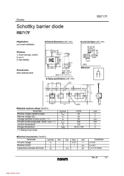
Diodes
Schottky barrier diode
RB717F
zApplications Low current rectification z External dimensions (Unit : mm) z Land size figure (Unit : mm)
㪈㪅㪊
r
㪬㪤㪛㪊
r
zStructure
zConstruction Silicon epitaxial planar
㩷
㪩㪦㪟㪤㩷㪑㩷㪬㪤㪛㪊 㪡㪜㪛㪜㪚㩷㪑㩷㪪㪦㪫㪄㪊㪉㪊 㪡㪜㪠㪫㪘㩷㪑㩷㪪㪚㪄㪎㪇 㪻㫆㫋㩷㩿㫐㪼㪸㫉㩷㫎㪼㪼㫂㩷㪽㪸㪺㫋㫆㫉㫐㪀
z Taping specifications (Unit : mm)
㪈㪉㪌
㪇
㪉㪌
㪌㪇
㪎㪌
㪈㪇㪇
㪈㪉㪌
㪚㪘㪪㪜㩷㪫㪜㪤㪧㪘㪩㪘㪫㪬㪩㪜㪑㪫㪺㩿㷄㪀 㪛㪼㫉㪸㫋㫀㫅㪾㩷㪚㫌㫉㫍㪼䍼㩿㪠㫆㪄㪫㪺㪀
Rev.B
3/3
/
Appendix
Notes
No technical content pages of this document may be reproduced in any form or transmitted by any means without prior permission of ROHM CO.,LTD. The contents described herein are subject to change without notice. The specifications for the product described in this document are for reference only. Upon actual use, therefore, please request that specifications to be separately delivered. Application circuit diagrams and circuit constants contained herein are shown as examples of standard use and operation. Please pay careful attention to the peripheral conditions when designing circuits and deciding upon circuit constants in the set. Any data, including, but not limited to application circuit diagrams information, described herein are intended only as illustrations of such devices and not as the specifications for such devices. ROHM CO.,LTD. disclaims any warranty that any use of such devices shall be free from infringement of any third party's intellectual property rights or other proprietary rights, and further, assumes no liability of whatsoever nature in the event of any such infringement, or arising from or connected with or related to the use of such devices. Upon the sale of any such devices, other than for buyer's right to use such devices itself, resell or otherwise dispose of the same, no express or implied right or license to practice or commercially exploit any intellectual property rights or other proprietary rights owned or controlled by ROHM CO., LTD. is granted to any such buyer. Products listed in this document are no antiradiation design.
FMMT717中文资料
-55°C 25°C 100°C
VCE(SAT) vs IC
1.2 1.0 450 0.8 0.6 225 0.4 0.2 0.0 1mA
-55°C 25°C 100°C
V+-=5V
I+/I*=5
VBE( sat) VBE(on) hFE 300 300 175 40
-0.94 -0.78 470 450 275 60 10
475 450 375 250 30
Transition Frequency
fT
150
200
150 20
200 13 50 760 20
Output Capacitance Cob o Turn-On Time Turn-Off Time t(on) t(off)
10mA
100mA
1A
10A
Collector Current
Collector Current
hFE vs IC
VBE(SAT) vs IC
10 SINGLE PULSE TEST Tamb = 25 deg C
1.0 0.8 0.6 0.4 0.2
V+-=5V
-55°C
25°C
1.0
D.C. 1s 100ms 10ms 1ms 100µs
FMMT723
TYP. -200 -160 -8.8 MAX.
MAX. MIN.
UNIT CONDITIONS. V V V nA nA nA nA nA mV mV mV mV mV mV V V IC =-100µA IC =-10mA* IE=-100µA VC B=-60V VC B=-80V VEB=-4V VC ES=-60V VC ES=-80V IC =-0.1A, IB=-10mA* IC =-0.5A, IB=-20mA* IC =-0.5A, IB=-50mA* IC =-1A, IB=-100mA* IC =-1A, IB=-150mA* IC =-1.5A, IB=-200mA* IC =-1A, IB=-150mA* IC =-1.5A, IB=-200mA* IC =-1A, VC E=-10V* IC =-1.5A, VC E=-5V* IC =-10mA, VC E=-5V* IC =-10mA, VC E=-10V* IC =-0.1A, VC E=-5V* IC =-0.1A, VC E=-10V* IC =-0.5A, VC E=-10V* IC =-1A, VC E=-5V* IC =-1A, VC E=-10V* IC =-1.5A, VC E=-5V* IC =-1.5A, VC E=-10V* IC =-3A, VC E=-5V* MHz IC =-50mA, VC E=-10V f=100MHz VC B=-10V, f=1MHz VC C =-50V, IC =-0.5A IB1 =IB2 =-50mA
9906;中文规格书,Datasheet资料
Nominal data
Type Phase Nominal voltage Frequency Speed Power input Min. ambient temperature Max. ambient temperature Air flow Sound power level Sound pressure level VAC Hz min-1 W °C °C m3/h B dB(A) 9906 1~ 115 60 2850 12.0 -40 70 135 5.4 42
/
9906
AC axial compact fan
Technical features
General description AC voltage fan with internal rotor shaded-pole motor. Protected from overload by impedance protection. Fan housing made of metal, impeller made of mineral-reinforced PA plastic. Air exhaust over bars. Direction of rotation counter-clockwise seen on rotor. Electrical connection to 2 flat plugs 2.8 x 0.5 mm. Fan housing with grounding lug for M4 tapping screw. Mass 320 g. Please note our new ACmaxx series. With identical fastening dimensions and voltages, this series achieves higher energy efficiency. 0.325 kg 119 x 119 x 25 mm Mineral-reinforced PA plastic Metal Air exhaust over bars Left, looking at rotor Ball bearings 52500 h 25000 h 2 flat plugs 2.8 x 0.5 mm Protected from overload using impedance protection VDE, CSA, UL, CE
ADZS-BF609-EZLITE;ADZS-BF609-EZBRD;中文规格书,Datasheet资料
ADSP-BF609 EZ-KIT Lite®Evaluation System ManualRevision 1.0, March 2012Part Number82-000269-01 Analog Devices, Inc.One T echnology WayaNorwood, Mass. 02062-9106Copyright Information© 2012 Analog Devices, Inc., ALL RIGHTS RESERVED. This docu-ment may not be reproduced in any form without prior, express writtenconsent from Analog Devices, Inc.Printed in the USA.DisclaimerAnalog Devices, Inc. reserves the right to change this product withoutprior notice. Information furnished by Analog Devices is believed to beaccurate and reliable. However, no responsibility is assumed by AnalogDevices for its use; nor for any infringement of patents or other rights ofthird parties which may result from its use. No license is granted by impli-cation or otherwise under the patent rights of Analog Devices, Inc. Trademark and Service Mark NoticeThe Analog Devices logo, Blackfin, CrossCore, EZ-Board, EZ-Extender, and EZ-KIT Lite are registered trademarks of Analog Devices, Inc.All other brand and product names are trademarks or service marks oftheir respective owners.Regulatory ComplianceThe ADSP-BF609 EZ-KIT Lite is designed to be used solely in a labora-tory environment. The board is not intended for use as a consumer end product or as a portion of a consumer end product. The board is an open system design which does not include a shielded enclosure and therefore may cause interference to other electrical devices in close proximity. This board should not be used in or near any medical equipment or RF devices.The ADSP-BF609 EZ-KIT Lite is currently being processed for certifica-tion that it complies with the essential requirements of the EuropeanEMC directive 2004/108/EC and therefore carries the “CE” mark.The EZ-KIT Lite evaluation system contains ESD (electrostatic discharge)sensitive devices. Electrostatic charges readily accumulate on the humanbody and equipment and can discharge without detection. Permanent dam-age may occur on devices subjected to high-energy discharges. Proper ESDprecautions are recommended to avoid performance degradation or loss offunctionality. Store unused EZ-KIT Lite boards in the protective shippingpackage.PREFACEProduct Overview (xii)Purpose of This Manual (xv)Intended Audience (xv)Manual Contents (xvi)What’s New in This Manual (xvi)Technical or Customer Support (xvii)Supported Processors (xvii)Product Information (xviii)Analog Devices Web Site (xviii)EngineerZone (xviii)Related Documents (xix)Notation Conventions (xx)USING ADSP-BF609 EZ-KIT LITEPackage Contents .......................................................................... 1-2 ADSP-BF609 EZ-Board ................................................................ 1-3 Default Configuration ................................................................... 1-3 Supported Operating Systems ....................................................... 1-5ADSP-BF609 EZ-KIT Lite Evaluation System Manual vSystem Requirements .................................................................... 1-5 EZ-KIT Lite Installation ............................................................... 1-6 EZ-KIT Lite Session Startup ......................................................... 1-7 Evaluation License Restrictions ................................................... 1-10 Memory Map ............................................................................. 1-10 DDR2 SDRAM .......................................................................... 1-12 SPI Interface .............................................................................. 1-13 SMC Interface ............................................................................ 1-13 Ethernet Interface ....................................................................... 1-13 USB OTG HS Interface .............................................................. 1-14 CAN Interface ............................................................................ 1-14 UART Interface .......................................................................... 1-15 SD Interface ............................................................................... 1-16 Rotary Encoder Interface ............................................................ 1-16 Temperature Sensor Interface ...................................................... 1-17 Link Ports Interface .................................................................... 1-17 General-Purpose I/O (GPIO) ...................................................... 1-18 JTAG Interface ........................................................................... 1-18 Power-On-Self Test ..................................................................... 1-20 Expansion Interface III ............................................................... 1-20 Power Architecture ..................................................................... 1-21 Power Measurements .................................................................. 1-21 Example Programs ...................................................................... 1-22 Reference Design Information ..................................................... 1-22vi ADSP-BF609 EZ-KIT Lite Evaluation System ManualADSP-BF609 EZ-KIT LITE HARDWARE REFERENCE System Architecture ...................................................................... 2-2 Software-Controlled Switches (SoftConfig) .................................... 2-3 Overview of SoftConfig ........................................................... 2-3SoftConfig on the ADSP-BF609 EZ-KIT LITE ...................... 2-7Programming SoftConfig Switches ........................................... 2-8 Push Buttons and Switches .......................................................... 2-17 JTAG Interface Switches (SW1, SW3–5) ................................ 2-18Boot Mode Select Switch (SW2) ............................................ 2-19IRQ/Flag Enable Switches (SW6–7) ....................................... 2-20Reset Switch (SW8) ............................................................... 2-20Rotary Encoder With Momentary Switch (SW9) .................... 2-20Wake Push Switch (SW10) .................................................... 2-21 Power Jumpers ............................................................................ 2-21 LEDs .......................................................................................... 2-22 GPIO LEDs (LED1–4) ......................................................... 2-23Thermal Limit LED (LED5) ................................................. 2-23Power LED (LED6) ............................................................... 2-23Reset LED (LED7) ................................................................ 2-24SPD LED (LED6) ................................................................. 2-24 Connectors ................................................................................. 2-24 DCE UART Connector (J2) .................................................. 2-25Link Port /JTAG Connectors (J3 and P8) ............................... 2-25JTAG Connector (P1) ........................................................... 2-25 ADSP-BF609 EZ-KIT Lite Evaluation System Manual viiJTAG Connector (ZP1) ......................................................... 2-26Expansion Interface III Connectors (P1A–C, P2A, P3A) ........ 2-26USB Connector (P7) ............................................................. 2-26Power Connector (P18) ......................................................... 2-26CAN Connector (J4) ............................................................ 2-27SD Connector (J5) ................................................................ 2-27Ethernet Connector (J1) ....................................................... 2-27Ethernet Connectors (P16-17) ............................................... 2-27 ADSP-BF609 EZ-KIT LITE BILL OF MATERIALSADSP-BF609 EZ-KIT LITE SCHEMATICTitle Page ..................................................................................... B-1 Processor DDR2 Interface ............................................................ B-2 Processor Signals ........................................................................... B-3 Processor Power and Ground ......................................................... B-4 Temp Sensor, Boot Switch, DSP CLK, USB Conn ......................... B-5 Memory ....................................................................................... B-6 UART0 ........................................................................................ B-7 CAN and Rotary Encoder ............................................................. B-8 Ethernet ....................................................................................... B-9JTAG, Link Port 0 and 1 ........................................................... B-10 Push Buttons, Reset, LEDs ......................................................... B-11 SoftConfig Switches, IO Extender ICs ......................................... B-12 Expansion Interface, Page 1 ........................................................ B-13viii ADSP-BF609 EZ-KIT Lite Evaluation System ManualExpansion Interface, Page 2 ........................................................ B-14 Expansion Interface, Page 3 ........................................................ B-15 Power ........................................................................................ B-16 INDEXADSP-BF609 EZ-KIT Lite Evaluation System Manual ixx ADSP-BF609 EZ-KIT Lite Evaluation System Manual分销商库存信息: ANALOG-DEVICESADZS-BF609-EZLITE ADZS-BF609-EZBRD。
TC826CBU;TC826CBU713;中文规格书,Datasheet资料

© 2005 Microchip Technology Inc.DS21477C-page 1TC826Features•Bipolar A/D Conversion • 2.5% Resolution•Direct LCD Display Drive•‘Thermometer’ BAR or DOT Display •40 Data Segments Plus Zero•Over Range Plus Polarity Indication•Precision On-Chip Reference: 35ppm/°C •Differential Analog Input •Low Input Leakage: 10pA•Display Flashes on Over Range •Display HOLD Mode•Auto-Zero Cycle Eliminates Zero Adjust Potentiometer•9V Battery Operation•Low Power Consumption: 1.1mW •20mV to 2.0V Full Scale Operation•Non-Multiplexed LCD Drive for Maximum Viewing AngleDevice Selection TableGeneral DescriptionIn many applications, a graphical display is preferred over a digital display. Knowing a process or system operates, for example, within design limits is more valu-able than a direct system variable read out. A bar or moving dot display supplies information precisely with-out requiring further interpretation by the viewer.The TC826 is a complete analog-to-digital converter with direct liquid crystal (LCD) display drive. The 40LCD data segments plus zero driver give a 2.5% reso-lution bar display. Full scale differential input voltage range extends from 20mV to 2V. The TC826 sensitivity is 500μV. A low drift 35ppm/°C internal reference, LCD backplane oscillator and driver, input polarity LCD driver, and over range LCD driver make designs simple and low cost. The CMOS design required only 125µA from a 9V battery. In +5V systems, a TC7660 DC to DC converter can supply the -5V supply. The differential analog input leakage is a low 10pA.Two display formats are possible. The BAR mode dis-play is like a ‘thermometer’ scale. The LCD segment driver that equals the input, plus all below it are on. The DOT mode activates only the segment equal to the input. In either mode, the polarity signal is active for negative input signals. An over range input signal causes the display to flash and activates the over range annunciator. A HOLD mode can be selected that freezes the display and prevents updating.The dual slope integrating conversion method with auto-zero phase maximizes noise immunity and elimi-nates zero scale adjustment potentiometers. Zero scale drift is a low 5μV/°C. Conversion rate is typically 5 per second and is adjustable by a single external resistor.A compact, 0.5" square, flat package minimizes PC board area. The high pin count LSI package makes multiplexed LCD displays unnecessary. Low cost,direct drive LCD displays offer the widest viewing angle and are readily available. A standard display is avail-able now for TC826 prototyping work.Part Number Package Temperature RangeTC826CBU64-Pin PQFP0°C to +70°CAnalog-to-Digital Converter with Bar Graph Display OutputObsolete DeviceTC826DS21477C-page 2© 2005 Microchip Technology Inc.© 2005 Microchip Technology Inc.DS21477C-page 3TC8261.0ELECTRICALCHARACTERISTICSAbsolute Maximum Ratings*Supply Voltage (V+ to V-).......................................15V Analog Input Voltage (Either Input) (Note 1)...V+ to V-Power Dissipation (T A ≤ 70°C)64-Pin Plastic Flat Package...............................1.14W Operating Temperature Range:Commercial Package (C)........................0°C to +70°C Storage Temperature Range..............-65°C to +150°C*Stresses above those listed under "Absolute Maximum Ratings" may cause permanent damage to the device. These are stress ratings only and functional operation of the device at these or any other conditions above those indicated in the operation sections of the specifications is not implied.Exposure to Absolute Maximum Rating conditions for extended periods may affect device reliability.TC826 ELECTRICAL SPECIFICATIONSNote 1:Input voltages may exceed the supply voltages when the input current is limited to 100μA.2:Static sensitive device. Unused devices should be stored in conductive material to protect devices from static dischargeand static fields.3:Backplane drive is in phase with segment drive for ‘off’ segment and 180°C out of phase for ‘on’ segment. Frequency is10 times conversion rate.4:Logic input pins 58, 59, and 60 should be connected through 1M Ω series resistors to V SS for logic 0.Electrical Characteristics: V S = 9V; R OSC = 430k Ω; T A = 25°C; Full Scale = 20mV, unless otherwise stated.SymbolParameterMin Typ Max Unit Test ConditionsZero Input -0±0 +0Display V IN = 0.0V Zero Reading Drift—0.2 1μV/°C V IN = 0.0V0°C ≤ T A ≤ +70°CNL Linearity Error -10.5 +1Count Max Deviation from Best Straight Line R/O Rollover Error -10 +1Count -V IN = +V IN EN Noise—60 —μV P-P V IN = 0V ILK Input Leakage Current —10 20pA V IN = 0V CMRRCommon Mode Rejection Ratio —50 —μV/V VCM = ±1V V IN = 0VScale Factor Temperature Coefficient—1—ppm/°C0 ≤ T A ≤ 7 +0°CExternal Ref. Temperature Coefficient = 0ppm/°C V CTC Analog Common Temperature Coefficient—35 100ppm/°C 250k Ω between Common and V+, 0°C ≤ T A ≤ +70°CV COM Analog Common Voltage 2.7 2.9 3.35V 250k Ω between Common and V DDVSD LCD Segment Drive Voltage 45 6V P-P VBD LCD Backplane Drive Voltage 45 6V P-P I DDPower Supply Current—125175μATC826DS21477C-page 4© 2005 Microchip Technology Inc.2.0PIN DESCRIPTIONThe descriptions of the pins are listed in Table 2-1.TABLE 2-1:PIN FUNCTION TABLEPin Number (64-Pin PQFP)Symbol Description1NC Positive analog signal input.2ANALOG COMMONEstablishes the internal analog ground point. Analog common is set to 2.9V below the positive supply COMMON by an internal zener reference circuit. The voltage difference between V DD and analog common can be used to supply the TC826 voltage reference input at REF IN (Pin 5).3+IN Positive analog signal input.4-IN Negative analog signal input.5REF IN Reference voltage positive input. Measured relative to analog common. REF IN ≈ Full Scale/2.6C REF +Reference capacitor connection.7C REF -Reference capacitor connection.8V DD Positive supply terminal.9V BUF Buffer output. Integration resistor connection.10C AZ Negative comparator input. Auto-zero capacitor connection.11V INT Integrator output. Integration capacitor connection.12V SS Negative supply terminal.13OSC1Oscillator resistor (R OSC ) connection.14OSC2Oscillator resistor (R OSC ) connection.15BP LCD Backplane driver. 16BAR 0LCD Segment driver: Bar 0.17NC No connection.18BAR 1LCD Segment driver: Bar 1.19BAR 2LCD Segment driver: Bar 2.20BAR 3LCD Segment driver: Bar 3.21BAR 4LCD Segment driver: Bar 4.22BAR 5LCD Segment driver: Bar 5.23BAR 6LCD Segment driver: Bar 6.24BAR 7LCD Segment driver: Bar 7.25BAR 8LCD Segment driver: Bar 8.26BAR 9LCD Segment driver: Bar 9.27BAR 10LCD Segment driver: Bar 10.28BAR 11LCD Segment driver: Bar 11.29BAR 12LCD Segment driver: Bar 12.30BAR 13LCD Segment driver: Bar 13.31BAR 14LCD Segment driver: Bar 14.32BAR 15LCD Segment driver: Bar 15.33BAR 16LCD Segment driver: Bar 16.34BAR 17LCD Segment driver: Bar 17.35BAR 18LCD Segment driver: Bar 18.36BAR 19LCD Segment driver: Bar 19.37BAR 20LCD Segment driver: Bar 20.38BAR 21LCD Segment driver: Bar 21.39BAR 22LCD Segment driver: Bar 22.40BAR 23LCD Segment driver: Bar 23.© 2005 Microchip Technology Inc.DS21477C-page 5TC82641BAR 24LCD Segment driver: Bar 24.42BAR 25LCD Segment driver: Bar 25.43BAR 26LCD Segment driver: Bar 26.44BAR 27LCD Segment driver: Bar 27.45BAR 28LCD Segment driver: Bar 28.46BAR 29LCD Segment driver: Bar 29.47BAR 30LCD Segment driver: Bar 30.48NC No connection.49BAR 31LCD Segment driver: Bar 31.50BAR 32LCD Segment driver: Bar 32.51BAR 33LCD Segment driver: Bar 33.52BAR 34LCD Segment driver: Bar 34.53BAR 35LCD Segment driver: Bar 35.54BAR 36LCD Segment driver: Bar 36.55BAR 37LCD Segment driver: Bar 37.56BAR 38LCD Segment driver: Bar 38.57BAR 39LCD Segment driver: Bar 39.58BAR 40LCD Segment driver: Bar 40.59OR LCD segment driver that indicated input out-of-range condition.60POL-LCD segment driver that indicates input signal is negative.61BAR/DOT Input logic signal that selects BAR or DOT display format. Normally in BAR mode. Connect to V SS through 1M Ω resistor for DOT format.62HOLD Input logic signal that prevents display from changing. Pulled high internally to inactive state. Connect to V SS through 1M Ω series resistor for HOLD mode operation.63TESTInput logic signal. Sets TC826 to BAR Display mode. BAR 0 to 40, plus OR flash on and off. The POL- LCD driver is on. Pulled high internally to inactive state. Connect to V SS with 1M Ω series resistor to activate.64NCNo connection.TABLE 2-1:PIN FUNCTION TABLE (CONTINUED)Pin Number (64-Pin PQFP)Symbol DescriptionTC826DS21477C-page 6© 2005 Microchip Technology Inc.3.0DETAILED DESCRIPTION3.1Dual Slope Conversion PrinciplesThe TC826 is a dual slope, integrating analog-to-digital converter. The conventional dual slope converter mea-surement cycle has two distinct phases:•Input Signal Integration•Reference Voltage Integration (De-integration)The input signal being converted is integrated for a fixed time period (T SI ). Time is measured by counting clock pulses. An opposite polarity constant reference voltage is then integrated until the integrator output voltage returns to zero. The reference integration time is directly proportional to the input signal (T RI )(Figure 3-1).In a simple dual slope converter, a complete conver-sion requires the integrator output to ‘ramp-up’ and ‘ramp-down’.A simple mathematical equation relates the input signal reference voltage and integration time:EQUATION 3-1:1RCt INT 0V IN (t)dt =V R TRI RC∫Where:V R = Reference VoltageV SI = Signal Integration Time (Fixed)T RI = Reference Voltage Integration Time(Variable)TC826For a constant V IN:EQUATION 3-2:The dual slope converter accuracy is unrelated to the integrating resistor and capacitor values, as long as they are stable during a measurement cycle. An inher-ent benefit is noise immunity. Noise spikes are inte-grated or averaged to zero during the integration periods. Integrating ADCs are immune to the large con-version errors that plague successive approximation converters in high noise environments. Interfering sig-nals with frequency components at multiples of the averaging period will be attenuated (Figure3-2).The TC826 converter improves the conventional dual slope conversion technique by incorporating an auto-zero phase. This phase eliminates zero scale offset errors and drift. A potentiometer is not required to obtain a zero output for zero input.FIGURE 3-2:NORMAL MODEREJECTION OF DUALV IN = V R T RI T SI© 2005 Microchip Technology Inc.DS21477C-page 7TC826DS21477C-page 8© 2005 Microchip Technology Inc.4.0THEORY OF OPERATION4.1Analog SectionIn addition to the basic signal integrate and de-integrate cycles discussed above, the TC826 incorpo-rates an auto-zero cycle.This cycle removes buffer amplifier, integrator, and comparator offset voltage error terms from the conversion. A true digital zero reading results without external adjusting potentiome-ters. A complete conversion consists of three cycles:an auto-zero, signal integrate and reference cycle (Figure 4-1 and Figure 4-2).4.1.1AUTO-ZERO CYCLE During the auto-zero cycle, the differential input signal is disconnected from the circuit by opening internal analog gates. The internal nodes are shorted to analog common (internal analog ground) to establish a zero input condition. Additional analog gates close a feed-back loop around the offset voltage error compensation.The voltage level established on C AZ compensates for device offset voltages.The auto-zero cycle length is 19 counts minimum.Unused time in the de-integrate cycle is added to the auto-zero cycle.4.1.2SIGNAL INTEGRATION CYCLEThe auto-zero loop is opened and the internal differen-tial inputs connect to +IN and -IN. The differential input signal is integrated for a fixed time period. The TC826signal integration period is 20 clock periods or counts.The externally set clock frequency is divided by 32before clocking the internal counters. The integration time period is:EQUATION 4-1:Where:F OSC = External Clock FrequencyT SI =32F OSCx 20© 2005 Microchip Technology Inc.DS21477C-page 9TC826The differential input voltage must be within the device Common mode range when the converter and mea-sured system share the same power supply common (ground). If the converter and measured system do not share the same power supply common, -IN should be tied to analog common. This is the usual connection for battery operated systems. Polarity is determined at the end of signal integrate signal phase. The sign bit is a true polarity indication, in that signals less than 1LSB are correctly determined. This allows precision null detection limited only by device noise and system noise.4.1.3REFERENCE INTEGRATE CYCLEThe final phase is reference integrate or de-integrate.-IN is internally connected to analog common and +IN is connected with the correct polarity to cause the inte-grator output to return to zero. The time required for the output to return to zero is proportional to the input sig-nal and is between 0 and 40 counts. The digital reading displayed is:EQUATION 4-2:20 =V IN V REFTC826DS21477C-page 10© 2005 Microchip Technology Inc.4.2System TimingThe oscillator frequency is divided by 32 prior to clock-ing the internal counters. The three-phase measure-ment cycle takes a total of 80 clock pulses. The 80count cycle is independent of input signal magnitude.Each phase of the measurement cycle has the follow-ing length:•Auto-Zero Phase: 19 to 59 CountsFor signals less than full scale, the auto-zero isassigned the unused reference integrate time period.•Signal Integrate: 20 CountsThis time period is fixed. The integration period is:EQUATION 4-3:•Reference Integrate: 0 to 41 Counts4.3Reference Voltage SelectionA full scale reading requires the input signal be twice the reference voltage. The reference potential is mea-sured between REF IN (Pin 5) and ANALOG COMMON (Pin 2).TABLE 4-1:The internal voltage reference potential available at analog common will normally be used to supply the converter’s reference. This potential is stable when-ever the supply potential is greater than approximately 7V. In applications where an externally generated refer-ence voltage is desired, refer to Figure 4-3.The reference voltage is adjusted with a near full scale input signal. Adjust for proper LCD display read out.4.4Components Value Selection4.4.1INTEGRATING RESISTOR (R INT )The desired full scale input voltage and output current capability of the input buffer and integrator amplifier set the integration resistor value. The internal class A out-put stage amplifiers will supply a 1μA drive current with minimal linearity error. R INT is easily calculated for a 1μA full scale current:EQUATION 4-4:4.4.2INTEGRATING CAPACITOR (C INT )The integrating capacitor should be selected to maxi-mize integrator output swing. The integrator output will swing to within 0.4V of V S + or V S - without saturating.The integrating capacitor is easily calculated:EQUATION 4-5:The integrating capacitor should be selected for low dielectric absorption to prevent rollover errors. Polypro-pylene capacitors are suggested.4.4.3AUTO-ZERO CAPACITOR (C AZ )C AZ should be 2-3 times larger than the integration capacitor. A polypropylene capacitor is suggested. Typ-ical values from 0.14μF to 0.068μF are satisfactory.4.4.4REFERENCE CAPACITOR (C REF )A 1μF capacitor is suggested. Low leakage capacitors,such as polypropylene, are recommended.Several capacitor/resistor combinations for common full scale input conditions are given in Table 4-2.Required Full Scale VoltageV REF 20mV 10mV 2V1VT SI = 20⎛⎝⎞⎠32F OSC Where F OSC is the externally set clock frequency.Where V FS = Full Scale Analog InputR INT =Full Scale Voltage(V)1 x 10 – 6V FS 1 x 10 – 6=Where: V INT = Integrator SwingF OSC = Oscillator FrequencyC INT =V FS R INT ⎛⎝⎞⎠640F OSC x V INT分销商库存信息:MICROCHIPTC826CBU TC826CBU713。
ZNI1000TA;ZNI1000TC;中文规格书,Datasheet资料
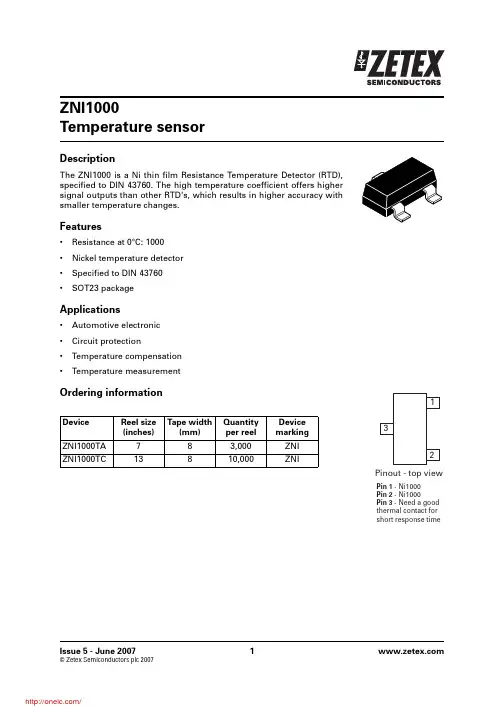
ZNI1000Temperature sensorDescriptionThe ZNI1000 is a Ni thin film Resistance Temperature Detector (RTD), specified to DIN 43760. The high temperature coefficient offers higher signal outputs than other RTD's, which results in higher accuracy with smaller temperature changes.Features•Resistance at 0°C: 1000•Nickel temperature detector•Specified to DIN 43760•SOT23 packageApplications•Automotive electronic•Circuit protection•Temperature compensation•Temperature measurementOrdering informationDevice Reel size(inches)Tape width(mm)Quantityper reelDevicemarkingZNI1000TA783,000ZNI ZNI1000TC13810,000ZNIAbsolute maximum ratingsNOTES:(a)Limited by operating temperature [ I CC Յ(20mW/R)½ , R=func(T A )=718 to 1986⍀].Recommended operating conditionsNOTES:(b)limited by self heating effects (recommended current range 0,1 to 1,5mA)[ typ. case → temperature error ⌬T= (R и1,2mA и1,2mA)/1,7mW/K Յ 1,7K ][ worst case → temperature error ⌬T= (1,986k ⍀и3,0mA и3,0mA)/1,4mW/K = 13,8K ].Electrical characteristicsNOTES:(c)Measured under pulse conditions.(d)See ZNi1000 Tolerance class figure.Parameter S ymbol Limit Unit Continuous current (a)I CC 5 mA Total power dissipation P TOT 20mW Operating temperature range T A -55to +150 °C Storage temperature rangeT stg -55to +150 °C Symbol Parameter Min.Typ.Max.Unit I MDCSteady state measurement current (b)0,11,23,0mASymbol ParameterConditions Min.Typ.Max.Unit R0Resistance 0°C T=0°C, I M <1mA -1000-⍀R25Resistance 25°C T=25°C, I M = 3mA (c)110011411200⍀R100Resistance 100°C T=100°C, I M <1mA-1618-⍀Tolerance class B (d)-55 to 0°C -±(0.4+0.028 x ¦T¦)-°C Tolerance class B (d)0 to 150°C -±(0.4+0.007 x ¦T¦)-°C ⌬RLong Term stability:1000h at 150°C0.1%Characteristics according to DIN43760Resistance at a given temperature R(T) = R0 x (1 + A x T + B x T 2 + C x T 4+ D x T 6)Formula for temperature at a given resistancecoefficients:A = -412.6B = 140.41C = 0.00764D = -6.25 x 10⁻¹⁷E = -1.25 x 10⁻²⁴Self heatingFor accurate temperature measurement it's recommended to choose a small current in order to avoid self heating of the resistor. The temperature failure caused by the measurement current can be calculated with:⌬T = P/EKwhere P = I² * R is the heat power caused by the measurement current and EK is the self heating coefficient.The self heating coefficient for the Ni1000-SOT is: EK = (1.7 ± 0.3) mW/K (Air: 23°C; no air flow).R0Resistance at 0°C B 6.650 x 10⁻⁶T Temperature in °C C 2.805 x 10⁻¹¹ A5.485 x 10-3D-2.000 x 10⁻¹⁷T R ()A B 1C R ×+×D R 5×E R7×+++=Package outline - SOT23Note: Controlling dimensions are in millimeters. Approximate dimensions are provided in incheslimeters Inches limeters Inches Min.Max.Min.Max.Min.Max.Min.Max.A - 1.12-0.044e1 1.90 NOM0.075 NOMA10.010.100.00040.004E 2.10 2.640.0830.104b 0.300.500.0120.020E1 1.20 1.400.0470.055c 0.0850.200.0030.008L 0.250.600.00980.0236D 2.803.040.1100.120L10.450.620.0180.024e0.95 NOM 0.037 NOM-----Zetex sales offices EuropeZetex GmbHKustermann-park Balanstraße 59D-81541 München GermanyTelefon: (49) 89 45 49 49 0Fax: (49) 89 45 49 49 49europe.sales@AmericasZetex Inc700 Veterans Memorial Highway Hauppauge, NY 11788USATelephone: (1) 631 360 2222Fax: (1) 631 360 8222usa.sales@Asia PacificZetex (Asia Ltd)3701-04 Metroplaza Tower 1Hing Fong Road, Kwai Fong Hong KongTelephone: (852) 26100 611Fax: (852) 24250 494asia.sales@Corporate HeadquartersZetex Semiconductors plcZetex Technology Park, Chadderton Oldham, OL9 9LL United KingdomTelephone: (44) 161 622 4444Fax: (44) 161 622 4446hq@© 2007 Published by Zetex Semiconductors plcDefinitionsProduct changeZetex Semiconductors reserves the right to alter, without notice, specifications, design, price or conditions of supply of any product or service. Customers are solely responsible for obtaining the latest relevant information before placing orders.Applications disclaimerThe circuits in this design/application note are offered as design ideas. It is the responsibility of the user to ensure that the circuit is fit for the user’s application and meets with the user’s requirements. No representation or warranty is given and no liability whatsoever is assumed by Zetex with respect to the accuracy or use of such information, or infringement of patents or other intellectual property rights arising from such use or otherwise. Zetex does not assume any legal responsibility or will not be held legally liable (whether in contract,tort (including negligence), breach of statutory duty, restriction or otherwise) for any damages, loss of profit, business, contract,opportunity or consequential loss in the use of these circuit applications, under any circumstances.Life supportZetex products are specifically not authorized for use as critical components in life support devices or systems without the express written approval of the Chief Executive Officer of Zetex Semiconductors plc. As used herein:A. Life support devices or systems are devices or systems which:1.are intended to implant into the body or2.support or sustain life and whose failure to perform when properly used in accordance with instructions for use provided in the labeling can be reasonably expected to result in significant injury to the user.B. A critical component is any component in a life support device or system whose failure to perform can be reasonably expected tocause the failure of the life support device or to affect its safety or effectiveness.ReproductionThe product specifications contained in this publication are issued to provide outline information only which (unless agreed by the company in writing) may not be used, applied or reproduced for any purpose or form part of any order or contract or be regarded as a representation relating to the products or services concerned. Terms and ConditionsAll products are sold subjects to Zetex’ terms and conditions of sale, and this disclaimer (save in the event of a conflict between the two when the terms of the contract shall prevail) according to region, supplied at the time of order acknowledgement.For the latest information on technology, delivery terms and conditions and prices, please contact your nearest Zetex sales office.Quality of productZetex is an ISO 9001 and TS16949 certified semiconductor manufacturer.To ensure quality of service and products we strongly advise the purchase of parts directly from Zetex Semiconductors or one of our regionally authorized distributors. For a complete listing of authorized distributors please visit: /salesnetworkZetex Semiconductors does not warrant or accept any liability whatsoever in respect of any parts purchased through unauthorized sales channels.ESD (Electrostatic discharge)Semiconductor devices are susceptible to damage by ESD. Suitable precautions should be taken when handling and transporting devices.The possible damage to devices depends on the circumstances of the handling and transporting, and the nature of the device. The extent of damage can vary from immediate functional or parametric malfunction to degradation of function or performance in use over time.Devices suspected of being affected should be replaced.Green complianceZetex Semiconductors is committed to environmental excellence in all aspects of its operations which includes meeting or exceeding reg-ulatory requirements with respect to the use of hazardous substances. Numerous successful programs have been implemented to reduce the use of hazardous substances and/or emissions.All Zetex components are compliant with the RoHS directive, and through this it is supporting its customers in their compliance with WEEE and ELV directives.Product status key:“Preview”Future device intended for production at some point. Samples may be available “Active”Product status recommended for new designs “Last time buy (LTB)”Device will be discontinued and last time buy period and delivery is in effect “Not recommended for new designs”Device is still in production to support existing designs and production “Obsolete”Production has been discontinued Datasheet status key:“Draft version”This term denotes a very early datasheet version and contains highly provisional information, whichmay change in any manner without notice.“Provisional version”This term denotes a pre-release datasheet. It provides a clear indication of anticipated performance.However, changes to the test conditions and specifications may occur, at any time and without notice.“Issue”This term denotes an issued datasheet containing finalized specifications. However, changes tospecifications may occur, at any time and without notice.分销商库存信息:DIODESZNI1000TA ZNI1000TC。
UDZSTE-1711B;中文规格书,Datasheet资料
Land size figure (Unit : mm)
0.9MIN. 0.8MIN.
1.7±0.1
2.5±0.2
UMD2
0.7±0.2 0.1
Structure
0.3±0.05
Construction Silicon epitaxial planar
20 19 CAPACITANCE BETWEENTERMINALS:Ct(pF) 18 17 16 15 14 13 12 11 10 AVE:16.76pF Ta=25℃ f=1MHz VR=0V n=10pcs
11.8 ZENER VOLTAGE:Vz(V)
11.7
11.6
11.5 AVE:10.943V 11.4
0.1 0.001
0.01
0.1
1
10
100
TIME:t(ms) PRSM-TIME CHARACTERISTICS 1000 Rth(j-a)
100
Rth(j-c)
10
Mounted on epoxy board IM=10mA IF=100mA
1
1ms time
300us
0.1 0.001
0.01
Zener diode
UDZS11B
Applications Constant voltage control Features 1) Compact, 2-pin mini-mold type for high-density mounting. (UMD2) 2) High reliability. 3) Can be mounted automatically, using chip mounter. Dimensions (Unit : mm)
电子元器件ZUMT717中文资料_数据手册_IC数据表
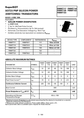
Super323™ SOT323 PNP SILICON POWER (SWITCHING) TRANSISTORISSUE 1 - SEPTEMBER 1998FEATURES*500mW POWER DISSIPATION*I C CONT 1.5A*3A Peak Pulse Current*Excellent H FE Characteristics Up To 3A (pulsed)*Extremely Low Saturation Voltage*Extremely Low Equivalent On Resistance; R CE(sat)APPLICATIONS *Negative boost functions in DC-DC converters *Supply line switching in mobile phones and pagers *Motor drivers in camcorders and mini disk players†Recommended P tot calculated using FR4 measuring 10 x 8 x 0.6mm (still air).‡Maximum power dissipation is calculated assuming that the device is mounted on FR4size 25x25x0.6mm and using comparable measurement methods adopted by other suppliers.h tw ww n t.co mh t t p sn t.co h tt ww .i ch un t.co mh tt p s ://w w w .h t ps ://w wn t.co m.ic hu ntt pw .i ch un t.co mh tt p s://ww w.ih tt ps ://w ww .i ch un t .c o m w .i ch ut tp s:.ic hu nt .c omh tt ps ://w ww .i ch tt ps ://w w w .i c h u n t .cww .i ch i ch un t.co mh tt ps ://w ww .i ch h t t p s ://ww ww .i ch tt ps ://w ww .i ch u/w ww .i o mh tt ps ://w ww .i ch un //w ww .i ch un t.co mh tt ps ://w ww .i ch un t://w ww .i c h u n t.c o mw ww .i ch un t.s ://w w w .ich t t p sn t.co h tt p s ://w w w .un t.co m.ic h tt p s://ww w.is ://w ww .i ch un t .c o m w .i t tp s:h tt ps ://w ww .i ch tt ps ://w w w .i c h u n t .cww .i ch un h tt ps ://w ww .i ch h t t p s ://ww ww h tt ps ://w ww .i ch u/w wco mh tt ps ://w ww .i ch un //w ww .i ch un t.co mh tt ps ://w ww .i ch un t://w ww .i c h u n t.c o mw ww .i ch un t.s ://w w w .icTYPICAL CHARACTERISTICS1m1m1m100m1001m1mI C - Collector Current (A)V CE(sat)v I C0V C E (s a t )- (V )IC/IB=10IC/IB=50IC/IB=100+25°C -55°Ch F E - T y p i c a l G a i n+100°C 0I C - Collector Current (A)h FE v I CV B E (o n )- (V )I C - Collector Current (A)V BE(on)v I C+100°C +150°CV C E (s a t )- (V )+25°C 0I C - Collector Current (A)V CE(sat)v I C+100°C +150°CV B E (s a t )- (V )+25°C 0I C - Collector Current (A)V BE(sat)v I C1s 100ms I C - C o l l e c t o r C u r r e n t (A )10DC 10mV CE - Collector Emitter Voltage (V)Safe Operating Area10ms 1ms 100µs+25°C-55°C IC/IB=50VCE=2V -55°C IC/IB=50+25°C +150°C+100°C -55°C 10m100m1100.10.20.30.40.10.20.30.410m100m11020040060080010m 100m 11010m100m11010m100m1100.60.20.40.81.00.20.40.60.81.0110100m1h tt ps ://w ww .i c h u n t .c o mh t t p s n t .c o mh tt p s ://w w w .i ch u n t.c o mh tt p s ://w w w .h tt p s ://w w w .i c h un t.c o m.ic hu nt .c omh t t p s ://w w w .i c h u n t .c o mh t t p s ://ww w .ih t t p s ://w ww .i c h un t.co mw .i ch un t.co mt t p s ://w w w.i c h u n t .c o mh tt ps ://w ww .i ch tt ps ://w ww .i ch un t.cww .i ch un t.co mi c h u n t .c o mh t t ps ://w ww .i ch h t t p s ://ww ww .i ch un t.co mh tt p s ://w ww .i c h u/w ww .i ch un t.co mh t t p s ://w w w .i c h un //w ww .i ch un t.co mh t t p s ://w w w .i c h un t://w ww .i ch un t.co mw w w .i c h u n t .s ://w ww .ic。
ISL29043IROMZ-T7;中文规格书,Datasheet资料
Low Power Ambient Light and Proximity Sensor with Internal IR-LED and Digital OutputISL29043The ISL29043 is an integrated ambient and infraredlight-to-digital converter with a built-in IR LED and I 2C Interface (SMBus Compatible). This device uses two independent ADCs for concurrently measuring ambient light and proximity in parallel. The flexible interrupt scheme is designed for minimal microcontroller utilization.For ambient light sensor (ALS) data conversions, an ADCconverts photodiode current (with a light sensitivity range up to 2000 Lux) in 100ms per sample. The ADC rejects 50Hz/60Hz flicker noise caused by artificial light sources.For proximity sensor (Prox) data conversions, the built-in driver turns on an internal infrared LED and the proximity sensor ADC converts the reflected IR intensity to digital. This ADC rejects ambient IR noise (such as sunlight) and has a 540μs conversion time.The ISL29043 provides low power operation of ALS and proximity sensing with a typical 136μA normal operation current (110μA for sensors and internal circuitry, ~28μA for LED) with 220mA current pulses for a net 100μs, repeating every 800ms (or under).The ISL29043 uses both a hardware pin and software bits to indicate an interrupt event has occurred. An ALS interrupt is defined as a measurement that is outside a set window. A proximity interrupt is defined as a measurement over athreshold limit. The user may also require that both ALS/Prox interrupts occur at once, up to 16 times in a row before activating the interrupt pin.The ISL29043 is designed to operate from 2.25V to 3.63V over the -40°C to +85°C ambient temperature range. It is packaged in a clear, lead-free 10Ld ODFN package.Features•Internal LED + Sensor = Complete Solution •Works Under All Light Sources Including Sunlight •Dual ADCs Measure ALS/Prox Concurrently •<1.0μA Supply Current When Powered Down •Temperature Compensated •Pb-Free (RoHS compliant)Intelligent and Flexible Interrupts•Independent ALS/Prox Interrupt Thresholds •Adjustable Interrupt Persistency-1/4/8/16 Consecutive Triggers Required Before InterruptApplications•Display and Keypad Dimming Adjustment and Proximity Sensing for:-Mobile Devices: Smart Phone, PDA, GPS-Computing Devices: Laptop PC, Netbook, Tablet PC-Consumer Devices: LCD-TV, Digital Picture Frame, Digital Camera-Industrial and Medical Light and Proximity SensingRelated Literature•See AN1436, “Proximity Sensors”FIGURE 1.TYPICAL APPLICATION DIAGRAMFIGURE 2.PROXIMITY RESPONSE vs DISTANCE511021532042550255075100125150DISTANCE (mm)P R O X C O U N T S (8-B I T )220mA (18% GREY CARD)110mA (18% GREY CARD)110mA (WHITE COPY PAPER)220mA (WHITE COPY PAPER)ISL29043 Block DiagramPin ConfigurationISL29043(10 LD 2.1x3.5 (mm) OPTICAL CO-PACKAGE)TOP VIEWVDD REXTGNDSCL IR PHOTODIODELIGHT DATA 5463FOSCIREF IRDRARRAYALS PHOTODIODEPROCESS ALS AND IR ARRAYDUAL CHANNELADCs9INT8COMMAND REGISTERDATA REGISTERI 2CIR DRIVERINTERRUPTSDA 7ADDR02LED+1LED-10Pin DescriptionsPIN #PIN NAME DESCRIPTION0T-PAD Thermal pad. Floating - do not connect to GND or VDD 1LED+Anode of IR-LED2ADDR0I 2C address pin - pull high or low (do not float)3VDD Positive supply: 2.25V to 3.63V 4GND Ground5REXT External resistor (499k Ω; 1%) connects this pin to ground.6SCL I 2C clock line The I 2C bus lines can be pulled from 1.7V to above V DD , 3.63V max.7SDA I 2C data line8INT Interrupt pin; Logic output (open-drain) for interrupt 9IRDR IR-LED driver pin - current flows into ISL29043 from LED cathode 10LED-Cathode of IR-LEDOrdering InformationPART NUMBER (Notes 1, 2, 3)TEMP. RANGE(°C)PACKAGE Tape & Reel (Pb-free)PKG.DWG. #ISL29043IROMZ-T7-40 to +8510 Ld Optical Co-packageL10.2.1x3.5EISL29043IROMZ-EVALZ Evaluation BoardNOTES:1.Please refer to TB347 for details on reel specifications.2.These Intersil Pb-free plastic packaged products employ special Pb-free material sets: molding compounds, die attach materials, NiPdAu plate (e4 termination finish), which are all RoHS compliant. The ISL29043 is compatible with limited SnPb and Pb-free soldering operations. The ISL29043 is MSL classified. See Tech Brief TB489 (Surface Mount Guidelines for Optical Co-packages) for reflow profile and more information.3.For Moisture Sensitivity Level (MSL), please see device information page for ISL29043. For more information on MSL please see tech brief TB477.Absolute Maximum Ratings(T A = +25°C)Thermal InformationV DD Supply Voltage between V DD and GND . . . . . . . . . . . . . . . . . . . . . .4.0V I2C Bus Pin Voltage (SCL, SDA). . . . . . . . . . . . . . . . . . . . . . . . . -0.5V to 4.0V I2C Bus Pin Current (SCL, SDA). . . . . . . . . . . . . . . . . . . . . . . . . . . . . . <10mA R EXT Pin Voltage. . . . . . . . . . . . . . . . . . . . . . . . . . . . . . . .-0.5V to VDD+0.5V IRDR Pin Voltage . . . . . . . . . . . . . . . . . . . . . . . . . . . . . . . . . . . . . . . . . . . .5.5V ADDR0 Pin Voltage. . . . . . . . . . . . . . . . . . . . . . . . . . . . . .-0.5V to VDD+0.5V INT Pin Voltage . . . . . . . . . . . . . . . . . . . . . . . . . . . . . . . . . . . . . . -0.5V to 4.0V INT Pin Current . . . . . . . . . . . . . . . . . . . . . . . . . . . . . . . . . . . . . . . . . . . <10mA ESD RatingHuman Body Model . . . . . . . . . . . . . . . . . . . . . . . . . . . . . . . . (Note 6) 2kV Thermal Resistance (Typical)θJA(°C/W)θJC(°C/W) 10 Ld Optical Module Package (Notes 4, 5)11358 Maximum Die Temperature . . . . . . . . . . . . . . . . . . . . . . . . . . . . . . . . .+90°C Storage Temperature. . . . . . . . . . . . . . . . . . . . . . . . . . . . . . .-40°C to +85°C Operating Temperature . . . . . . . . . . . . . . . . . . . . . . . . . . . . .-40°C to +85°C Pb-Free Reflow Profile . . . . . . . . . . . . . . . . . . . . . . . . . . . . . . . . . . see TB489 /pbfree/Pb-FreeReflow.aspCAUTION: Do not operate at or near the maximum ratings listed for extended periods of time. Exposure to such conditions may adversely impact product reliability and result in failures not covered by warranty.NOTES:4.θJA is measured with the component mounted on a high effective thermal conductivity test board in free air. See Tech Brief TB379 for details.5.For θJC, the “case temp” location is the center of the exposed metal pad on the package underside.6.ESD is rated at 2kV HBM on all pins except IRDR, which is rated at 1kV.IMPORTANT NOTE:All parameters having Min/Max specifications are guaranteed. Typical values are for information purposes only. Unless otherwise noted, all tests are at the specified temperature and are pulsed tests, therefore: T J = T C = T AElectrical Specifications V DD = 3.0V, T A = +25°C, R EXT = 499kΩ 1% tolerance.PARAMETER DESCRIPTION CONDITIONMIN(Note 7)TYPMAX(Note 7)UNITV DD Power Supply Range 2.25 3.0 3.63V SR_V DD Input Power-up Slew Rate V DD Rising Edge between 0.4V and 2.25V0.5V/ms I DD_OFF Supply Current when Powered Down ALS_EN = 0; PROX_EN = 00.10.8µA I DD_NORM Supply Current for ALS+Prox in Sleep Time ALS_EN = 1; PROX_EN = 1110125µA I DD_PRX_SLP Supply Current for Prox in Sleep Time ALS_EN = 0; PROX_EN = 180µA I DD_ALS Supply Current for ALS ALS_EN = 1; PROX_EN = 096µAf OSC Internal Oscillator Frequency 5.25MHz t INTGR_ALS12-bit ALS Integration/Conversion Time88100112ms t INTGR_PROX8-bit Prox Integration/Conversion Time0.54ms DATA ALS_0ALS Result when Dark E AMBIENT = 0 lux, 2k Range13Counts DATA ALS_F Full Scale ALS ADC Code E AMBIENT > Selected Range Maximum Lux(Note10)4095CountsΔDATA DATA Count Output Variation Over Three Light Sources:Fluorescent, Incandescent and SunlightAmbient Light Sensing±10%DATA ALS_1Light Count Output with LSB of 0.029lux/count E = 47 lux, Green LED (Note 10), ALS_RANGE = 01638Counts DATA ALS_2Light Count Output With LSB of 0.469lux/count E = 288 lux, Green LED, ALS_RANGE=1460614768Counts DATA PROX_0Prox Measurement IR LED off (Note 8)13Counts DATA PROX_F Full Scale Prox ADC Code255Counts t r Rise Time for IRDR Sink Current R LOAD = 15Ω at IRDR pin, 20% to 80%500ns t f Fall time for IRDR Sink Current R LOAD = 15Ω at IRDR pin, 80% to 20%500ns I IRDR_0IRDR Sink Current PROX_DR = 0; V IRDR = 0.5V90110130mA I IRDR_1IRDR Sink Current PROX_DR = 1; V IRDR = 0.5V220mA I IRDR_LEAK IRDR Leakage Current PROX_EN = 0; V DD = 3.63V (Note 9)0.0011µAV IRDR Acceptable Voltage Range on IRDR Pin Register bit PROX_DR = 00.5 4.3Vt PULSE Net I IRDR On Time Per PROX Reading 100µs V REF Voltage of R EXT Pin 0.52V F I 2C I 2C Clock Rate Range400kHz V I 2C Supply Voltage Range for I 2C Interface 1.73.63V V IL SCL and SDA Input Low Voltage 0.55V V IH SCL and SDA Input High Voltage 1.25V I SDA SDA Current Sinking Capability V OL = 0.4V 35mA I INT INT Current Sinking Capability V OL = 0.4V35mA PSRR IRDR (ΔI IRDR )/(ΔV IRDR )PROX_DR = 0; V IRDR = 0.5V to 4.3V3mA/VNOTES:pliance to datasheet limits is assured by one or more methods: production test, characterization and/or design.8.An 850nm infrared LED is used to test PROX/IR sensitivity in an internal test mode.9.Ability to guarantee I IRDR leakage of ~1nA is limited by test hardware.10.For ALS applications under light-distorting glass, please see the section titled “ALS Range 1 Considerations” on page 10.Electrical SpecificationsV DD = 3.0V, T A = +25°C, R EXT = 499k Ω 1% tolerance. (Continued)PARAMETER DESCRIPTIONCONDITIONMIN (Note 7)TYP MAX(Note 7)UNITIR-LED SpecificationsT A = +25°C PARAMETERDESCRIPTIONCONDITIONMIN (Note 7)TYP MAX (Note 7)UNIT V FIR-LED Forward Voltage DropI F = 100mA 1.6V I F = 200mA1.8V I R IR-LED Reverse-Bias Current V R = 5.5V 5µA λP IR-LED Peak Output Wavelength I F = 100mA 855nm ΔλIR-LED Spectral Half-Width I F = 100mA 30nm ΦE IR-LED Radiant PowerI F = 100mA 27mW IIR-LED Radiant Intensity (in 0.01sr)I F = 100mA10mW/srI 2C Electrical SpecificationsFor SCL and SDA unless otherwise noted, V DD = 3V, T A = +25°C, R EXT = 499k Ω 1% tolerance(Note 11). PARAMETERDESCRIPTIONCONDITIONMIN (Note 7)TYP MAX(Note 7)UNITV I 2C Supply Voltage Range for I 2C Interface 1.73.63V f SCL SCL Clock Frequency400kHz V IL SCL and SDA Input Low Voltage 0.55V V IH SCL and SDA Input High Voltage 1.25V V hys Hysteresis of Schmitt Trigger Input0.05V DDV V OL Low-level Output Voltage (Open-drain) at 4mA Sink Current0.4V I i Input Leakage for each SDA, SCL Pin-1010µA t SP Pulse Width of Spikes that must be Suppressed by the Input Filter50ns t AA SCL Falling Edge to SDA Output Data Valid 900ns C iCapacitance for each SDA and SCL Pin10pFt HD:STA Hold Time (Repeated) START Condition After this period, the first clock pulse is generated.600nst LOW LOW Period of the SCL Clock Measured at the 30% of VDD crossing.1300ns t HIGH HIGH period of the SCL Clock600ns t SU:STA Set-up Time for a Repeated START Condition 600ns t HD:DAT Data Hold Time30ns t SU:DAT Data Set-up Time100ns t R Rise Time of both SDA and SCL Signals (Note 12)20 + 0.1xC b ns t F Fall Time of both SDA and SCL Signals (Note 12)20 + 0.1xC bns t SU:STO Set-up Time for STOP Condition600ns t BUF Bus Free Time Between a STOP and START Condition 1300ns C b Capacitive Load for Each Bus Line 400pF R pull-up SDA and SCL System Bus Pull-up Resistor Maximum is determined by t R and t F1k Ωt VD;DAT Data Valid Time0.9µs t VD:ACK Data Valid Acknowledge Time 0.9µs V nL Noise Margin at the Low Level 0.1VDD V V nHNoise Margin at the High Level0.2VDDVNOTES:11.All parameters in I 2C Electrical Specifications table are guaranteed by design and simulation.12.C b is the capacitance of the bus in pF.I 2C Electrical SpecificationsFor SCL and SDA unless otherwise noted, V DD = 3V, T A = +25°C, R EXT = 499k Ω 1% tolerance(Note 11). (Continued)PARAMETER DESCRIPTIONCONDITIONMIN (Note 7)TYP MAX(Note 7)UNITFIGURE 3.I 2C TIMING DIAGRAMRegister MapThere are ten 8-bit registers accessible via I2C. Registers 0x1 and 0x2 define the operation mode of the device. Registers 0x3 through 0x7 store the various ALS/IR/Prox thresholds, which trigger interrupt events. Registers 0x8 through 0xA store the results of ALS/IR/Prox ADC conversions.TABLE 1.ISL29043 REGISTERS AND REGISTER BITSADDR REG NAMEBIT76543210DEFAULT0x00(n/a)(Reserved)(n/a) 0x01CONFIGURE PROX EN PROX_SLP[2:0]PROX_DR ALS_EN ALS_RANGE ALSIR_MODE0x00 0x02INTERRUPT PROX_FLAG PROX_PRST[1:0](Write 0)ALS_FLAG ALS_PRST[1:0]INT_CTRL0x00 0x03PROX_LT PROX_LT[7:0]0x00 0x04PROX_HT PROX_HT[7:0]0xFF 0x05ALSIR_TH1ALSIR_LT[7:0]0x00 0x06ALSIR_TH2ALSIR_HT[3:0]ALSIR_LT[11:8]0xF0 0x07ALSIR_TH3ALSIR_HT[11:4]0xFF 0x08PROX_DATA PROX_DATA[7:0]0x00 0x09ALSIR_DT1ALSIR_DATA[7:0]0x00 0x0A ALSIR_DT2(Unused)ALSIR_DATA[11:8]0x00 0x0E TEST1(Write as 0x00)0x00 0x0F TEST2(Write as 0x00)0x00Register DescriptionsTABLE 2.REGISTER 0x00 (RESERVED)BIT #ACCESS DEFAULT NAME FUNCTION/OPERATION 7:0RO(n/a)(n/a)Reserved - no need to read or writeTABLE 3.REGISTER 0x01 (CONFIGURE) - PROX/ALS CONFIGURATION BIT #ACCESS DEFAULT NAME FUNCTION/OPERATION7RW0x00PROX_EN(Prox Enable)When = 0, proximity sensing is disabledWhen = 1, continuous proximity sensing is enabled. Prox data will be ready 0.54ms after thisbit is set high6:4RW0x00PROX_SLP(Prox Sleep)For bits 6:4 = (see the following)111; sleep time between prox IR LED pulses is 0.0ms (run continuously)110; sleep time between prox IR LED pulses is 12.5ms101; sleep time between prox IR LED pulses is 50ms100; sleep time between prox IR LED pulses is 75ms011; sleep time between prox IR LED pulses is 100ms010; sleep time between prox IR LED pulses is 200ms001; sleep time between prox IR LED pulses is 400ms000; sleep time between prox IR LED pulses is 800ms3RW0x00PROX_DR(Prox Drive)When = 0, IRDR behaves as a pulsed 110mA current sinkWhen = 1, IRDR behaves as a pulsed 220mA current sink2RW0x00ALS_EN(ALS Enable)When = 0, ALS/IR sensing is disabledWhen = 1, continuous ALS/IR sensing is enabled with new data ready every 100ms1RW0x00ALS_RANGE(ALS Range)When = 0, ALS is in low-lux rangeWhen = 1, ALS is in high-lux range0RW0x00ALSIR_MODE(ALSIR Mode)When = 0, ALS/IR data register contains visible ALS sensing dataWhen = 1, ALS/IR data register contains IR spectrum sensing data TABLE 4.REGISTER 0x02 (INTERRUPT) - PROX/ALS INTERRUPT CONTROLBIT #ACCESS DEFAULT BIT NAME FUNCTION/OPERATION7FLAG0x00PROX_FLAG(Prox Flag)When = 0, no Prox interrupt event has occurred since power-on or last “clear”When = 1, a Prox interrupt event occurred. Clearable by writing “0”6:5RW0x00PROX_PRST(Prox Persist)For bits 6:5 = (see the following)00; set PROX_FLAG if 1 conversion result trips the threshold value01; set PROX_FLAG if 4 conversion results trip the threshold value10; set PROX_FLAG if 8 conversion results trip the threshold value11; set PROX_FLAG if 16 conversion results trip the threshold value4RW0x00Unused(Write 0)Unused register bit - write 03FLAG0x00ALS_FLAG(ALS FLAG)When = 0, no ALS interrupt event has occurred since power-on or last “clear”When = 1, an ALS interrupt event occurred. Clearable by writing “0”2:1RW0x00ALS_PRST(ALS Persist)For bits 2:1 = (see the following)00; set ALS_FLAG if 1 conversion is outside the set window01; set ALS_FLAG if 4 conversions are outside the set window10; set ALS_FLAG if 8 conversions are outside the set window11; set ALS_FLAG if 16 conversions are outside the set window0RW0x00INT_CTRL(Interrupt Control)When = 0, set INT pin low if PROX_FLAG or ALS_FLAG high (logical OR)When = 1, set INT pin low if PROX_FLAG and ALS_FLAG high (logical AND)TABLE 5.REGISTER 0x03 (PROX_LT) - INTERRUPT LOW THRESHOLD FOR PROXIMITY SENSORBIT #ACCESS DEFAULT BIT NAME FUNCTION/OPERATION7:0RW0x00PROX_LT(Prox Threshold)8-bit interrupt low threshold forproximity sensingTABLE 6.REGISTER 0x04 (PROX_HT) - INTERRUPT HIGH THRESHOLD FOR PROXIMITY SENSOR BIT #ACCESS DEFAULT BIT NAME FUNCTION/OPERATION7:0RW0xFFPROX_HT(Prox Threshold)8-bit interrupt high threshold for proximity sensingTABLE 7.REGISTER 0x05 (ALSIR_TH1) - INTERRUPT LOW THRESHOLD FOR ALS/IRBIT #ACCESS DEFAULT BIT NAME FUNCTION/OPERATION7:0RW0x00ALSIR_LT[7:0](ALS/IR Low Thr.)Lower 8 bits (of 12 bits) for ALS/IR low interrupt thresholdTABLE 8.REGISTER 0x06 (ALSIR_TH2) - INTERRUPT LOW/HIGH THRESHOLDS FOR ALS/IR BIT #ACCESS DEFAULT BIT NAME FUNCTION/OPERATION7:4RW0x0FALSIR_HT[3:0](ALS/IR High Thr.)Lower 4 bits (of 12 bits) for ALS/IR high interrupt threshold3:0RW0x00ALSIR_LT[11:8](ALS/IR Low Thr.)Upper 4 bits (of 12 bits) for ALS/IR low interrupt thresholdTABLE 9.REGISTER 0x07 (ALSIR_TH3) - INTERRUPT HIGH THRESHOLD FOR ALS/IR BIT #ACCESS DEFAULT BIT NAME FUNCTION/OPERATION7:0RW0xFFALSIR_HT[11:4](ALS/IR High Thr.)Upper 8 bits (of 12 bits) for ALS/IR high interrupt threshold TABLE 10.REGISTER 0x08 (PROX_DATA) - PROXIMITY SENSOR DATABIT #ACCESS DEFAULT BIT NAME FUNCTION/OPERATION7:0RO0x00PROX_DATA(Proximity Data)Results of 8-bit proximity sensor ADC conversionTABLE 11.REGISTER 0x09 (ALSIR_DT1) - ALS/IR SENSOR DATA (LOWER 8 BITS)BIT #ACCESS DEFAULT BIT NAME FUNCTION/OPERATION7:0RO0x00ALSIR_DATA(ALS/IR Data)Lower 8 bits (of 12 bits) from result of ALS/IR sensor conversionTABLE 12.REGISTER 0x0A (ALSIR_DT2) - ALS/IR SENSOR DATA (UPPER 4 BITS)BIT #ACCESS DEFAULT BIT NAME FUNCTION/OPERATION 7:4RO0x00(Unused)Unused bits.3:0RO0x00ALSIR_DATA(ALS/IR Data)Upper 4 bits (of 12 bits) from result of ALS/IR sensor conversion TABLE 13.REGISTER 0x0E (TEST1) - TEST MODEBIT #ACCESS DEFAULT BIT NAME FUNCTION/OPERATION 7:0RW0x00(Write as 0x00)Test mode register. When 0x00, in normal operation.TABLE 14.REGISTER 0x0F (TEST2) - TEST MODE 2BIT #ACCESS DEFAULT BIT NAME FUNCTION/OPERATION 7:0RW0x00(Write as 0x00)Test mode register. When 0x00, in normal operation.Principles of OperationI 2C InterfaceThe ISL29043’s I 2C interface slave address is internally hardwired as 0b100010<x>, where “0b” signifies binary notation and x represents the logic level on pin ADDR0.Figure 4 shows a sample one-byte read. The I 2C bus master always drives the SCL (clock) line, while either the master or the slave can drive the SDA (data) line. Every I 2C transaction begins with the master asserting a start condition (SDA falling while SCL remains high). The first transmitted byte is initiated by the master and includes 7 address bits and a R/W bit. The slave is responsible for pulling SDA low during the ACK bit after every transmitted byte.Each I 2C transaction ends with the master asserting a stop condition (SDA rising while SCL remains high).For more information about the I 2C standard, please consult the Philips ™ I 2C specification documents.Photodiodes and ADCsThe ISL29043 contains two photodiode arrays which convertphotons (light) into current. The ALS photodiodes are constructed to mimic the human eye’s wavelength response curve to visible light (see Figure 11). The ALS photodiodes’ current output is digitized by a 12-bit ADC in 100ms. These 12 bits can be accessed by readingfrom I 2C registers 0x9 and 0xA when the ADC conversion is completed.The ALS converter is a charge-balancing integrating 12-bit ADC. Charge-balancing is best for converting small current signals in the presence of periodic AC noise. Integrating over 100ms highly rejects both 50Hz and 60Hz light flicker by picking the lowest integer number of cycles for both 50Hz/60Hz frequencies.The proximity sensor is an 8-bit ADC, which operates in a similar fashion. When proximity sensing is enabled, the IRDR pin will drive the internal infrared LED, the emitted IR reflects off an object (e.g., a human head) back into the ISL29043, and a sensorconverts the reflected IR wave to a current signal in 0.54ms. The ADC subtracts the IR reading before and after the LED is driven (to remove ambient IR such as sunlight), and converts this value to a digital count stored in Register 0x8.The ISL29043 is designed to run two conversions concurrently: a proximity conversion and an ALS (or IR) conversion. Please note that because of the conversion times, the user must let the ADCs perform one full conversion first before reading from I 2C RegistersPROX_DATA (wait 0.54ms) or ALSIR_DT1/2 (wait 100ms). The timing between ALS and Prox conversions is arbitrary (as shown in Figure 5). The ALS runs continuously with new data available every 100ms. The proximity sensor runs continuously with a time between conversions decided by PROX_SLP (Register 1 Bits [6:4]).FIGURE 4.I 2C DRIVER TIMING DIAGRAM FOR MASTER AND SLAVE CONNECTED TO COMMON BUSSTARTW AAA6A5A4A3A2A1A0W A R7R6R5R4R3R2R1R0A A6A5A4A3A2A1A0W A A A A D7D6D5D4D3D2D1D0135713571234569246STOP STARTSDA DRIVEN BY MASTER DEVICE ADDRESSSDA DRIVEN BY ISL29043DATA BYTE0REGISTER ADDRESSSLAVE DEVICE ADDRESSI 2C DATASDA DRIVEN BY MASTER SDA DRIVEN BY MASTER 246892468978135789I 2C SDA I 2C SDAI 2C CLKMASTER (ISL29043)FIGURE 5.TIMING DIAGRAM FOR PROX/ALS EVENTS - NOT TO SCALEAmbient Light and IR SensingThe ISL29043 is set for ambient light sensing when Register bit ALSIR_MODE = 0 and ALS_EN = 1. The light-wavelength response of the ALS appears as shown in Figure 11. ALS measuring mode (as opposed to IR measuring mode) is set by default.When the part is programmed for infrared (IR) sensing(ALSIR_MODE = 1; ALS_EN = 1), infrared light is converted into a current and digitized by the same ALS ADC. The result of an IR conversion is strongly related to the amount of IR energy incident on our sensor, but is unitless and is referred to in digital counts. Proximity SensingWhen proximity sensing is enabled (PROX_EN = 1), the internal IR LED is driven for 0.1ms by the built-in IR LED driver through the IRDR pin. The amplitude of the IR LED current depends on Register 1 bit 3: PROX_DR. If this bit is low, the load will see a fixed 110mA current pulse. If this bit is high, the load on IRDR will see a fixed 220mA current pulse, as seen in Figure 6. When the IR from the LED reaches an object and gets reflected back into the ISL29043, the reflected IR light is converted into current as per the IR spectral response shown in Figure 11. One entire proximity measurement takes 0.54ms for one conversion (which includes 0.1ms spent driving the LED), and the period between proximity measurements is decided by PROX_SLP (sleep time) in Register 1 Bits 6:4.Average LED driving current consumption is given by Equation 1.A typical IRDR scheme is 220mA amplitude pulses every 800ms, which yields 28μA DC.Total Current ConsumptionTotal current consumption is the sum of I DD and I IRDR. The IRDR pin sinks current (as shown in Figure 6) and the average IRDR current can be calculated using Equation 1. I DD depends on voltage and the mode-of-operation, as seen in Figure 15. Interrupt FunctionThe ISL29043 has an intelligent interrupt scheme designed to shift some logic processing away from intensive microcontroller I2C polling routines (which consume power) and towards a more independent light sensor, which can instruct a system to “wake up” or “go to sleep”.An ALS interrupt event (ALS_FLAG) is governed by Registers 5 through7. The user writes a high and low threshold value to these registers and the ISL29043 will issue an ALS interrupt flag if the actual count stored in Registers 0x9 and 0xA are outside the user’s programmed window. The user must write 0 to clear the ALS_FLAG.A proximity interrupt event (PROX_FLAG) is governed by the high and low thresholds in registers 3 and 4 (PROX_LT and PROX_HT). PROX_FLAG is set when the measured proximity data is more than the higher threshold X-times-in-a-row (X is set by user; see next paragraph). The proximity interrupt flag is cleared when the prox data is lower than the low proximity thresholdX-times-in-a-row, or when the user writes “0” to PROX_FLAG. Interrupt persistency is another useful option available for both ALS and proximity measurements. Persistency requires X-in-a-row interrupt flags before the INT pin is driven low. Both ALS and Prox have their own independent interrupt persistency options. See ALS_PRST and PROX_PRST bits in Register 2.The final interrupt option is the ability to AND or OR the two interrupt flags using Register 2 Bit 0 (INT_CTRL). If the user wants both ALS/Prox interrupts to happen at the same time before changing the state of the interrupt pin, set this bit high. If the user wants the interrupt pin to change state when either the ALS or the Proximity interrupt flag goes high, leave this bit to its default of 0.ALS Range 1 ConsiderationsWhen measuring ALS counts higher than 1800 on range 1 (ALSIR_MODE = 0, ALS_RANGE = 0, ALS_DATA > 1800), switch to range 2 (change the ALS_RANGE bit from “0” to “1”) andre-measure ALS counts. This recommendation pertains only to applications where the light incident upon the sensor is IR-heavy and is distorted by tinted glass that increases the ratio of infrared to visible light. For more information, please contact the factory. V DD Power-up and Power Supply ConsiderationsUpon power-up, please ensure a V DD slew rate of 0.5V/ms or greater. After power-up, or if the user’s power supply temporarily deviates from our specification (2.25V to 3.63V), Intersil recommends the user write the following: write 0x00 to register 0x01, write 0x29 to register 0x0F, write 0x00 to register 0x0E, and write 0x00 to register 0x0F. The user should then wait ~1ms or more and then rewrite all registers to the desired values. If the user prefers a hardware reset method instead of writing to test registers: set V DD=0V for 1 second or more, power back up at the required slew rate, and write registers to the desired values.Power-DownTo put the ISL29043 into a power-down state, the user can set both PROX_EN and ALS_EN bits to 0 in Register1. Or more simply, set all of Register 1 to 0x00.Calculating LuxThe ISL29043’s ADC output codes are directly proportional to lux when in ALS mode (see ALSIR_MODE bit).FIGURE 6.CURRENT DRIVE MODE OPTIONSI lRDR AVE;I lRDR PEAK;100μs×T SLEEP-------------------------------------------------------=(EQ. 1)E calcαRANGE OUT ADC×=(EQ. 2)分销商库存信息: INTERSILISL29043IROMZ-T7。
ZXTP717MATA;中文规格书,Datasheet资料
12V PNP LOW SATURATION SWITCHING TRANSISTORFeatures and Benefits• BV CEO > -12V • I C = -4A Continuous Collector Current • Low Saturation Voltage (-140mV max @ -1A) • R SAT = 60 m Ω for a low equivalent On-Resistance • h FE specified up to -10A for a high current gain hold up • Low profile 0.6mm high package for thin applications • R θJA efficient, 60% lower than SOT23• 4mm 2footprint, 50% smaller than SOT23 • Lead-Free, RoHS Compliant (Note 1) • Halogen and Antimony Free. "Green" Device (Note 2) • Qualified to AEC-Q101 Standards for High ReliabilityMechanical Data• Case: DFN2020B-3 • Case Material: Molded Plastic. “Green” Molding Compound. • Terminals: Pre-Plated NiPdAu leadframe. • Nominal Package Height: 0.6mm • UL Flammability Rating 94V-0 • Moisture Sensitivity: Level 1 per J-STD-020 • Weight: 0.01 grams (approximate)Applications• MOSFET Gate Driving • DC-DC Converters • Charging Circuits • Power switches • Motor ControlOrdering Information (Note 3)Product Marking Reel size (inches) Tape width (mm)Quantity per reelZXTP717MATA S1783000Notes: 1. No purposefully added lead.2. Diodes Inc's "Green" policy can be found on our website at 3. For Packaging Details, go to our website at .Marking InformationCEBTop View DFN2020B-3Device Symbol Bottom View Pin-OutBottom View S1 = Product Type Marking codeTop ViewS1Maximum Ratings @T A = 25°C unless otherwise specifiedCharacteristic Symbol Value UnitCollector-Base Voltage V CBO -20 V Collector-Emitter Voltage V CEO -12 Emitter-Base Voltage V EBO -7 Peak Pulse Current I CM-12 A Continuous Collector Current (Note 4)I C-4 (Note 5) -4.5Base Current I B -1Thermal Characteristics @T A = 25°C unless otherwise specifiedCharacteristic Symbol Value UnitPower DissipationLinear Derating Factor (Note 4)P D 1.512 W mW/°C (Note 5)2.4519.6 Thermal Resistance, Junction to Ambient (Note 4)R θJA83 °C/W(Note 5) 51 Thermal Resistance, Junction to Lead (Note 6) R θJL16.8 Operating and Storage Temperature Range T J, T STG-55 to +150 °C Notes:4. For a device surface mounted on 31mm x 31mm (10cm 2) FR4 PCB with high coverage of single sided 1oz copper, in still air conditions; the device ismeasured when operating in a steady-state condition. The entire exposed collector pad is attached to the heatsink. 5. Same as note (4), except the device is measured at t ≤ 5 sec.6. For a single device, thermal resistance from junction to solder-point (at the end of the drain lead).Thermal Characteristics0.010.1110020406080I C C o l l e c t o r C u r r e n t (A )Transient Thermal ImpedanceT h e r m a l R e s i s t a n c e (°C /W )Pulse Width (s)Thermal Resistance v Board AreaBoard Cu Area (sqcm)Power Dissipation v Board AreaBoard Cu Area (sqcm)A Product Line ofDiodes IncorporatedElectrical Characteristics @T A = 25°C unless otherwise specifiedCharacteristic Symbol Min Typ Max Unit Test ConditionCollector-Base Breakdown Voltage BV CBO -20 -35 - V I C = -100 µA Collector-Emitter Breakdown Voltage (Note 7) BV CEO -12 -25 - V I C = -10 mA Emitter-Base Breakdown Voltage BV EBO -7 -8.5 - V I E = -100 µA Collector Cutoff Current I CBO - - -100 nA V CB = -16V Emitter Cutoff Current I EBO - - -100 n A V EB = -6V Collector Emitter Cutoff Current I CES - - -100 nA V CES = -10VStatic Forward Current Transfer Ratio (Note 7) h FE300300180 60 45 475 450 275 100 70 - - - - - - I C = -10mA, V CE = -2V I C = -100mA, V CE = -2V I C = -2.5A, V CE = -2V I C = -8A, V CE = -2V I C = -10A, V CE = -2VCollector-Emitter Saturation Voltage (Note 7) V CE(sat)--- - - -10 -100 -100 -195 -240 -17 -140 -150 -300 -310 mV I C =- 0.1A, I B = -10mA I C = -1A, I B = -10mA I C = -1.5A, I B = -50mA I C = -3A, I B = -50mA I C = -4A, I B = -150mABase-Emitter Turn-On Voltage (Note 7) V BE(on)- -0.87 -0.96 V I C = -4A, V CE = -2V Base-Emitter Saturation Voltage (Note 7) V BE(sat)- -0.97 -1.07 V I C = -4A, I B = -150mA Output Capacitance C obo- 21 30 pF V CB = -10V. f = 1MHz Transition Frequency f T100 110 - MHz V CE = -10V, I C = -50mA,f = 100MHzTurn-On Time t on - 70 - ns V CC = -6V, I C = -2A I B1 = I B2 = -50mA Turn-Off Time t off- 130 - ns Notes: 7. Measured under pulsed conditions. Pulse width ≤ 300 µs. Duty cycle ≤ 2%.ZXTP717MA90180270360450540630I C Collector Current (A)V BE(SAT) v I CI C Collector Current (A)I C Collector Current (A)V CE(SAT) v I CV B E (S A T ) (V )I C Collector Current (A)V BE(ON) v I CI C Collector Current (A)T y p i c a l G a i n (h F E )Package Outline DimensionsSuggested Pad LayoutDFN2020B-3Dim Min Max Typ A 0.570.630.60 A1 0 0.050.02 A3 ⎯ ⎯ 0.152 b 0.200.300.25 D 1.95 2.0752.00 D2 1.22 1.42 1.32 D4 0.560.760.66 e ⎯ ⎯ 0.65 E 1.95 2.075 2.00 E2 0.790.990.89 E4 0.480.680.58 L 0.250.350.30 Z ⎯⎯0.225 All Dimensions in mmDimensionsValue (in mm)C 1.30 G 0.24 X 0.35 X1 1.52 Y 1.09 Y1 0.47 Y2 0.50SEATING PLANELA3AA1IMPORTANT NOTICEDIODES INCORPORATED MAKES NO WARRANTY OF ANY KIND, EXPRESS OR IMPLIED, WITH REGARDS TO THIS DOCUMENT, INCLUDING, BUT NOT LIMITED TO, THE IMPLIED WARRANTIES OF MERCHANTABILITY AND FITNESS FOR A PARTICULAR PURPOSE (AND THEIR EQUIVALENTS UNDER THE LAWS OF ANY JURISDICTION).Diodes Incorporated and its subsidiaries reserve the right to make modifications, enhancements, improvements, corrections or other changes without further notice to this document and any product described herein. Diodes Incorporated does not assume any liability arising out of the application or use of this document or any product described herein; neither does Diodes Incorporated convey any license under its patent or trademark rights, nor the rights of others. Any Customer or user of this document or products described herein in such applications shall assume all risks of such use and will agree to hold Diodes Incorporated and all the companies whose products are represented on Diodes Incorporated website, harmless against all damages.Diodes Incorporated does not warrant or accept any liability whatsoever in respect of any products purchased through unauthorized sales channel. Should Customers purchase or use Diodes Incorporated products for any unintended or unauthorized application, Customers shall indemnify and hold Diodes Incorporated and its representatives harmless against all claims, damages, expenses, and attorney fees arising out of, directly or indirectly, any claim of personal injury or death associated with such unintended or unauthorized application.Products described herein may be covered by one or more United States, international or foreign patents pending. Product names and markings noted herein may also be covered by one or more United States, international or foreign trademarks.LIFE SUPPORTDiodes Incorporated products are specifically not authorized for use as critical components in life support devices or systems without the express written approval of the Chief Executive Officer of Diodes Incorporated. As used herein:A. Life support devices or systems are devices or systems which:1. are intended to implant into the body, or2. support or sustain life and whose failure to perform when properly used in accordance with instructions for use provided in thelabeling can be reasonably expected to result in significant injury to the user.B. A critical component is any component in a life support device or system whose failure to perform can be reasonably expected to cause thefailure of the life support device or to affect its safety or effectiveness.Customers represent that they have all necessary expertise in the safety and regulatory ramifications of their life support devices or systems, and acknowledge and agree that they are solely responsible for all legal, regulatory and safety-related requirements concerning their products and any use of Diodes Incorporated products in such safety-critical, life support devices or systems, notwithstanding any devices- or systems-related information or support that may be provided by Diodes Incorporated. Further, Customers must fully indemnify Diodes Incorporated and its representatives against any damages arising out of the use of Diodes Incorporated products in such safety-critical, life support devices or systems.Copyright © 2011, Diodes Incorporated分销商库存信息: DIODESZXTP717MATA。
- 1、下载文档前请自行甄别文档内容的完整性,平台不提供额外的编辑、内容补充、找答案等附加服务。
- 2、"仅部分预览"的文档,不可在线预览部分如存在完整性等问题,可反馈申请退款(可完整预览的文档不适用该条件!)。
- 3、如文档侵犯您的权益,请联系客服反馈,我们会尽快为您处理(人工客服工作时间:9:00-18:30)。
ABSOLUTE MAXIMUM RATINGS.
PARAMETER Collector-Base Voltage Collector-Emitter Voltage Emitter-Base Voltage Peak Pulse Current** Continuous Collector Current Base Current Power Dissipation at Tamb =25°C* SYMBOL VCBO VCEO VEBO ICM IC IB Ptot VALUE -12 -12 -5 -3 -1.25 -200 385 † 500 ‡ -55 to +150 UNIT V V V A A mA mW
Safe Operating Area
/
分销商库存信息:
DIODES T717TC
fT Cobo t(on) t(off)
*Measured under pulsed conditions. Pulse width=300µs. Duty cycle ≤ 2%
/
ZUMT717
TYPICAL CHARACTERISTICS
0.4
+25°C
0.4
IC/IB=50
Base-Emitter Saturation Voltage Base-Emitter Turn-On Voltage Static Forward Current Transfer Ratio
VBE(sat) VBE(on) hFE
-1100 mV -1000 mV
Transition Frequency Output Capacitance Turn-On Time Turn-Off Time
/
ZUMT717
ELECTRICAL CHARACTERISTICS (at Tamb = 25°C unless otherwise stated).
PARAMETER Collector-Base Breakdown Voltage Collector-Emitter Breakdown Voltage Emitter-Base Breakdown Voltage Collector Cut-Off Current Emitter Cut-Off Current Collector Emitter Cut-Off Current Collector-Emitter Saturation Voltage SYMBOL V(BR)CBO V(BR)CEO V(BR)EBO ICBO IEBO ICES VCE(sat) -25 -55 -110 -160 -185 -990 -850 300 300 200 125 75 30 490 450 340 250 140 80 220 15 50 135 MHz pF ns ns MIN. -12 -12 -5 -10 -10 -10 -40 -100 -175 -215 -240 TYP. MAX. UNIT V V V nA nA nA mV mV mV mV mV CONDITIONS. IC= -100µA IC= -10mA* IE= -100µA VCB=-10V VEB=-4V VCES=-10V IC= -0.1A, IB= -10mA* IC= -0.25A, IB=-10 mA* IC= -0.5A, IB=-10 mA* IC= -1A, IB= -50mA* IC= -1.25A, IB= -100mA* IC= -1.25A, IB= -100mA* IC= -1.25A, VCE= 2V* IC= -10mA, VCE=-2V* IC= -0.1A, VCE= -2V* IC= -0.5A, VCE= -2V* IC= -1.25A, VCE=-2V* IC= -2A, VCE= -2V* IC= -3A, VCE= -2V* IC= -50mA, VCE=-10 V f= 100MHz VCB= -10V, f=1MHz VCC= -10V, IC=-1A IB1=IB2=-100mA
-55°C
0 1m 10m 100m 1 10
0
1m
10m
100m
1
10
IC - Collector Current (A) hFE v IC
IC - Collector Current (A) VBE(sat) v IC
1.0 0.8
10
IC - Collector Current (A)
VBE(on) - (V)
Operating and Storage Temperature Tj:Tstg Range
°C
† Recommended Ptot calculated using FR4 measuring 10 x 8 x 0.6mm (still air). ‡ Maximum power dissipation is calculated assuming that the device is mounted on FR4 size 25x25x0.6mm and using comparable measurement methods adopted by other suppliers.
1
DC 1s 100ms 10ms 1ms 100µs
0.6 0.4 0.2 0
-55°C +25°C +100°C +150°C
100m
1m
10m
100m
1
10
10m 100m
1
10
100
IC - Collector Current (A) VBE(on) v IC
VCE - Collector Emitter Voltage (V)
Super323™ SOT323 PNP SILICON POWER (SWITCHING) TRANSISTOR
ISSUE 1 - SEPTEMBER 1998 FEATURES
ZUMT717
*
* * * * *
500mW POWER DISSIPATION
IC CONT 1.5A 3A Peak Pulse Current Excellent HFE Characteristics Up To 3A (pulsed) Extremely Low Saturation Voltage Extremely Low Equivalent On Resistance; RCE(sat)
IC - Collector Current (A) VCE(sat) v IC
800
VCE=2V
1.0 0.8
IC/IB=50
hFE - Typical Gain
600
+100°C
VBE(sat) - (V)
0.6 0.4 0.2
-55°C +25°C +100°C +150°C
400
+25°C
200
0.3
0.3
VCE(sat) - (V)
VCE(sat) - (V)
IC/IB=10 IC/IB=50 IC/IB=100
0.2
0.2
-55°C +25°C +100°C +150°C
0.1
0.1
0
1m
10m
100m
1
10
0
1m
10m
100m
1
10
IC - Collector Current (A) VCE(sat) v IC
APPLICATIONS * Negative boost functions in DC-DC converters * Supply line switching in mobile phones and pagers * Motor drivers in camcorders and mini disk players