BD4732中文资料
承压设备无损检测标准特点介绍_2

日星期三
•
3、Patienceisbitter, butitsfruitissweet.(Jean Jacques Rousseau, Frenchthinker)忍耐是痛苦的,但它的果实是甜蜜的。08:305.26.202108:305.26.202108:3008:30:575.26.202108:305.26.2021
6、 焊接制造标准:JB4708-2000《钢制压力容器
ห้องสมุดไป่ตู้
焊接工艺评定》、JB4709-2000《钢制压力容器焊接
规程 》。 7/14/2021
5
承压设备标准体系(压力容器)
二、铝制压力容器标准体系:国内初步形成以 JB/T4734-2002《铝制焊接容器》、JB/T7261-94 《铝制板翅式换热器 技术条件》 、GB/T8005-87
承压设备标准体系(锅炉)
JB/T2637-93《锅炉承压球墨铸铁件技术条件》、GB3087-99 《低中压锅炉用无缝钢管》等。
四、焊制造标准:JBJ27-96《工业锅炉安装工程施工及验 收规范》、JB/Z361-89《锅壳锅炉受压元件制造工艺》、 JB1609-93《锅炉锅筒制造技术条件》、JB/T1610-93《锅 炉集箱制造 技术条件》、JB1611-93《锅炉管子制造技术条 件》、JB/T1613-93《锅炉受压元件焊接 技术条件》等。 五、无损检测标准:JB4730-2004《承压设备无损检测》等。
六、试验方法标准:GB/T10180-98《工业锅炉热工试验规 范》、GB/T10184-98《电站锅炉性能试验规程》、 GB10180-88《工业锅炉热工试验规范》、GB/T13311-91 《锅炉受压元件焊接接头机械性能试验方法》、 JB/T161294《锅炉水压试验技术条件》等。
1N4732A-A中文资料
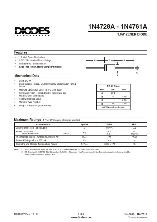
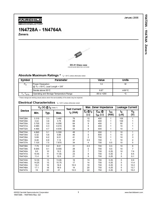
1N4728A - 1N4761A1.0W ZENEDIODENote: 1. Valid provided that leads are kept at T L @ 50°C with lead length = 9.5mm (3/8”) from case.2. EC Directive 2002/95/EC (RoHS) revision 13.2.2003. Glass and High Temperature Solder Exemptions Applied where applicable,see EU Directive Annex Notes 5 and 7.Mechanical Data·1.0 Watt Power Dissipation · 3.3V - 75V Nominal Zener Voltage ·Standard V Z Tolerance is 5%·Lead Free Finish, RoHS Compliant (Note 2)·Case: DO-41·Case Material: Glass. UL Flammability Classification Rating 94V-0·Moisture Sensitivity: Level 1 per J-STD-020C ·Terminals: Finish ¾ Sn96.5Ag3.5. Solderable per MIL-STD-202, Method 208·Polarity: Cathode Band ·Marking: Type Number·Weight: 0.35 grams (approximate)FeaturesElectrical Characteristics @ T A = 25°C unless otherwise specifiedNotes: 3. Measured under thermal equilibrium and dc (I ZT) test conditions.4. The Zener impedance is derived from the 60 Hz ac voltage which results when an ac current having an rms value equal to10% of the Zener current (I ZT or I ZK) is superimposed on I ZT or I ZK. Zener impedance is measured at two points to insure asharp knee on the breakdown curve and to eliminate unstable units.Notes: 5. *Add "-A" or "-T" to the appropriate type number in Table 1. Example: 6.2V Zener = 1N4735A-A for ammo pack. 6. For packaging details, visit our website at /datasheets/ap02008.pdf00.20.40.60.81.004080120160200P , T O T A L P O W E R D I S S I P A T I O N (W )d T , AMBIENT TEMPERATURE ( C)A Fig.1 Power Dissipation vs Ambient Temperature0250515202530l, Lead Length (mm)Fig. 2 Typical Thermal Resistance vs. Lead Length10200501001501101001000110100V , ZENER VOLTAGE (V)Z Fig. 4 Typical Zener Impedance vs. Zener Voltage1101001000102030405060C ,D I O DE C A P A C I T A N C E (pF )j V , ZENER VOLTAGE (V)Z Fig.3, Junction Capacitance vs Zener Voltagef = 1MHz T = 25CA V = 0V R V = 2V R V = 5V R V = 20VR V = 30VR Ordering Information(Note 6)IMPORTANT NOTICEDiodes Incorporated and its subsidiaries reserve the right to make modifications, enhancements, improvements, corrections or other changes without further notice to any product herein. Diodes Incorporated does not assume any liability arising out of the application or use of any product described herein; neither does it convey any license under its patent rights, nor the rights of others. The user of products in such applications shall assume all risks of such use and will agree to hold Diodes Incorporated and all the companies whose products are represented on our website, harmless against all damages.LIFE SUPPORTDiodes Incorporated products are not authorized for use as critical components in life support devices or systems without the expressed written approval of the President of Diodes Incorporated.。
473贴片电阻-概述说明以及解释
473贴片电阻-概述说明以及解释1.引言1.1 概述贴片电阻是一种常用的电子元件,广泛应用于电路板和电子设备中。
它是一种小型、方便安装和焊接的表面贴装电阻,具有较高的稳定性和精确的阻值。
相比传统的插件电阻,贴片电阻具有体积小、重量轻、可靠性高等优点。
贴片电阻的工作原理很简单,它通过电阻材料的阻值来限制电流的流动。
当电流通过贴片电阻时,会产生与电阻值成正比的电压降。
在电子电路中,贴片电阻常用于调节、分压、限流等功能。
在电子行业中,贴片电阻有着广泛的种类和规格。
根据其尺寸不同,常见的贴片电阻尺寸有0603、0805、1206等。
这些数字代表了电阻的长宽尺寸,比如0603表示长度为0.06英寸、宽度为0.03英寸。
此外,贴片电阻还有不同的阻值范围可供选择,从几欧姆到几兆欧姆都有。
贴片电阻在各个领域都有广泛的应用。
在通信领域,贴片电阻常用于通信设备和无线电设备中,起到信号传输和干扰抑制的作用。
在消费电子产品中,贴片电阻被广泛应用于手机、电视、音响等电子设备中,保证设备的正常运行和高品质音视频效果。
此外,贴片电阻还用于计算机、医疗器械、汽车电子等行业,为各种电子设备提供稳定的电阻功能。
综上所述,贴片电阻作为一种重要的电子元件,具有小巧、稳定、精确的特点,广泛应用于通信、消费电子、计算机等领域。
随着电子技术的不断发展,贴片电阻将继续发挥重要作用,并在尺寸、功耗、阻值范围等方面不断创新和改进。
因此,对于工程师和电子爱好者而言,深入了解和掌握贴片电阻的相关知识是非常有必要的。
1.2文章结构文章结构部分内容可以如下编写:文章结构:本文将围绕着473贴片电阻展开讨论,文章主要分为引言、正文和结论三大部分。
引言部分将首先对贴片电阻进行概述,介绍其定义、原理和应用领域等基本信息,为读者提供一个整体的认识和理解基础。
接着,文章将详细介绍本文的结构,即各个章节的内容安排和主要讨论的点,以便读者可以清楚地了解文章的组织结构和主旨。
BD4723资料
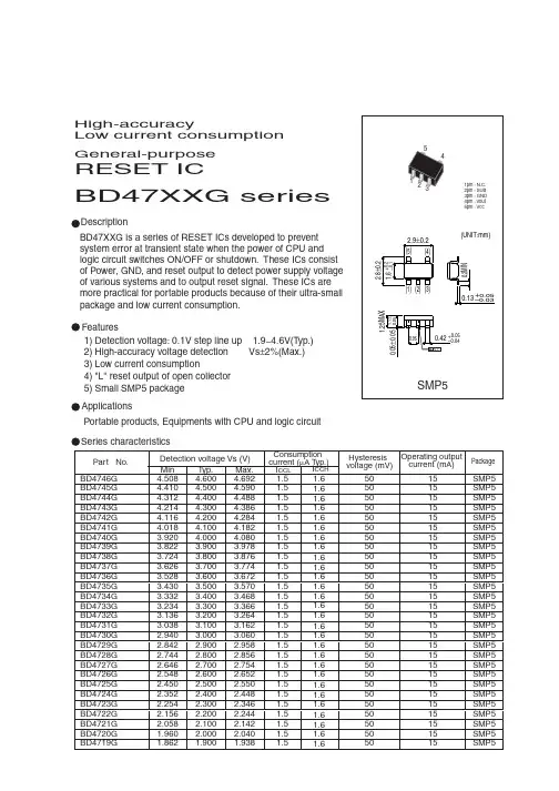
BD47XXG seriesHigh-accuracyLow current consumption BD47XXG is a series of RESET ICs developed to prevent system error at transient state when the power of CPU and logic circuit switches ON/OFF or shutdown. These ICs consist of Power, GND, and reset output to detect power supply voltage of various systems and to output reset signal. These ICs are more practical for portable products because of their ultra-small package and low current consumption.Description1) Detection voltage: 0.1V step line up 1.9~4.6V(Typ.)2) High-accuracy voltage detection Vs ±2%(Max.)3) Low current consumption4) "L" reset output of open collector 5) Small SMP5 package FeaturesPortable products, Equipments with CPU and logic circuit ApplicationsSeries characteristicsGeneral-purposeRESET ICAbsolute Maximum Ratings(Ta=25˚C)Application Circuit*2 TPHL : Vcc=(Vs typ.+0.4V)Æ(Vs typ.–0.4V)Electrical characteristics Timing waveform Transfer delay time measurement circuitVCCVOUTVS0V VS+VCCNote) The ratings shown above indicate breakdown limit of the pin and should not be regarded as the values that guarantee the operation.* Derating : 1.5mW/˚C for operation above Ta=25˚CCharacteristic diagram and Measurement circuit (When BD4729G is measured.)I c c (µA )Vcc (V)Current consumptionOperating limit voltage'L' output currentI/O characteristicNCV o u t (V )Vcc (V)V o u t (m V )Vcc (V)V o u t (m V )Iol (mA)Setting of the RESET signal delay timeDelay time can be set by capacitor C L and resistance R L connected to the output pin as shown below.CL is charged by R L when Vcc is rising. The delay time caused by charging is determined by thetime constant of C L, R L and the threshold voltage of RESET pin. RESET IC discharges C L forcedly when Vcc is falling. The delay time of RESET signal is determined by adding the delay time of single RESET IC to each time.VCCRESET(=VOUT)VS0VVOLVS+Marking Voltage Part No.Part No.Part No.Marking MarkingVoltage VoltageBD4719BABBBCBDBEBFBGBHB3BJ1.9V2.0V2.1V2.2V2.3V2.4V2.5V2.6V2.7V2.8VBKBLBMBNB4BPBQBRBSBT2.9V3.0V3.1V3.2V3.3V3.4V3.5V3.6V3.7V3.8VBUBVBWBXBYBZB1B23.9V4.0V4.1V4.2V4.3V4.4V4.5V4.6VBD4729BD4720BD4721BD4722BD4723BD4724BD4725BD4726BD4727BD4728BD4730BD4731BD4732BD4733BD4734BD4735BD4736BD4737BD4738BD4739BD4740BD4741BD4742BD4743BD4744BD4745BD4746 Part number and Marking of samplesAppendixAbout Export Control Order in JapanProducts described herein are the objects of controlled goods in Annex 1 (Item 16) of Export Trade ControlOrder in Japan.In case of export from Japan, please confirm if it applies to "objective" criteria or an "informed" (by MITI clause)on the basis of "catch all controls for Non-Proliferation of Weapons of Mass Destruction.Appendix1-Rev1.0。
JB4732钢制压力容器分析设计应力分类过程简介[1]
![JB4732钢制压力容器分析设计应力分类过程简介[1]](https://uimg.taocdn.com/40e063b2102de2bd97058836.webp)
(4)对于线性化后的应力根据标准释义中的相关规定 区分一次总体薄膜应力,一次局部薄膜应力,一次弯 曲应力,二次应力和峰值应力,并分别校核;
JB4732钢制压力容器分析设计应力分类过程简介
10
实例:球形封头裙座应力分析
校核线0-0通过筒体最大应力处,方向沿壁厚方向,远 离结构不连续处。
圆筒壳体薄膜应力理论解: Pm=PR/S =146.7MPa 与有限元结果相对误差为2.7%
球壳薄膜应力理论解: Pm=PR/2S =122.1MPa 与有限元结果相对误差为0.2%
路径
MEMBRANE
MEM+BEND
0-0
150.6
JB4732钢制压力容器分析设计应力分类过程简介
3
(一)一次应力 P
——平衡外加机械载荷所必须的应力 基本特征:非自限性
一次总体薄膜应力Pm 容器总体范围内存在 一次弯曲应力Pb 沿壁厚成线性分布的应力 一次局部薄膜应力PL
在结构不连续区产生的薄膜应力 JB4732钢制压力容器分析设计应力分类过程简介
图1 反应器结构简图 JB4732钢制压力容器分析设计应力分类过程简介
图2 裙座应力计算模型
11
应力分析结果:
(JB4732采用第三强度理论)
0-0
1-1
JB4732钢制压力容器分析设计应力分类过程简介
12
校核线1-1:
校核线1-1通过球壳与筒体连接位置,方向沿壁厚方向。 此处由于结构连续可能会产生较大的应力强度。之后 对校核线的应力分布做等效线性化处理。
(5)
峰值应力强度 S (由P +P Ⅴ JB4732钢制压力容器分析设计应力分类过程简介
IN4732A中文资料
For BZXyy series: Voltage rating 5.0 Third Line: Device name - For 1Nxx series: 7th to 8th characters of the device name.
4.085
4.3
4.515
4.465
4.7
4.935
4.845
5.1
5.355
5.32
5.6
5.88
5.89
6.2
6.51
6.46
6.8
7.14
7.125
7.5
7.875
7.79
8.2
8.61
8.645
9.1
9.555
9.5
10
10.5
10.45
11
11.55
11.4
12
12.6
12.35
13
13.65
1N4753A 1N4754A 1N4755A 1N4756A 1N4757A
1N4758A 1N4759A 1N4760A 1N4761A 1N4762A
1N4763A 1N4764A
Line 1
LOGO LOGO LOGO LOGO LOGO
LOGO LOGO LOGO LOGO LOGO
LOGO LOGO LOGO LOGO LOGO
1N4733A 1N4734A 1N4735A 1N4736A 1N4737A
BK4832规格书V0.2
BK4832 对讲机射频功率放大器 1 概述BK4832 是一款单片集成的高增益、高效率 的射频功率放大器芯片。
DL473-1992大直径三通锻件技术条件(pdf 6页)
4.9 超声波检查
6.3 / 4.9.1 超声波探伤应在锻件最终热处理后进行,探测工作表面的粗糙度为 ∇ 。
4.9.2 锻件经超声波检查,单个缺陷等级为Ⅱ级,密集区缺陷等级为Ⅰ级,低波降低量不得 超过Ⅰ级。
5 试验方法
5.1 锻件化学分析用试样的采取按三通锻件在三个端面各取一个试样,筒形锻件在两个端面
告和无损探伤报告等资料。
4.8 金相检查 4.8.1 锻件应不存在白点。 4.8.2 锻件材料中的非金属夹杂物采用 GB10561 评级图Ⅱ,A、B、C 和 D 四类夹杂物均不 大于 2 级。 4.8.3 锻件的晶粒度不低于 4 级,且级差不大于 3 级。 4.8.4 锻件的金相组织不允许有部分超过 AC1 的回火组织,对 12Cr1MoV 不允许有黄块马氏 体组织。
中华人民共和国电力行业标准 大直径三通锻件技术条件
DL 473-92
中华人民共和国能源部 1992-06-30 批准
1992-12-01 实施
1 主题内容与适用范围 本技术条件规定了大直径三通锻件的订货条件、技术要求、试验方法和验收。 本标准适用于管道公称外径不小于 400mm 的 300MW 及以上火力发电机组管道三通锻
S
P
Cr Mo
V Cu Ni
0.08~ 0.30~
≤ ≤ 2.00~ 0.90~
≤≤
12Cr2Mol
≤0.50
—
0.15 0.60
0.030 0.030 2.50 1.10
0.20 0.30
0.08~ 0.40~ 0.17~ ≤ ≤ 0.90~ 0.25~ 0.15~ ≤ ≤ 12Cr1MoV
0.15 0.70 0.37 0.035 0.035 1.20 0.35 0.30 0.20 0.30
JB4730.2射线检测__在实际工作中的应用
3.5焦距F;沿射线束中心测定的射线源与胶 片之间的距离。 (1)理解;F=f+b (2)应用;计算曝光量,采用其它方式透照 环向对接接头 (3)注意当用X射线机时要考虑窗口到焦点 的距离。
3.6射线源尺寸d;射线源的有效焦点尺寸 (1)理解;X光机所提供的焦点尺寸是有效 焦点尺寸 (2)应用;计算几何不清晰度 (3)注意;采用γ射线两个以上源叠加时以 长轴计算
• ②(纵缝)双壁透照:同上。 • ③椭圆形封头拼接缝透照(纵缝单壁内透照): 三次周向曝光 N= L’eff /250+2L”eff/250 L’eff=2(0.42Di+0.47T) L”eff=0.19 Di+1.1T+H 说明:N—透照片数;T—母材厚度;H—直边高度 f1min=0.57Di , f1max=0.9Di f2min=0.17Di f2min=0.31Di +0.79T , Di—封头齐边处焊缝内侧间的弦长,当拼缝经过封头 的顶点时,为该封头的公称直径。
3.11小径管;外直径D0小于或等于100mm的 管子 (1)理解;小径管外直径的上限为100mm, 下限无规定但壁厚≥2mm。(6.1.1) (2)应用;计算小径管的透照次数。 (3)注意;由于结构原因不能进行多次透照 时,应采取有效措施扩大缺陷的检出范围
3.12底片评定范围;本部分规定底片上必须 观测和评定的范围 (1)理解;以两搭接标记之间的距离为长, 焊缝加焊缝两侧热影响区为宽的范围。对 小径管而言应是黑度大于1.5(AB级)或黑 度大于大于2.0(B级)部分 (2)应用;评片时评定范围以外的缺陷不作 为该片的评定依据,但要在备注栏中注明。 当缺陷延伸到评定范围以外时也应计算其 尺寸和数量。 (3)注意;丁字焊口的纵、环部分焊缝也应 进行评定。
LM4732资料
LM4732Stereo 50W Audio Power Amplifier with MuteGeneral DescriptionThe LM4732is a stereo audio amplifier capable of typically delivering 50W per channel of continuous average output power into a 4Ωor 8Ωload with less than 10%THD+N from 20Hz -20kHz.The LM4732has short circuit protection and a thermal shut down feature that is activated when the die temperature exceeds 150˚C.The LM4732also has an under voltage lock out feature for click and pop free power on and off.Each amplifier of the LM4732has an independent smooth transition fade-in/out mute.The LM4732has a wide operating supply range from +/-10V -+/-40V allowing for lower cost unregulated power supplies to be used.The LM4732amplifiers can easily be configured for bridge or parallel operation for 100W mono solutions.Key Specificationsj Output Power/Channel at 10%THD+N,1kHz into 4Ωor 8Ω50W (typ)j THD+N at 2x 1W into 8Ω,1kHz 0.01%(typ)j Mute Attenuation 110dB (typ)j PSRR 89dB (typ)j Slew Rate19V/µs (typ)Featuresn Low external component count n Quiet fade-in/out mute mode n Wide supply range:20V -80VApplicationsn Audio amplifier for component stereo n Audio amplifier for compact stereon Audio amplifier for self-powered speakers n Audioamplifierforhigh-end and HD TVsTypical Application20072422FIGURE 1.Typical Audio Amplifier Application CircuitJuly 2003LM4732Stereo 50W Audio Power Amplifier with Mute©2003National Semiconductor Corporation Connection DiagramsPlastic Package (Note 13)200724D7Top ViewOrder Number LM4732TA See NS Package Number TA27ATO-220Top Marking200724D6Top ViewU -Wafer Fab Code Z -Assemble Plant CodeXY -Date CodeTT -Die Run Traceability L4732TA -LM4732TAL M 4732 2Absolute Maximum Ratings(Notes1, 2)If Military/Aerospace specified devices are required, please contact the National Semiconductor Sales Office/ Distributors for availability and specifications.Supply Voltage|V+|+|V-|80V Common Mode Input Voltage(V+or V-)and|V+|+|V-|≤80V Differential Input Voltage(Note12)60V Output Current Internally Limited Power Dissipation(Note3)125W ESD Susceptability(Note4) 3.0kV ESD Susceptability(Note5)200V Junction Temperature(T JMAX)(Note9)150˚CSoldering InformationTA Package(10seconds)260˚C Storage Temperature-40˚C to+150˚C Thermal ResistanceθJA30˚C/W θJC0.8˚C/W Operating Ratings(Notes1,2) Temperature RangeT MIN≤T A≤T MAX−20˚C≤T A≤+85˚C Supply Voltage|V+|+|V-|20V≤V TOTAL≤80VElectrical Characteristics(Notes1,2)The following specifications apply for V+=+29V,V-=−29V,I MUTE=-1mA/Channel and R L=8Ωunless otherwise specified. Limits apply for T A=25˚C.Symbol Parameter Conditions LM4732Units(Limits)Typical Limit(Note6)(Notes7,8)|V+|+|V-|Power Supply Voltage(Note10)V PIN7−V-≥9V182080V(min)V(max)A M Mute Attenuation I MUTE=0mA110dBP O Output Power(RMS)THD+N=10%(max),f=1kHz|V+|=|V-|=22V,R L=4Ω|V+|=|V-|=29V,R L=8Ω50504545W(min)W(min) THD+N=1%(max),f=1kHz|V+|=|V-|=22V,R L=4Ω|V+|=|V-|=29V,R L=8Ω4242WWTHD+N Total Harmonic Distortion+NoiseP O=1W,f=1kHzA V=26dB|V+|=|V-|=22V,R L=4Ω|V+|=|V-|=29V,R L=8Ω0.020.01%%X talk Channel Separation(Note11)P O=10W,f=1kHz70dB P O=10W,f=10kHz72dBSR Slew Rate V IN=2.0V P-P,t RISE=2ns19V/µsI DD Total Quiescent Power V CM=0V,105170mA(max)Supply Current V O=0V,I O=0AV OS Input Offset Voltage V CM=0V,I O=0mA110mV(max) I B Input Bias Current V CM=0V,I O=0mA0.2µAPSRR Power Supply Rejection Ratio V EE=-29V+V RIPPLE=1V RMSf RIPPLE=120Hz sine wave,V CC=29V DC62dB V CC=29V+V RIPPLE=1V RMSf RIPPLE=120Hz sine wave,V EE=-29V DC89dBA VOL Open Loop Voltage Gain R L=2kΩ,∆V O=40V115dBe IN Input Noise IHF-A-Weighting Filter,R IN=600Ω(Input Referred)2.0µVNote1:All voltages are measured with respect to the ground pins,unless otherwise specified.Note2:Absolute Maximum Ratings indicate limits beyond which damage to the device may occur.Operating Ratings indicate conditions for which the device is functional,but do not guarantee specific performance limits.Electrical Characteristics state DC and AC electrical specifications under particular test conditions which guarantee specific performance limits.This assumes that the device is within the Operating Ratings.Specifications are not guaranteed for parameters where no limit is given;however,the typical value is a good indication of device performance.LM47323Electrical Characteristics (Notes 1,2)(Continued)Note 3:The maximum power dissipation must be de-rated at elevated temperatures and is dictated by T JMAX ,θJC ,and the ambient temperature T A .The maximum allowable power dissipation is P DMAX =(T JMAX -T A )/θJC or the number given in the Absolute Maximum Ratings,whichever is lower.For the LM4732,T JMAX =150˚C and the typical θJC is 0.8˚C/W.Refer to the Thermal Considerations section for more information.Note 4:Human body model,100pF discharged through a 1.5k Ωresistor.Note 5:Machine Model:a 220pF -240pF discharged through all pins.Note 6:Typical specifications are measured at 25˚C and represent the parametric norm.Note 7:Tested limits are guaranteed to National’s AOQL (Average Outgoing Quality Level).Note 8:Datasheet min/max specification limits are guaranteed by design,test,or statistical analysis.Note 9:The maximum operating junction temperature is 150˚C.However,the instantaneous Safe Operating Area temperature is 250˚C.Note 10:V -must have at least -9V at its pin with reference to GND in order for the under-voltage protection circuitry to be disabled.In addition,the voltage differential between V +and V -must be greater than 14V.Note 11:Cross talk performance was measured using the demo board shown in the datasheet.PCB layout will affect cross talk.It is recommended that input and output traces be separated by as much distance as possible.Return ground traces from outputs should be independent back to a single ground point and use as wide of traces as possible.Note 12:The Differential Input Voltage Absolute Maximum Rating is based on supply voltages V +=40V and V -=-40V.Note 13:The TA27A is a non-isolated package.The package’s metal back,and any heat sink to which it is mounted are connected to the V -potential when using only thermal compound.If a mica washer is used in addition to thermal compound,θCS (case to sink)is increased,but the heat sink will be electrically isolated from V -.Note 14:CCIR/ARM:A Practical Noise Measurement Method;by Ray Dolby,David Robinson and Kenneth Gundry,AES Preprint No.1353(F-3).L M 4732 4LM4732 Bridged Amplifier Application Circuit20072414FIGURE2.Bridged Amplifier Application Circuit5Parallel Amplifier Application Circuit20072413FIGURE 3.Parallel Amplifier Application CircuitL M 4732 6Single Supply Application CircuitNote:*Optional components dependent upon specific design requirements.Auxiliary Amplifier Application Circuit20072406FIGURE 4.Single Supply Amplifier Application Circuit200724D5FIGURE 5.Special Audio Amplifier Application CircuitLM47327External Components Description(Figures 1-5)Components Functional Description1R BPrevents current from entering the amplifier’s non-inverting input.This current may pass through to the load during system power down,because of the amplifier’s low input impedance when the undervoltage circuitry is off.This phenomenon occurs when the V +and V -supply voltages are below 1.5V.2R i Inverting input resistance.Along with R f ,sets AC gain.3R fFeedback resistance.Along with R i ,sets AC gain.4R f2(Note 15)Feedback resistance.Works with Cf and Rf creating a lowpass filter that lowers AC gain at high frequencies.The -3dB point of the pole occurs when:(R f -R i )/2=R f //[1/(2πf c C f )+R f2]for the Non-Inverting configuration shown in Figure 5.5C f(Note 15)Compensation capacitor.Works with R f and R f2to reduce AC gain at higher frequencies.6C C(Note 15)Compensation capacitor.Reduces the gain at higher frequencies to avoid quasi-saturation oscillations of the output transistor.Also suppresses external electromagnetic switching noise created from fluorescent lamps.7C i(Note 15)Feedback capacitor which ensures unity gain at DC.Along with R i also creates a highpass filter at f c =1/(2πR i C i ).8C SProvides power supply filtering and bypassing.Refer to the Supply Bypassing application section for proper placement and selection of bypass capacitors.9R V(Note 15)Acts as a volume control by setting the input voltage level.10R IN(Note 15)Sets the amplifier’s input terminals DC bias point when C IN is present in the circuit.Also works with C IN to create a highpass filter at f C =1/(2πR IN C IN ).If the value of R IN is too large,oscillations may be observed on the outputs when the inputs are floating.Recommended values are 10k Ωto 47k Ω.Refer to Figure 5.11C IN(Note 15)Input capacitor.Prevents the input signal’s DC offsets from being passed onto the amplifier’s inputs.12R SN(Note 15)Works with C SN to stabilize the output stage by creating a pole that reduces high frequency instabilities.13C SN(Note 15)Works with R SN to stabilize the output stage by creating a pole that reduces high frequency instabilities.The pole is set at f C =1/(2πR SN C SN ).Refer to Figure 5.14L (Note 15)Provides high impedance at high frequencies so that R may decouple a highly capacitive load and reduce the Q of the series resonant circuit.Also provides a low impedance at low frequencies to short out R and pass audio signals to the load.Refer to Figure 5.15R (Note 15)16R A Provides DC voltage biasing for the transistor Q1in single supply operation.17C AProvides bias filtering for single supply operation.18R INP(Note 15)Limits the voltage difference between the amplifier’s inputs for single supply operation.Refer to the Clicks and Pops application section for a more detailed explanation of the function of R INP .19R BI Provides input bias current for single supply operation.Refer to the Clicks and Pops application section for a more detailed explanation of the function of R BI .20R E Establishes a fixed DC current for the transistor Q1in single supply operation.This resistor stabilizes the half-supply point along with C A .21R MMute resistance set up to allow 0.5mA to be drawn from each MUTE pin to turn the muting function off.→R M is calculated using:R M ≤(|V EE |−2.6V)/l where l ≥0.5mA.Refer to the Mute Attenuation vs Mute Current curves in the Typical Performance Characteristics section.22C M Mute capacitance set up to create a large time constant for turn-on and turn-off muting.23S 1Mute switch.When open or switched to GND,the amplifier will be in mute mode.24R OUTReduces current flow between outputs that are caused by Gain or DC offset differences between the amplifiers.Note 15:Optional components dependent upon specific design requirements.L M 4732 8Optional External Component InteractionThe optional external components have specific desired functions.Their values are chosen to reduce the bandwidth and eliminate unwanted high frequency oscillation.They may,however,cause certain undesirable effects when they interact.Interaction may occur when the components pro-duce reactions that are nearly equal to one another.One example is the coupling capacitor,C C,and the compensa-tion capacitor,C f.These two components are low imped-ances at certain frequencies.They may couple signals from the input to the output.Please take careful note of basic amplifier component functionality when selecting the value of these components and their placement on a printed circuit board(PCB).The optional external components shown in Figure4and Figure5,and described above,are applicable in both single and split supply voltage configurations.Typical Performance CharacteristicsSupply Current vs Supply VoltagePSRR vs Frequency±29V,VRIPPLE=1V RMSR L=8Ω,80kHz BW200724E5200724E4THD+N vs Frequency ±22V,POUT=1W/Channel R L=4Ω,80kHz BWTHD+N vs Frequency±29V,POUT=1W/ChannelR L=8Ω,80kHz BW200724D8200724E6LM4732 9Typical Performance Characteristics(Continued)THD+N vs Output Power/Channel±22V,R L =4Ω,80kHz BWTHD+N vs Output Power/Channel±29V,R L =8Ω,80kHz BW200724F0200724F1Output Power/Channel vs Supply Voltagef =1kHz,R L =4Ω,80kHz BW Output Power/Channel vs Supply Voltagef =1kHz,R L =8Ω,80kHz BW200724E2200724E3Total Power Dissipation vs Output Power/Channel1%THD (max),R L =4Ω,80kHz BW Total Power Dissipation vs Output Power/Channel1%THD (max),R L =8Ω,80kHz BW200724F3200724D9L M 4732 10Typical Performance Characteristics(Continued)Crosstalk vs Frequency ±22V,P OUT =10W R L =4Ω,80kHz BWCrosstalk vs Frequency ±29V,P OUT =10W R L =8Ω,80kHz BW200724C5200724A5Mute Attenuation vs Mute Pin Current P OUT =10W/ChannelCommon Mode Rejection Ratio200724C6200724C9THD+N vs Frequency ±22V,P OUT =1W &50WBridge Mode (Note 16),R L =8Ω,80kHz BW THD+N vs Frequency ±29V,P OUT =1W &50WParallel Mode (Note 17),R L =4Ω,80kHz BW200724E8200724E9LM473211Typical Performance Characteristics(Continued)THD+N vs Output Power±22V,Bridge Mode (Note 16)R L =8Ω,80kHz BWTHD+N vs Output Power±29V,Parallel Mode (Note 17)R L =4Ω,80kHz BW200724F2200724E7Output Power vsSupply Voltage,Bridge Mode (Note 16)f =1kHz,R L =8Ω,80kHz BW Output Power vsSupply Voltage,Parallel Mode (Note 17)f =1kHz,R L =4Ω,80kHz BW200724E0200724E1Note 16:Bridge mode graphs were taken using the demo board and inverting the signal to the channel B input.Note 17:Parallel mode graphs were taken using the demo board and connecting each output through a 0.1Ω/3W resistor to the load.L M 4732 12Application InformationMUTE MODEThe muting function allows the user to mute the amplifier. This can be accomplished as shown in the Typical Applica-tion Circuit.The resistor R M is chosen with reference to the negative supply voltage and is used in conjunction with a switch.The switch,when opened or switched to GND,cuts off the current flow from the MUTE pins to−V EE,thus placing the LM4732into mute mode.Refer to the Mute Attenuation vs Mute Current curves in the Typical Performance Char-acteristics section for values of attenuation per current out of each MUTE pin.The resistance R M is calculated by the following equation:R M≤(|−V EE|−2.6V)/I MUTEWhere I MUTE≥0.5mA for each MUTE pin.The MUTE pins can be tied together so that only one resistor is required for the mute function.The mute resistor value must be chosen so that a minimum of1mA is pulled through the resistor R M.This ensures that each amplifier is fully operational.Taking into account supply line fluctuations,it is a good idea to pull out1mA per MUTE pin or2mA total if both pins are tied together.A turn-on MUTE or soft start circuit may also be used during power up.A simple circuit like the one shown below may be used.200724A3The RC combination of C M and R M1may cause the voltage at point A to change more slowly than the-V EE supply voltage.Until the voltage at point A is low enough to have 0.5mA of current per MUTE pin flow through R M2,the IC will be in mute mode.The series combination of R M1and R M2 needs to satisfy the mute equation above for all operating voltages or mute mode may be activated during normal operation.For a longer turn-on mute time,a larger time constant,τ=RC=R M1C M(sec),is needed.For the values show above and with the MUTE pins tied together,the LM4732will enter play mode when the voltage at point A is -17.6V.The voltage at point A is found with Equation(1) below.V A(t)=(V f-V O)e-t/τ(Volts)(1) where:t=time(sec)τ=RC(sec)V o=Voltage on C at t=0(Volts)V f=Final voltage,-V EE in this circuit(Volts)UNDER-VOLTAGE PROTECTIONUpon system power-up,the under-voltage protection cir-cuitry allows the power supplies and their corresponding capacitors to come up close to their full values before turning on the LM4732.Since the supplies have essentially settled to their final value,no DC output spikes occur.At power down,the outputs of the LM4732are forced to ground before the power supply voltages fully decay preventing transients on the output.OVER-VOLTAGE PROTECTIONThe LM4732contains over-voltage protection circuitry thatlimits the output current while also providing voltage clamp-ing.The clamp does not,however,use internal clampingdiodes.The clamping effect is quite the same because theoutput transistors are designed to work alternately by sinkinglarge current spikes.THERMAL PROTECTIONThe LM4732has a sophisticated thermal protection schemeto prevent long-term thermal stress of the device.When thetemperature on the die exceeds150˚C,the LM4732shutsdown.It starts operating again when the die temperaturedrops to about145˚C,but if the temperature again begins torise,shutdown will occur again above150˚C.Therefore,thedevice is allowed to heat up to a relatively high temperatureif the fault condition is temporary,but a sustained fault willcause the device to cycle in a Schmitt Trigger fashion be-tween the thermal shutdown temperature limits of150˚C and145˚C.This greatly reduces the stress imposed on the IC bythermal cycling,which in turn improves its reliability undersustained fault conditions.Since the die temperature is directly dependent upon theheat sink used,the heat sink should be chosen so thatthermal shutdown is not activated during normal operation.Using the best heat sink possible within the cost and spaceconstraints of the system will improve the long-term reliabilityof any power semiconductor device,as discussed in theDetermining the Correct Heat Sink section.DETERMlNlNG MAXIMUM POWER DISSIPATIONPower dissipation within the integrated circuit package is avery important parameter requiring a thorough understand-ing if optimum power output is to be obtained.An incorrectmaximum power dissipation calculation may result in inad-equate heat sinking causing thermal shutdown and thuslimiting the output power.Equation(2)shows the theoretical maximum power dissipa-tion point of each amplifier in a single-ended configurationwhere V CC is the total supply voltage.P DMAX=(V CC)2/2π2R L(2) Thus by knowing the total supply voltage and rated outputload,the maximum power dissipation point can be calcu-lated.The package dissipation is twice the number whichresults from Equation(2)since there are two amplifiers ineach LM4732.Refer to the graphs of Power Dissipationversus Output Power in the Typical Performance Charac-teristics section which show the actual full range of powerdissipation not just the maximum theoretical point that re-sults from Equation(2).DETERMINING THE CORRECT HEAT SINKThe choice of a heat sink for a high-power audio amplifier ismade entirely to keep the die temperature at a level suchthat the thermal protection circuitry is not activated undernormal circumstances.The thermal resistance from the die to the outside air,θJA(junction to ambient),is a combination of three thermal re-sistances,θJC(junction to case),θCS(case to sink),andθSA(sink to ambient).The thermal resistance,θJC(junction tocase),of the LM4732T is0.8˚C/ing Thermalloy Ther-macote thermal compound,the thermal resistance,θCS(case to sink),is about0.2˚C/W.Since convection heat flow(power dissipation)is analogous to current flow,thermalLM473213Application Information(Continued)resistance is analogous to electrical resistance,and tem-perature drops are analogous to voltage drops,the power dissipation out of the LM4732is equal to the following:P DMAX =(T JMAX −T AMB )/θJA (3)where T JMAX =150˚C,T AMB is the system ambient tempera-ture and θJA =θJC +θCS +θSA .20072452Once the maximum package power dissipation has been calculated using Equation (2),the maximum thermal resis-tance,θSA ,(heat sink to ambient)in ˚C/W for a heat sink can be calculated.This calculation is made using Equation (4)which is derived by solving for θSA in Equation (3).θSA =[(T JMAX −T AMB )−P DMAX (θJC +θCS )]/P DMAX (4)Again it must be noted that the value of θSA is dependent upon the system designer’s amplifier requirements.If the ambient temperature that the audio amplifier is to be working under is higher than 25˚C,then the thermal resistance for the heat sink,given all other things are equal,will need to be smaller.SUPPLY BYPASSINGThe LM4732has excellent power supply rejection and does not require a regulated supply.However,to improve system performance as well as eliminate possible oscillations,the LM4732should have its supply leads bypassed with low-inductance capacitors having short leads that are located close to the package terminals.Inadequate power supply bypassing will manifest itself by a low frequency oscillation known as “motorboating”or by high frequency instabilities.These instabilities can be eliminated through multiple by-passing utilizing a large tantalum or electrolytic capacitor (10µF or larger)which is used to absorb low frequency variations and a small ceramic capacitor (0.1µF)to prevent any high frequency feedback through the power supply lines.If adequate bypassing is not provided,the current in the supply leads which is a rectified component of the load current may be fed back into internal circuitry.This signal causes distortion at high frequencies requiring that the sup-plies be bypassed at the package terminals with an electro-lytic capacitor of 470µF or more.BRIDGED AMPLIFIER APPLICATIONThe LM4732has two operational amplifiers internally,allow-ing for a few different amplifier configurations.One of these configurations is referred to as “bridged mode”and involves driving the load differentially through the LM4732’s outputs.This configuration is shown in Figure 2.Bridged mode op-eration is different from the classical single-ended amplifier configuration where one side of its load is connected to ground.A bridge amplifier design has a distinct advantage over the single-ended configuration,as it provides differential drive to the load,thus doubling output swing for a specified supplyvoltage.Theoretically,four times the output power is pos-sible as compared to a single-ended amplifier under thesame conditions.This increase in attainable output power assumes that the amplifier is not current limited or clipped.A direct consequence of the increased power delivered to the load by a bridge amplifier is an increase in internal power dissipation.For each operational amplifier in a bridge con-figuration,the internal power dissipation will increase by a factor of two over the single ended dissipation.Thus,for an audio power amplifier such as the LM4732,which has two operational amplifiers in one package,the package dissipa-tion will increase by a factor of four.To calculate the LM4732’s maximum power dissipation point for a bridged load,multiply Equation (2)by a factor of four.This value of P DMAX can be used to calculate the correct size heat sink for a bridged amplifier application.Since the inter-nal dissipation for a given power supply and load is in-creased by using bridged-mode,the heatsink’s θSA will have to decrease accordingly as shown by Equation (4).Refer to the section,Determining the Correct Heat Sink,for a more detailed discussion of proper heat sinking for a given appli-cation.PARALLEL AMPLIFIER APPLICATIONParallel configuration is normally used when higher output current is needed for driving lower impedance loads (i.e.4Ωor lower)to obtain higher output power levels.As shown in Figure 3,the parallel amplifier configuration consist of de-signing the amplifiers in the IC to have identical gain,con-necting the inputs in parallel and then connecting the outputs in parallel through a small external output resistor.Any num-ber of amplifiers can be connected in parallel to obtain the needed output current or to divide the power dissipation across multiple IC packages.Ideally,each amplifier shares the output current equally.Due to slight differences in gain the current sharing will not be equal among all channels.If current is not shared equally among all channels then the power dissipation will also not be equal among all channels.It is recommended that 0.1%tolerance resistors be used to set the gain (R i and R f )for a minimal amount of difference in current sharing.When operating two or more amplifiers in parallel mode the impedance seen by each amplifier is equal to the total load impedance multiplied by the number of amplifiers driving the load in parallel as shown by Equation (5)below:R L(parallel)=R L(total)*Number of amplifiers(5)Once the impedance seen by each amplifier in the parallel configuration is known then Equation (2)can be used with this calculated impedance to find the amount of power dis-sipation for each amplifier.Total power dissipation (P DMAX )within an IC package is found by adding up the power dissipation for each amplifier in the IC ing the calculated P DMAX the correct heat sink size can be deter-mined.Refer to the section,Determining the Correct Heat Sink ,for more information and detailed discussion of proper heat sinking.SINGLE-SUPPLY AMPLIFIER APPLICATIONThe typical application of the LM4732is a split supply am-plifier.But as shown in Figure 4,the LM4732can also be used in a single power supply configuration.This involves using some external components to create a half-supply bias which is used as the reference for the inputs and outputs.Thus,the signal will swing around half-supply much like it swings around ground in a split-supply application.AlongL M 473214Application Information(Continued)with proper circuit biasing,a few other considerations must be accounted for to take advantage of all of the LM4732 functions,like the mute function.CLICKS AND POPSIn the typical application of the LM4732as a split-supply audio power amplifier,the IC exhibits excellent“click”and “pop”performance when utilizing the mute mode.In addition, the device employs Under-Voltage Protection,which elimi-nates unwanted power-up and power-down transients.The basis for these functions are a stable and constant half-supply potential.In a split-supply application,ground is the stable half-supply potential.But in a single-supply applica-tion,the half-supply needs to charge up at the same rate as the supply rail,V CC.This makes the task of attaining a clickless and popless turn-on more challenging.Any uneven charging of the amplifier inputs will result in output clicks and pops due to the differential input topology of the LM4732. To achieve a transient free power-up and power-down,the voltage seen at the input terminals should be ideally the same.Such a signal will be common-mode in nature,and will be rejected by the LM4732.In Figure4,the resistor R INP serves to keep the inputs at the same potential by limiting the voltage difference possible between the two nodes.This should significantly reduce any type of turn-on pop,due to an uneven charging of the amplifier inputs.This charging is based on a specific application loading and thus,the system designer may need to adjust these values for optimal perfor-mance.As shown in Figure4,the resistors labeled R BI help bias up the LM4732off the half-supply node at the emitter of the 2N3904.But due to the input and output coupling capacitors in the circuit,along with the negative feedback,there are two different values of R BI,namely10kΩand200kΩ.These resistors bring up the inputs at the same rate resulting in a popless turn-on.Adjusting these resistors values slightly may reduce pops resulting from power supplies that ramp extremely quick or exhibit overshoot during system turn-on. PROPER SELECTION OF EXTERNAL COMPONENTS Proper selection of external components is required to meet the design targets of an application.The choice of external component values that will affect gain and low frequency response are discussed below.The gain of each amplifier is set by resistors R f and R i for the non-inverting configuration shown in Figure1.The gain is found by Equation(6)below:A V=1+R f/R i(V/V)(6) For best noise performance,lower values of resistors are used.A value of1kΩis commonly used for R i and then setting the value of R f for the desired gain.For the LM4732 the gain should be set no lower than10V/V and no higher than50V/V.Gain settings below10V/V may experience instability and using the LM4732for gains higher than50V/V will see an increase in noise and THD.The combination of R i with C i(see Figure1)creates a high pass filter.The low frequency response is determined by these two components.The-3dB point can be found from Equation(7)shown below:f i=1/(2πR i C i)(Hz)(7) If an input coupling capacitor is used to block DC from the inputs as shown in Figure5,there will be another high pass filter created with the combination of C IN and R IN.Whenusing a input coupling capacitor R IN is needed to set the DCbias point on the amplifier’s input terminal.The resulting-3dB frequency response due to the combination of C IN andR IN can be found from Equation(8)shown below:f IN=1/(2πR IN C IN)(Hz)(8)With large values of R IN oscillations may be observed on theoutputs when the inputs are left floating.Decreasing thevalue of R IN or not letting the inputs float will remove theoscillations.If the value of R IN is decreased then the value ofC IN will need to increase in order to maintain the same-3dBfrequency response.HIGH PERFORMANCE CONSIDERATIONSUsing low cost electrolytic capacitors in the signal path suchas C IN and C i(see Figures1-5)will result in very goodperformance.However,electrolytic capacitors are less linearthan other premium capacitors.Higher THD+N performancemay be obtained by using high quality polypropylene capaci-tors in the signal path.A more cost effective solution may bethe use of smaller value premium capacitors in parallel withthe larger electrolytic capacitors.This will maintain signalquality in the upper audio band where any degradation ismost noticeable while also coupling in the signals in thelower audio band for good bass response.Distortion is introduced as the audio signal approaches thelower-3dB point,determined as discussed in the sectionabove.By using larger values of capacitors such that the-3dB point is well outside of the audio band will reduce thisdistortion and improve THD+N performance.Increasing the value of the large supply bypass capacitorswill improve burst power output.The larger the supply by-pass capacitors the higher the output pulse current withoutsupply droop increasing the peak output power.This will alsoincrease the headroom of the amplifier and reduce THD.SIGNAL-TO-NOISE RATIOIn the measurement of the signal-to-noise ratio,misinterpre-tations of the numbers actually measured are common.Oneamplifier may sound much quieter than another,but due toimproper testing techniques,they appear equal in measure-ments.This is often the case when comparing integratedcircuit designs to discrete amplifier designs.Discrete transis-tor amps often“run out of gain”at high frequencies andtherefore have small bandwidths to noise as indicated below.20072499Integrated circuits have additional open loop gain allowingadditional feedback loop gain in order to lower harmonicdistortion and improve frequency response.It is this addi-tional bandwidth that can lead to erroneous signal-to-noisemeasurements if not considered during the measurementprocess.In the typical example above,the difference inbandwidth appears small on a log scale but the factor of10inbandwidth,(200kHz to2MHz)can result in a10dB theoreti-cal difference in the signal-to-noise ratio(white noise isproportional to the square root of the bandwidth in a system).LM473215。
- 1、下载文档前请自行甄别文档内容的完整性,平台不提供额外的编辑、内容补充、找答案等附加服务。
- 2、"仅部分预览"的文档,不可在线预览部分如存在完整性等问题,可反馈申请退款(可完整预览的文档不适用该条件!)。
- 3、如文档侵犯您的权益,请联系客服反馈,我们会尽快为您处理(人工客服工作时间:9:00-18:30)。
BD47XXG series
High-accuracy
Low current consumption BD47XXG is a series of RESET ICs developed to prevent system error at transient state when the power of CPU and logic circuit switches ON/OFF or shutdown. These ICs consist of Power, GND, and reset output to detect power supply voltage of various systems and to output reset signal. These ICs are more practical for portable products because of their ultra-small package and low current consumption.
Description
1) Detection voltage: 0.1V step line up 1.9~4.6V(Typ.)2) High-accuracy voltage detection Vs ±2%(Max.)3) Low current consumption
4) "L" reset output of open collector 5) Small SMP5 package Features
Portable products, Equipments with CPU and logic circuit Applications
Series characteristics
General-purpose
RESET IC
Absolute Maximum Ratings(Ta=25˚C)
Application Circuit
*2 TPHL : Vcc=(Vs typ.+0.4V)Æ(Vs typ.–0.4V)
Electrical characteristics Timing waveform Transfer delay time measurement circuit
VCC
VOUT
VS
0V VS+VCC
Note) The ratings shown above indicate breakdown limit of the pin and should not be regarded as the values that guarantee the operation.
* Derating : 1.5mW/˚C for operation above Ta=25˚C
Characteristic diagram and Measurement circuit (When BD4729G is measured.)
I c c (µA )
Vcc (V)
Current consumption
Operating limit voltage
'L' output current
I/O characteristic
NC
V o u t (V )
Vcc (V)
V o u t (m V )
Vcc (V)
V o u t (m V )
Iol (mA)
Setting of the RESET signal delay time
Delay time can be set by capacitor C L and resistance R L connected to the output pin as shown below.
CL is charged by R L when Vcc is rising. The delay time caused by charging is determined by the
time constant of C L, R L and the threshold voltage of RESET pin. RESET IC discharges C L forcedly when Vcc is falling. The delay time of RESET signal is determined by adding the delay time of single RESET IC to each time.
VCC
RESET
(=VOUT)
VS
0V
VOL
VS+
Marking Voltage Part No.Part No.Part No.
Marking Marking
Voltage Voltage
BD4719
BA
BB
BC
BD
BE
BF
BG
BH
B3
BJ
1.9V
2.0V
2.1V
2.2V
2.3V
2.4V
2.5V
2.6V
2.7V
2.8V
BK
BL
BM
BN
B4
BP
BQ
BR
BS
BT
2.9V
3.0V
3.1V
3.2V
3.3V
3.4V
3.5V
3.6V
3.7V
3.8V
BU
BV
BW
BX
BY
BZ
B1
B2
3.9V
4.0V
4.1V
4.2V
4.3V
4.4V
4.5V
4.6V
BD4729
BD4720
BD4721
BD4722
BD4723
BD4724
BD4725
BD4726
BD4727
BD4728
BD4730
BD4731
BD4732
BD4733
BD4734
BD4735
BD4736
BD4737
BD4738
BD4739
BD4740
BD4741
BD4742
BD4743
BD4744
BD4745
BD4746 Part number and Marking of samples
Appendix
About Export Control Order in Japan
Products described herein are the objects of controlled goods in Annex 1 (Item 16) of Export Trade Control
Order in Japan.
In case of export from Japan, please confirm if it applies to "objective" criteria or an "informed" (by MITI clause)
on the basis of "catch all controls for Non-Proliferation of Weapons of Mass Destruction.
Appendix1-Rev1.0。