350JJ122U040C中文资料
HS3140B-4Q资料

30
40
50
VOS-mV
Additional Linearity Error vs. Output-Amplifier
Offset-Voltage (VREF = + 10V)
0.01 0.008
0.006
0.004
0.002
0
4
6
8
10
12
14
16
18
VDD -VOLTS
Gain Change vs. Supply Voltage
@ 1kHz @ 10kHz Reference Input Bandwidth
POWER SUPPLY (VDD) Operating Voltage Voltage Range Current Rejection Ratio
14 Binary
Offset Binary CMOS, TTL
±1
±25
2
© Copyright 2000 Sipex Corporation
元器件交易网
SPECIFICATIONS (continued)
(Typical @ 25°C, nominal power supply, VREF = +10V, unipolar unless otherwise noted)
VREF 19
15 EQUAL SECTIONS
96k
96k
3 GND
18 VDD
4 to 16 DECODE
4
5
6
7
BIT 1 BIT 2 BIT 3 BIT 4 (MSB)
SP7514S,PH7S5311440
48k
96k
96k
混凝土搅拌机型号及主要技术参数

混凝土搅拌机型号及主要技术参数JS是指:双卧轴强制式搅拌机500是指:出料容量该系列设备具备了可以单机独立作业和与PLD系列配料机组成简易式混凝土搅拌站的双重优越性,还可为搅拌站提供配套主机,适用于各类大、中、小预制构件厂及公路、桥梁、水利、码头等工业及民用建筑工程,可搅拌干硬性混凝土、塑性混凝土、流动性混凝土、轻骨料混凝土及各种砂浆,是一种高效率机型,应用非常广泛。
该系列产品设计结构合理,布局新颖,使用维修方便。
支腿部分高度设计为:JS500为1500mm,JS750为1600mm,JS1000为3500mm和4000mm,JS1500和JS2000为4500mm。
用户可自配翻斗车、自卸车、搅拌车使用,同时还可根据用户特殊要求进行改制,以满足用户需要。
主要技术参数项目参数型号JS500出料容量500L进料容量800L生产率25m3/h骨料最大料径(卵石/碎石)mm 80/60搅拌叶片转速35r/min 数量2×7搅拌电机型号Y180M-4 功率18.5kw卷扬电机型号YEZ132S-4-BS 功率 5.5kw水泵电机型号50DWB20-8A 功率750W料斗提升速度18m/min外形尺寸(长×宽×高)运输状态3050×2300×2680mm工作状态4461×3050×5225mm整机重量4000kg卸料高度1500mmJDY500D 是指:单卧轴强制式搅拌机单卧轴强制式搅拌机是一种新型多功能砼搅拌机械,该机使用范围广,可适用于豢塑性、干硬性、软骨料混凝土及各种灰浆、砂石的搅拌。
该机具有结构简单、搅拌质量好、生产效率高、能耗低、噪声小、寿命长、维修保养方便等优点。
适用于预制厂、公路、桥梁、码头等建筑工地。
本机除作单机使用外,还可与配料机组合成简易式搅拌站。
是您创优质工程的保证。
JDK500D主要技术参数:出料容量:500升,进料容量:800升,生产能力:25-30立方米/小时,整机质量:4500千克,整机功率:15.55KW,料斗提升速度:20米/分,搅拌轴转速:25转/分,搅拌时间:25-30秒,骨料粒径:60/80MM.外型尺寸:3300*2150*1870MM*JDY混凝土搅拌机有JDY350型,JDY350C型,JDY500型,JDY500D型。
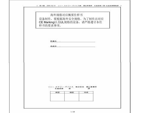
海外规格仕样书第4版(中文)
4.在机铭板上标示出以下内容 ・制造者名 ・制造年月 ・形式以及model编号 ・定格电源电压(电压、位相、周波数、最大负荷电流、etc) 在电源上不可以用「AC200V」表示,而要用「~200V」表示 ・气压(定格压力) ・原产地表示(MADE IN JAPAN等) 注)FA标准机铭板: 4—710—156—01(大—11) 带孔、by三立产业 EN60204 UL1740
8.盖子、马达框架、trans core、电装品筐体、以及接续管等的金属部, 如果和地线或金属接触,会导致和物品本身的导通。
EN60204、UL1740
7/28
要求事项
1.电源切断装置要使用得到认可的漏电断路器、自动断路器、线路保护器 EN60204、UL1740 2.主断路器的定格要遵循以下事项。 EN60204、UL1740 a)电流容量:最大负荷电流的115%以上,或者使用的导线的要求容许电流以下 (14配线以及电路——参照17) b)切断容量:在机器上使用的马达中,最大马达的 rotor rock电流+其他装置的 最大负荷电流以上 3.电力引入线(一次电源)要直接和断路器连接 EN60204、UL1740 4.电源切断装置遵循一下事项。 EN60204、UL1740 (a)安装把手,方便从外部操作 (b)把手的中心高度在0.6~1.9以内 (c)要有OFF锁定机能.(可以上锁的构造) (d)门关上时要有ON/OFF的明确指示 (e)ON/OFF可以用「O」也可以用「I」来表示 (f)接地导线以外所有的相要同时切断 (g)主断路器上如果没有OFF锁定机能,要在负荷侧设定带钥匙的主开关。
贵社 check
本社 check
备注
① 外 观 以 及 构 造 的 规 定
4/28
KYORITSU 4105A Digital Earth Resistance Tester 说明书

INSTRUCTION MANUALMODEL 4105A KYORITSU ELECTRICAL INSTRUMENTSWORKS, LTD.CONTENTS1. Safety Precautions (1)2. Features (4)3. Specifications (5)4. Layout Diagram (8)5. Preparation for Measurement (9)5-1 Battery Voltage Check (9)5-2 Connecting Test Probes (9)6. Operating Instructions (9)6-1 Principle of Measurement (9)6-2 Precise Measurement (10)6-3 Simplified Measurement (11)7. Battery Replacement (14)8. Notes on Housing Case & Accessories (15)8-1 Case Lid (15)8-2 How to Fit Strap Belt (15)9. Before Sending for Service (16)10. Service (17)condition in accordance with the following standards.IEC 61010-1Overvoltage CAT III 300V Pollution Degree 2IEC 61010-2-31IEC 61557-1,5IEC 60529(IP54)This instruction manual contains warnings and safety rules which must be observed by the user to ensure safety operation of the instrument and to retain it in safe condition. Therefore, read through these instructions before using the instrument.on the instrument means that the user must refer to themanual for safe operation of the instrument. There are three kinds of the symbol . Read the instructions following each symbol carefully.2. FeaturesMODEL 4105A is an earth resistance tester for testing power distribution lines, in-house wiring system, electrical appliances etc. It also has an earthvoltage range for earth voltage measurement.Measurement can be made even under adverse weather conditions.and the test bar are available.permissible limit.3. Specifications5°C and RH 75% or less)RF field strength = ≤1V/m, total accuracy : specified accuracyRF field strength = 3V/m, total accuracy : specified accuracy +5% of rangeIEC 61010-1Overvoltage CAT III 300V Pollution Degree 2IEC 61010-2-31IEC 61557-1,5IEC 60529(IP54)Average sensingEarth resistance measurementConstant current inverterFrequency : Approx. 820Hz3mAAC Measuring current : 20Ωrange Approx.Operating error (B) is an error obtained within the rated operating conditions, and calculated with the intrinsic error (A), which is an error ofthe instrument used, and the error (Ei) due to variations.A:Intrinsic errorE:Variation due to changing the position1E:Variation due to changing the supply voltage2:Variation due to changing the temperatureE3E:Variation due to series interference voltage4E:Variation due to resistance of the probes and auxiliary earth 5electrode resistance:Variation due to changing the system frequencyE7E:Variation due to changing the system voltage830%)applies.20Ωrange : 5-19.99Ω200Ωrange :20-199.9Ω2000Ωrange : 200-1999Ω3300 times or more( Measure 10Ωfor 5s on 20Ωrange and take a pause for 25s)0 - 40°C, relative humidity 85% or less (no condensation)-20 - 60°C, relative humidity 75% or less (no condensation)9V DC : R6P (SUM-3) x6Earth resistance ranges : 280V AC/DC (10 seconds)Earth voltage range : 300V AC/DC (1 minute)5MΩor more at 500V between the electrical circuit and the housing case3700V AC for one minute between the electrical circuit and the housing case105(L) x 158(W) x 70(D) mmApprox. 550gM-7095Test Leads x 1 setM-8032Auxiliary Earth Spikes x 2M-7127Simplified Measurement Probe x 1 set(with safety alligator clip and flat test bar)M-9084Carrying Case x 1Strap Belt x 1Instruction Manual x 1Battery R6P (SUM-3)x 6q LCD Display w Battery Replacement MarkMeasurement(Green) r Press To Test Buttont Range Selector Switch y Measuring Terminalsu Test Leads i Auxiliary Earth Spikeso Simplified Measurement Probe!0Safety Alligator Clip!1Test BarI between the measurementobject E (earth electrode) and C(current electrode), and findingout the potential difference Vbetween E and P (potentialelectrode).Rx = V / I6-2 Precise Measurement (with Test Probe M-7095)q Test probe connectionStick the auxiliary earth spikes P and C into the ground deeply. They should be aligned at an interval of 5-10m from the earthed equipment under test. Connect the green wire to the earthed equipment under test, the yellow wire to the auxiliary earth spike P and the red wire to the auxiliary earth spike C from terminals E, P and C of the instrument in order.Note : Make sure to stick the auxiliary earth spikes in the moist part of the soil. Give enough water where the spikes have to be stuck into the dry, stony or sandy part of the earth so that it may become moist.In case of concrete, lay the auxiliary earth spike down and water it, or put a wet dustcloth etc. on the spike when making measurement.w Earth Voltage MeasurementSet the range switch to EARTH VOLTAGE position in the condition of q. Earth voltage will be indicated on the display. Make sure that the voltage is 10V or less.When the display reads more than 10V, it may result in excessive errors in earth resistance measurement. To avoid this, make measurement after reducing the voltage by turning off the power supply of the equipment under test etc.e Precise MeasurementSet the range switch to 2000Ωposition and press the test button. LED remains illuminated during testing. Turn the range switch to 200Ωand20Ωwhen the earth resistance is low. This indicated value is the earth resistance of the earthed equipment under test.Note : If the auxiliary earth resistance of auxiliary earth spike C is too high to make measurement, the display reads '...'. Recheck the connection of test leads and the earth resistance of auxiliary earth spike.6-3 Simplified Measurement (with Test Probe M-7127)Use this method when the auxiliary earth spike cannot be stuck. In this method, an existing earth electrode with a low earth resistance, such asa metal water pipe, a common earth of a commercial power supply andan earth terminal of a building, can be used with two-terminal method (E,P).Use the simplified measurement probe attached which has a convenient structure that both the safety alligator clip and the test bar are available.q WiringMake connection as shown in the figure.Note :When the simplified measurement probes are not used, short P and C terminals.w Earth Voltage MeasurementSet the range switch to EARTH VOLTAGE position in the condition of q. Earth voltage will be indicated on the display. Make sure that the voltage is 10V or less.When the display reads more than 10V, it may result in excessive errors in earth resistance measurement. To avoid this, make measurement after reducing the voltage by turning off the power supply of the equipment under test etc.e Simplified MeasurementSet the range switch to 2000Ωposition and press the test button. LEDremains illuminated during testing. Turn the range switch to 200Ωand 20Ωwhen the earth resistance is low. This indicated value is the earth resistance of the earthed equipment under test.Note :If the auxiliary earth resistance of auxiliary earth spike C is too high to make measurement, the display reads'...'. Recheck the connection of each test lead and the earth resistance of auxiliary earth spike.r Simplified Measurement ValueTwo-terminal method is used for simplified measurement. In this method, earth resistance value re of earth electrode connected to terminal P is added to true earth resistance value Rx and shown as an indicated value Re.Re = Rx + reIf the re is known beforehand, true earth resistance value Rx is calculated as follows.Rx = Re --- re7. Battery Replacementq Turn off the instrument and disconnect the test probes from the terminals.w Loosen two screws on the bottom of the instrument and remove the battery cover.e Always replace all six batteries in correct polarity.Battery : R6P (AA dry battery) x6r Put the cover back in place and tighten the two screws.8. Notes on Housing Case & Accessories8-1 Case Lid8-2 How to Fit Strap BeltThe instrument is equipped with a strap belt to suspend from the neck to allow both hands to be used freely for easy and safe operation9. Before Sending for ServiceIf this instrument should fail to operate correctly, return it to your nearest distributor stating the exact nature of the fault. Before returning the instrument follow the trouble-shooting guide shown below.If the instrument does not turn on;Check whether batteries are missing or they are installed incorrect polarity. Note that batteries were not installed in the instrument at the time of shipment.If the display reads '1...' in earth voltage measurement;A voltage exceeding 200V is being applied to the instrument.Halt the measurement immediately, otherwise the instrument may be damaged.If the display reads '...' in normal earth resistance measurement;Stick the auxiliary earth spikes deeper into the earth, or stick them at other locations; orAdd moisture to the part of the earth where C auxiliary earth spike is stuck ( connected with the red wire ); andShort the three test leads and check if the display indicates a value near ' 0.00 '. (See section 6 for details.)If the display reads '...' in simplified earth resistance measurement;Check if the connection to a metal water pipe, a common earth of commercial power supply, etc., is secure; orUse another metal water pipe, common earth of commercial power supply, etc.10. ServiceIf this instrument should fail to operate correctly, return to your nearestdistributors stating the exact nature of the fault.。
使用ACR122UNFC读卡器对M1卡进行读写操作(可以读写中文)

使⽤ACR122UNFC读卡器对M1卡进⾏读写操作(可以读写中⽂)因为项⽬需要,第⼀次接触到了ACR122U NFC读卡器(⾮接触式)和M1卡,⾸先介绍⼀下想要读写应该知道的基本知识。
我就根据我的理解先叙述⼀下:ACR122U 是⼀款连机⾮接触式智能卡读写器,可以读写 ISO 14443-4 A 类和 B 类卡、MIFARE®卡、ISO18092 卡以及 FeliCa 标签。
由于符合 PC/SC 标准,它可以与现有的 PC/SC 应⽤相兼容。
作为⾮接触式标签与个⼈电脑的中间设备,ACR122U 通过 USB 端⼝与电脑建⽴连接并执⾏电脑发出的指令,从⽽实现与⾮接触式标签的通信或者对外围设备(LED 指⽰灯或蜂鸣器)进⾏控制。
具体M1卡的介绍,推荐链接:M1卡⾥⾯有16(0-15)个扇区,每个扇区包含4个块,0扇区是0-3区块,1扇区是4-7区块,,,以此类推,15扇区就是60-63。
(1)其中0扇区⾥的0区块存储的是⼚商代码,已经固化,不可更改。
(2)每个扇区的块0(除0扇区外)、块1、块2 为数据块,可⽤于存贮数据。
数据块可作两种应⽤:⽤作⼀般的数据保存,可以进⾏读、写操作。
⽤作数据值,可以进⾏初始化值、加值、减值、读值操作。
(3)每个扇区的块3 为控制块,包括了密码A、存取控制、密码B。
这个图是⽤破解⼯具读取出来的M1卡的数据。
存储的是16进制的数据。
这是我做的页⾯这是窗体的代码1using System;2using System.Drawing;3using System.Linq;4using System.Windows.Forms;56namespace WindowsFormsApplication17 {8public partial class NFCCardForm : Form9 {10public NFCCardForm()11 {12 InitializeComponent();13 }1415#region全局变量声明16public int retCode, hContext, hCard, Protocol, ReaderCount, nBytesRet, blockCount, blockNum, ShanQuNum, yuShu; 17public bool connActive = false;18public byte[] SendBuff = new byte[263];//最多可以放752个19public byte[] RecvBuff = new byte[263];20public byte[] SendBuffAll = new byte[263];//全部21public byte[] RecvBuffAll = new byte[263];22public byte[] bytes = new byte[263];23public int SendLen, RecvLen, ReaderLen, ATRLen, dwState, dwActProtocol;24public int reqType, Aprotocol, dwProtocol, cbPciLength;25public ModWinsCard.SCARD_IO_REQUEST pioSendRequest;26string readStr = "";27public static string writeStr = "";28bool isReadAll = false;29#endregion3031#region窗体事件32private void Form1_Load(object sender, EventArgs e)33 {34 InitMenu();35 }3637///<summary>38///读卡器初始化39///</summary>40///<param name="sender"></param>41///<param name="e"></param>42private void bInit_Click(object sender, EventArgs e)43 {44string ReaderList = "" + Convert.ToChar(0);45int indx;47string rName = "";4849//Establish Context50 retCode = ModWinsCard.SCardEstablishContext(ModWinsCard.SCARD_SCOPE_USER, 0, 0, ref hContext);5152if (retCode != ModWinsCard.SCARD_S_SUCCESS)53 {54 displayOut(1, retCode, "");55return;56 }5758// 2. List PC/SC card readers installed in the system5960 retCode = ModWinsCard.SCardListReaders(this.hContext, null, null, ref pcchReaders);6162if (retCode != ModWinsCard.SCARD_S_SUCCESS)63 {64 displayOut(1, retCode, "");65return;66 }67 EnableButtons();68byte[] ReadersList = new byte[pcchReaders];69// Fill reader list70 retCode = ModWinsCard.SCardListReaders(this.hContext, null, ReadersList, ref pcchReaders);71if (retCode != ModWinsCard.SCARD_S_SUCCESS)72 {73 mMsg.AppendText("SCardListReaders Error: " + ModWinsCard.GetScardErrMsg(retCode));74return;75 }76else77 {78 displayOut(0, 0, "");79 }8081 rName = "";82 indx = 0;8384//Convert reader buffer to string85while (ReadersList[indx] != 0)86 {87while (ReadersList[indx] != 0)88 {89 rName = rName + (char)ReadersList[indx];90 indx = indx + 1;91 }92//Add reader name to list93 cbReader.Items.Add(rName);94 rName = "";95 indx = indx + 1;96 }9798if (cbReader.Items.Count > 0)99 {100 cbReader.SelectedIndex = 0;101 }102 }103104private void bConnect_Click(object sender, EventArgs e)105 {106 retCode = ModWinsCard.SCardConnect(hContext, cbReader.SelectedItem.ToString(), ModWinsCard.SCARD_SHARE_SHARED, 107 ModWinsCard.SCARD_PROTOCOL_T1, ref hCard, ref Protocol);108109if (retCode != ModWinsCard.SCARD_S_SUCCESS)110 {111 retCode = ModWinsCard.SCardConnect(hContext, cbReader.SelectedItem.ToString(), ModWinsCard.SCARD_SHARE_DIRECT, 1120, ref hCard, ref Protocol);113if (retCode != ModWinsCard.SCARD_S_SUCCESS)114 displayOut(1, retCode, "");115else116 {117 displayOut(0, 0, "成功连接到" + cbReader.Text);//Successful connection to118 }119 }120else121 {122 displayOut(0, 0, "成功连接到" + cbReader.Text);123 }124 GetUID();125 connActive = true;126 gbLoadKeys.Enabled = true;127 gbAuth.Enabled = true;128 gbBinOps.Enabled = true;129 groupBox1.Enabled = true;131 rbKType1.Checked = true;132 btnClear.Enabled = true;133 btnRead.Enabled = true;134 btnWrite.Enabled = true;135 }136137private void bClear_Click(object sender, EventArgs e)138 {139 mMsg.Clear();140 }141142private void bReset_Click(object sender, EventArgs e)143 {144if (connActive)145 {146 retCode = ModWinsCard.SCardDisconnect(hCard, ModWinsCard.SCARD_UNPOWER_CARD);147 }148149 retCode = ModWinsCard.SCardReleaseContext(hCard);150 InitMenu();151 }152153private void bQuit_Click(object sender, EventArgs e)154 {155// terminate the application156 retCode = ModWinsCard.SCardReleaseContext(hContext);157 retCode = ModWinsCard.SCardDisconnect(hCard, ModWinsCard.SCARD_UNPOWER_CARD);158 System.Environment.Exit(0);159 }160161private void bLoadKey_Click(object sender, EventArgs e)162 {163byte tmpLong;164string tmpStr;165166if (tKey1.Text == "" | !byte.TryParse(tKey1.Text, System.Globalization.NumberStyles.HexNumber, null, out tmpLong)) 167 {168 tKey1.Focus();169 tKey1.Text = "";170return;171 }172173if (tKey2.Text == "" | !byte.TryParse(tKey2.Text, System.Globalization.NumberStyles.HexNumber, null, out tmpLong)) 174 {175 tKey2.Focus();176 tKey2.Text = "";177return;178 }179180if (tKey3.Text == "" | !byte.TryParse(tKey3.Text, System.Globalization.NumberStyles.HexNumber, null, out tmpLong)) 181 {182 tKey3.Focus();183 tKey3.Text = "";184return;185 }186187if (tKey4.Text == "" | !byte.TryParse(tKey4.Text, System.Globalization.NumberStyles.HexNumber, null, out tmpLong)) 188 {189 tKey4.Focus();190 tKey4.Text = "";191return;192 }193194if (tKey5.Text == "" | !byte.TryParse(tKey5.Text, System.Globalization.NumberStyles.HexNumber, null, out tmpLong)) 195 {196 tKey5.Focus();197 tKey5.Text = "";198return;199 }200201if (tKey6.Text == "" | !byte.TryParse(tKey6.Text, System.Globalization.NumberStyles.HexNumber, null, out tmpLong)) 202 {203 tKey6.Focus();204 tKey6.Text = "";205return;206 }207208 ClearBuffers();209// Load Authentication Keys command210 SendBuff[0] = 0xFF; // Class211 SendBuff[1] = 0x82; // INS212 SendBuff[2] = 0x00; // P1 : Key Structure213 SendBuff[3] = byte.Parse(tKeyNum.Text, System.Globalization.NumberStyles.HexNumber);214 SendBuff[4] = 0x06; // P3 : Lc215 SendBuff[5] = byte.Parse(tKey1.Text, System.Globalization.NumberStyles.HexNumber); // Key 1 value216 SendBuff[6] = byte.Parse(tKey2.Text, System.Globalization.NumberStyles.HexNumber); // Key 2 value217 SendBuff[7] = byte.Parse(tKey3.Text, System.Globalization.NumberStyles.HexNumber); // Key 3 value218 SendBuff[8] = byte.Parse(tKey4.Text, System.Globalization.NumberStyles.HexNumber); // Key 4 value219 SendBuff[9] = byte.Parse(tKey5.Text, System.Globalization.NumberStyles.HexNumber); // Key 5 value220 SendBuff[10] = byte.Parse(tKey6.Text, System.Globalization.NumberStyles.HexNumber); // Key 6 value221222 SendLen = 11;223 RecvLen = 2;224225 retCode = SendAPDU(1, false, 0);226227if (retCode != ModWinsCard.SCARD_S_SUCCESS)228 {229return;230 }231else232 {233 tmpStr = "";234for (int indx = RecvLen - 2; indx <= RecvLen - 1; indx++)235 {236 tmpStr = tmpStr + "" + string.Format("{0:X2}", RecvBuff[indx]);237 }238 }239if (tmpStr.Trim() != "90 00")240 {241 displayOut(4, 0, "载⼊密钥失败!");//Load authentication keys error242 }243 }244245private void btnAuth_Click(object sender, EventArgs e)246 {247int tempInt, indx;248byte tmpLong;249string tmpStr;250251// Validate input252if (tBlkNo.Text == "" | !int.TryParse(tBlkNo.Text, out tempInt))253 {254 tBlkNo.Focus();255 tBlkNo.Text = "";256return;257 }258259if (int.Parse(tBlkNo.Text) > 319)260 {261 tBlkNo.Text = "319";262 }263264if (tAuthenKeyNum.Text == "" | !byte.TryParse(tAuthenKeyNum.Text, System.Globalization.NumberStyles.HexNumber, null, out tmpLong)) 265 {266 tAuthenKeyNum.Focus();267 tAuthenKeyNum.Text = "";268return;269 }270else if (int.Parse(tAuthenKeyNum.Text) > 1)271 {272 tAuthenKeyNum.Text = "1";273return;274 }275276 ClearBuffers();277278 SendBuff[0] = 0xFF; // Class279 SendBuff[1] = 0x86; // INS280 SendBuff[2] = 0x00; // P1281 SendBuff[3] = 0x00; // P2282 SendBuff[4] = 0x05; // Lc283 SendBuff[5] = 0x01; // Byte 1 : Version number284 SendBuff[6] = 0x00; // Byte 2285 SendBuff[7] = (byte)int.Parse(tBlkNo.Text); // Byte 3 : Block number286287if (rbKType1.Checked == true)288 {289 SendBuff[8] = 0x60;290 }291else if (rbKType2.Checked == true)292 {293 SendBuff[8] = 0x61;294 }295296 SendBuff[9] = byte.Parse(tAuthenKeyNum.Text, System.Globalization.NumberStyles.HexNumber); // Key 5 value297298 SendLen = 10;299 RecvLen = 2;300301 retCode = SendAPDU(1, false, 0);302303if (retCode != ModWinsCard.SCARD_S_SUCCESS)304 {305return;306 }307else308 {309 tmpStr = "";310for (indx = 0; indx <= RecvLen - 1; indx++)311 {312 tmpStr = tmpStr + "" + string.Format("{0:X2}", RecvBuff[indx]); 313 }314 }315if (tmpStr.Trim() == "90 00")316 {317 displayOut(0, 0, "验证成功!");//Authentication success318 }319else320 {321 displayOut(4, 0, "验证失败!");//Authentication failed322 }323 }324325private void bBinRead_Click(object sender, EventArgs e)326 {327string tmpStr;328int indx;329330// Validate Inputs331 tBinData.Text = "";332333if (tBinBlk.Text == "")334 {335 tBinBlk.Focus();336return;337 }338339if (int.Parse(tBinBlk.Text) > 319)340 {341 tBinBlk.Text = "319";342return;343 }344345if (tBinLen.Text == "")346 {347 tBinLen.Focus();348return;349 }350351 ClearBuffers();352 SendBuff[0] = 0xFF;353 SendBuff[1] = 0xB0;354 SendBuff[2] = 0x00;355 SendBuff[3] = (byte)int.Parse(tBinBlk.Text);356 SendBuff[4] = (byte)int.Parse(tBinLen.Text);357358 SendLen = 5;359 RecvLen = SendBuff[4] + 2;360361 retCode = SendAPDU(1, false, 0);362363if (retCode != ModWinsCard.SCARD_S_SUCCESS)364 {365return;366 }367else368 {369 tmpStr = "";370for (indx = RecvLen - 2; indx <= RecvLen - 1; indx++)371 {372 tmpStr = tmpStr + "" + string.Format("{0:X2}", RecvBuff[indx]); 373 }374 }375if (tmpStr.Trim() == "90 00")376 {377 tmpStr = "";378 tmpStr = System.Text.Encoding.Default.GetString(RecvBuff);379byte[] c = new byte[263];380if (tmpStr.Contains('?'))381 {382if (IsBase64String(tmpStr.Split('?')[0]))383 {384 c = Convert.FromBase64String(tmpStr.Split('?')[0]);385 tmpStr = System.Text.Encoding.Default.GetString(c);386 }387 }388else389 {390if (IsBase64String(tmpStr))391 {392 c = Convert.FromBase64String(tmpStr);393 tmpStr = System.Text.Encoding.Default.GetString(c);394 }395 }396 tBinData.Text = tmpStr;397 displayOut(3, 0, tmpStr);398 }399else400 {401 displayOut(4, 0, "读取块失败!");//Read block error402 }403 }404405private void bBinUpd_Click(object sender, EventArgs e)406 {407string tmpStr;408int indx, tempInt;409410if (tBinBlk.Text == "" | !int.TryParse(tBinBlk.Text, out tempInt))411 {412 tBinBlk.Focus();413 tBinBlk.Text = "";414return;415 }416417if (int.Parse(tBinBlk.Text) > 319)418 {419 tBinBlk.Text = "319";420return;421 }422423if (tBinLen.Text == "" | !int.TryParse(tBinLen.Text, out tempInt))424 {425 tBinLen.Focus();426 tBinLen.Text = "";427return;428 }429430if (tBinData.Text == "")431 {432 tBinData.Focus();433return;434 }435436 tmpStr = tBinData.Text;437byte[] b = System.Text.Encoding.Default.GetBytes(tmpStr);438//转成 Base64 形式的 System.String439 tmpStr = Convert.ToBase64String(b);440//将base64转成字符数组然后写⼊卡中441 bytes = System.Text.Encoding.Default.GetBytes(tmpStr);442if (bytes.Length > 16)443 {444 MessageBox.Show("写⼊的数据长度超过16,请重新输⼊");445return;446 }447 ClearBuffers();448 SendBuff[0] = 0xFF; // CLA449 SendBuff[1] = 0xD6; // INS450 SendBuff[2] = 0x00; // P1451 SendBuff[3] = (byte)int.Parse(tBinBlk.Text); // P2 : Starting Block No.452 SendBuff[4] = (byte)bytes.Length; //(byte)int.Parse(tBinLen.Text); // P3 : Data length 453454for (indx = 0; indx <= bytes.Length - 1; indx++)455 {456 SendBuff[indx + 5] = bytes[indx];457 }458 SendLen = SendBuff[4] + 5;//459 RecvLen = 0x02;460461 retCode = SendAPDU(2, false, 0);462463if (retCode != ModWinsCard.SCARD_S_SUCCESS)464 {465return;468 {469 tmpStr = "";470for (indx = 0; indx <= RecvLen - 1; indx++)471 {472 tmpStr = tmpStr + "" + string.Format("{0:X2}", RecvBuff[indx]); 473 }474 }475if (tmpStr.Trim() == "90 00")476 {477 tBinData.Text = "";478 }479else480 {481 displayOut(2, 0, tmpStr.Trim());//""482 }483 }484485private void btnRead_Click(object sender, EventArgs e)486 {487string readData = readStr;488 AuthAllBootSector(1);489if (readStr == null)490return;491492if (IsBase64String(readStr.Split('?')[0]))493 {494byte[] c = Convert.FromBase64String(readStr);495 readData = System.Text.Encoding.Default.GetString(c);496if (readData.Contains("结"))497 readData = readData.Substring(0, readData.IndexOf("结"));498 }499 readStr = null;500 displayOut(3, 0, readData);501502 }503504private void btnWrite_Click(object sender, EventArgs e)505 {506 AuthAllBootSector(2);507 blockCount = 0;508 }509510///<summary>511///当⽂本框⾥的值发⽣改变时,动态显⽰出写⼊数据的长度512///</summary>513///<param name="sender"></param>514///<param name="e"></param>515private void tBinData_TextChanged(object sender, EventArgs e)516 {517string tmpStr = tBinData.Text;518byte[] b = System.Text.Encoding.Default.GetBytes(tmpStr);519//转成 Base64 形式的 System.String520 tmpStr = Convert.ToBase64String(b);521//将base64转成字节数组然后写⼊卡中522 bytes = System.Text.Encoding.Default.GetBytes(tmpStr);523 lblWriteLength.Text = bytes.Length.ToString();524 }525526///<summary>527///在写⼊新的内容时,先将卡⾥的原数据清空528///</summary>529///<param name="sender"></param>530///<param name="e"></param>531private void btnClear_Click(object sender, EventArgs e)532 {533int result;534for (int index = 0; index <= 63; index += 4)//验证535 {536 ClearBuffers();537 SendBuff[0] = 0xFF; // Class538 SendBuff[1] = 0x86; // INS539 SendBuff[2] = 0x00; // P1540 SendBuff[3] = 0x00; // P2541 SendBuff[4] = 0x05; // Lc542 SendBuff[5] = 0x01; // Byte 1 : Version number 543 SendBuff[6] = 0x00; // Byte 2544 SendBuff[7] = (byte)index;//区块 // Byte 3 : Block number 545546 result = PartAuthBlock(0, index);547if (result == 0)548break;549 }552553#region⾃定义⽅法554private void InitMenu()555 {556 connActive = false;557 cbReader.Text = "";558 cbReader.Items.Clear();559 mMsg.Text = "";560 tKeyNum.SelectedIndex = 0;561 tAuthenKeyNum.SelectedIndex = 0;562 bInit.Enabled = true;563 bConnect.Enabled = false;564 bClear.Enabled = false;565 displayOut(0, 0, "程序准备就绪");//Program ready566 bReset.Enabled = false;567 gbLoadKeys.Enabled = false;568 gbAuth.Enabled = false;569 gbBinOps.Enabled = false;570 groupBox1.Enabled = false;571 btnClear.Enabled = false;572 btnRead.Enabled = false;573 btnWrite.Enabled = false;574 }575576private void displayOut(int errType, int retVal, string PrintText) 577 {578switch (errType)579 {580case0:581 mMsg.SelectionColor = Color.Green;582break;583case1:584 mMsg.SelectionColor = Color.Red;585 PrintText = ModWinsCard.GetScardErrMsg(retVal);586break;587case2:588 mMsg.SelectionColor = Color.Black;589 PrintText = "<" + PrintText;590break;591case3:592 mMsg.SelectionColor = Color.Black;593 PrintText = ">" + PrintText;594break;595case4:596break;597 }598 mMsg.AppendText(PrintText);599 mMsg.AppendText("\n");600 mMsg.SelectionColor = Color.Black;601 mMsg.Focus();602 }603604private void EnableButtons()605 {606 bInit.Enabled = false;607 bConnect.Enabled = true;608 bClear.Enabled = true;609 bReset.Enabled = true;610 }611612private void ClearBuffers()613 {614long indx;615616for (indx = 0; indx <= 262; indx++)617 {618 RecvBuff[indx] = 0;619 SendBuff[indx] = 0;620 RecvBuffAll[indx] = 0;621 SendBuffAll[indx] = 0;622 }623 }624625//private static byte[] StringToByteSequence(string sourceString) 626//{627// int i = 0, n = 0;628// int j = (sourceString.Length) / 2;629630// byte[] a = new byte[j];631// for (i = 0, n = 0; n < j; i += 2, n++)632// {633// a[n] = Convert.ToByte(sourceString.Substring(i, 2), 16);636//}637638///<summary>639///640///</summary>641///<param name="handleFlag">是否是更新操作</param>642///<param name="isReadOrWriteAll">是不是全部读取或写⼊</param>643///<returns></returns>644public int SendAPDU(int handleFlag, bool isReadOrWriteAll, int dataLength)645 {646int indx;647string tmpStr;648649 pioSendRequest.dwProtocol = Aprotocol;650 pioSendRequest.cbPciLength = 8;651652// Display Apdu In653 tmpStr = "";654if (handleFlag == 2)//更新655 {656if (isReadOrWriteAll)657 {658for (indx = 0; indx <= 4; indx++)659 {660 tmpStr = tmpStr + "" + string.Format("{0:X2}", SendBuffAll[indx]);//更新的APDU命令661 }662for (int i = 0; i <= SendLen - 6; i++)663 {664 SendBuffAll[i + 5] = bytes[i + dataLength];665 }666 SendLen = 21;667 }668else669 {670for (indx = 0; indx <= 4; indx++)671 {672 tmpStr = tmpStr + "" + string.Format("{0:X2}", SendBuff[indx]);//更新的APDU命令673 }674for (int i = 0; i <= SendLen - 6; i++)675 {676 SendBuff[i + 5] = bytes[i];677 }678 }679 }680else if (handleFlag == 1)//读取681 {682if (isReadOrWriteAll)//全部683 {684for (indx = 0; indx <= SendLen - 1; indx++)685 {686 tmpStr = tmpStr + "" + string.Format("{0:X2}", SendBuffAll[indx]);687 }688 }689else690 {691for (indx = 0; indx <= SendLen - 1; indx++)692 {693 tmpStr = tmpStr + "" + string.Format("{0:X2}", SendBuff[indx]);694 }695 }696 }697else if (handleFlag == 0)//清空698 {699for (indx = 0; indx <= 4; indx++)700 {701 tmpStr = tmpStr + "" + string.Format("{0:X2}", SendBuffAll[indx]);//更新的APDU命令702 }703for (int i = 0; i <= SendLen - 6; i++)704 {705 SendBuffAll[i + 5] = 0x00;706 }707 }708709 displayOut(2, 0, tmpStr);710if (!isReadOrWriteAll)711 retCode = ModWinsCard.SCardTransmit(hCard, ref pioSendRequest, ref SendBuff[0], SendLen, ref pioSendRequest, ref RecvBuff[0], ref RecvLen);712else713 retCode = ModWinsCard.SCardTransmit(hCard, ref pioSendRequest, ref SendBuffAll[0], SendLen, ref pioSendRequest, ref RecvBuffAll[0], ref RecvLen); 714715if (retCode != ModWinsCard.SCARD_S_SUCCESS)716 {717 displayOut(1, retCode, "");718return retCode;719 }720721 tmpStr = "";722if (isReadOrWriteAll)723 {724for (indx = 0; indx <= RecvLen - 1; indx++)725 {726 tmpStr = tmpStr + "" + string.Format("{0:X2}", RecvBuffAll[indx]);727 }728 }729else730 {731for (indx = 0; indx <= RecvLen - 1; indx++)732 {733 tmpStr = tmpStr + "" + string.Format("{0:X2}", RecvBuff[indx]);734 }735 }736 displayOut(3, 0, tmpStr);737return retCode;738 }739740#region GetUID()741///<summary>742///获取UID743///</summary>744private void GetUID()745 {746// Get the firmaware version of the reader747string tmpStr;748int intIndx;749 ClearBuffers();750751#region GetFirmware APDU752//SendBuff[0] = 0xFF;753//SendBuff[1] = 0x00;754//SendBuff[2] = 0x48;755//SendBuff[3] = 0x00;756//SendBuff[4] = 0x00;757//SendLen = 5;758//RecvLen = 10;759#endregion760761 SendBuff[0] = 0xFF;762 SendBuff[1] = 0xCA;763 SendBuff[2] = 0x00;764 SendBuff[3] = 0x00;765 SendBuff[4] = 0x00;766 SendLen = 5;767 RecvLen = 10;768 retCode = SendAPDU(1, false, 0);769if (retCode != ModWinsCard.SCARD_S_SUCCESS)770return;771772// Interpret firmware data773//tmpStr = "Firmware Version(版本): ";774 tmpStr = "UID: ";775for (intIndx = 0; intIndx <= RecvLen - 3; intIndx++)776 {777 tmpStr = tmpStr + string.Format("{0:X2}", RecvBuff[intIndx]);778 }779 displayOut(3, 0, tmpStr);780 }781#endregion782783///<summary>784///验证所有区块785///</summary>786///<param name="handleFlag">处理操作的标志handleFlag 0清空,1读取,2写⼊</param> 787private void AuthAllBootSector(int handleFlag)788 {789int result;790791if (handleFlag == 2)792 {793string data = writeStr;//获取要写⼊的字符串794byte[] b = System.Text.Encoding.Default.GetBytes(data);795//转成 Base64 形式的 System.String796 data = Convert.ToBase64String(b);797 bytes = System.Text.Encoding.Default.GetBytes(data);798if (bytes.Length % 16 != 0)799 {800 b = null;801string endSign = "结结结结结结结";802//for (int i = 0; i < (bytes.Length % 16); i++)803//{804//endSign = "结结结结结结结"; //写⼊的数据不够填充满16位,最后的base64容易混乱,所以加个汉字,填满16位 805//}806string str = writeStr + endSign;807 b = System.Text.Encoding.Default.GetBytes(str);808 data = "";809 data = Convert.ToBase64String(b);810 }811812//将base64转成16进制然后写⼊卡中813 bytes = System.Text.Encoding.Default.GetBytes(data);814//写⼊的数据需要的区块数量815 blockNum = (bytes.Length % 16 == 0 ? (bytes.Length / 16) : (bytes.Length / 16 + 1));816//需要验证的扇区的数量,把有两个数据块的0扇区加上817 ShanQuNum = (blockNum - 2) % 3 == 0 ? (blockNum - 2) / 3 + 1 : (blockNum - 2) / 3 + 2;818//获取最后⼀个扇区的写⼊的块的数量,yushu==0,则正好写满当前验证块(3块数据块);819//yushu==1,则写⼊当前验证块;yushu==2,则写⼊当前验证块+1820 yuShu = (blockNum - 2) % 3;821for (int i = 0; i < 4 * ShanQuNum; i += 4) //验证块822 {823 ClearBuffers();824 SendBuff[0] = 0xFF; // Class825 SendBuff[1] = 0x86; // INS826 SendBuff[2] = 0x00; // P1827 SendBuff[3] = 0x00; // P2828 SendBuff[4] = 0x05; // Lc829 SendBuff[5] = 0x01; // Byte 1 : Version number830 SendBuff[6] = 0x00; // Byte 2831 SendBuff[7] = (byte)i; // Byte 3 : Block number832833 result = PartAuthBlock(handleFlag, i);834if (result == 0)835break;836 }837 }838else if (handleFlag == 1)839 {840for (int index = 0; index <= 63; index += 4)//验证841 {842 ClearBuffers();843 SendBuff[0] = 0xFF; // Class844 SendBuff[1] = 0x86; // INS845 SendBuff[2] = 0x00; // P1846 SendBuff[3] = 0x00; // P2847 SendBuff[4] = 0x05; // Lc848 SendBuff[5] = 0x01; // Byte 1 : Version number849 SendBuff[6] = 0x00; // Byte 2850 SendBuff[7] = (byte)index;//块 // Byte 3 : Block number851852 result = PartAuthBlock(handleFlag, index);853if (result == 0)854break;855 }856 }857 }858859///<summary>860///在读取或写⼊操作前需要验证区块861///</summary>862///<param name="handleFlag">是否为写⼊、更新操作</param>863///<param name="index">验证的区块号</param>864///<returns></returns>865private int PartAuthBlock(int handleFlag, int index)866 {867int indx;868string tmpStr;869if (rbKType1.Checked == true)870 {871 SendBuff[8] = 0x60;//keyA872 }873else if (rbKType2.Checked == true)874 {875 SendBuff[8] = 0x61;//keyB876 }877878 SendBuff[9] = byte.Parse(tAuthenKeyNum.Text, System.Globalization.NumberStyles.HexNumber); // Key 5 value 879880 SendLen = 10;881 RecvLen = 2;882883 retCode = SendAPDU(1, false, 0);884885if (retCode != ModWinsCard.SCARD_S_SUCCESS)886 {887return2;888 }889else890 {891 tmpStr = "";892for (indx = 0; indx <= RecvLen - 1; indx++)893 {894 tmpStr = tmpStr + "" + string.Format("{0:X2}", RecvBuff[indx]);895 }896 }897if (tmpStr.Trim() == "90 00")898 {899 displayOut(0, 0, "验证成功!");//Authentication success900if (handleFlag == 0)//清空901 {902if (index == 0)903 {904 index += 1;//从块1开始写⼊905for (int i = index; i <= 2; i++)906 {907 AllBlockClear(i);908 }909 }910else911 {912for (int i = index; i <= index + 2; i++)913 {914 AllBlockClear(i);915 }916 }917 }918else if (handleFlag == 1)//读取919 {920 ReadAllBlock(index);921 }922else if (handleFlag == 2)//写⼊923 {924bool isLastBlock = false;925if (index == 0)926 {927 index += 1;//从块1开始写⼊928if ((index + 1) < blockNum)929 {930for (int i = index; i <= index + 1; i++)931 {932 AllBlockWrite(i, false);//这⾥写每个块的写⼊循环933 }934 }935else936 {937for (int i = index; i <= blockNum; i++)938 {939if (i == blockNum)940 isLastBlock = true;941 AllBlockWrite(i, isLastBlock);//这⾥写每个块的写⼊循环942 }943 }944 }945else946 {947int temp = yuShu == 0 ? (ShanQuNum-1) * 4 : (ShanQuNum - 2) * 4; 948if (index < (ShanQuNum - 1) * 4)949 {950for (int i = index; i < index + 3; i++)951 {952 AllBlockWrite(i, false);//这⾥写每个块的写⼊循环953 }954 }955else956 {957if (yuShu == 0 && index == (ShanQuNum - 1) * 4)958 {959for (int i = index; i < index + 3; i++)960 {961if (i == index + 2)962 isLastBlock = true;963 AllBlockWrite(i, isLastBlock);//这⾥写每个块的写⼊循环964 }965 }966else967 {968for (int i = index; i <= index + yuShu - 1; i++)969 {。
XCS05XL-4BG100I中文资料

© 2001 Xilinx, Inc. All rights reserved. All Xilinx trademarks, registered trademarks, patents, and disclaimers are as listed at /legal.htm .All other trademarks and registered trademarks are the property of their respective owners. All specifications are subject to change without notice.IntroductionThe Spartan ™ and the Spartan-XL families are a high-vol-ume production FPGA solution that delivers all the key requirements for ASIC replacement up to 40,000 gates.These requirements include high performance, on-chip RAM, core solutions and prices that, in high volume,approach and in many cases are equivalent to mask pro-grammed ASIC devices.The Spartan series is the result of more than 14 years of FPGA design experience and feedback from thousands of customers. By streamlining the Spartan series feature set,leveraging advanced process technologies and focusing on total cost management, the Spartan series delivers the key features required by ASIC and other high-volume logic users while avoiding the initial cost, long development cycles and inherent risk of conventional ASICs. The Spar-tan and Spartan-XL families in the Spartan series have ten members, as shown in T able 1.Spartan and Spartan-XL FeaturesNote: The Spartan series devices described in this data sheet include the 5V Spartan family and the 3.3V Spartan-XL family. See the separate data sheet for the 2.5V Spartan-II family.•First ASIC replacement FPGA for high-volume production with on-chip RAM•Density up to 1862 logic cells or 40,000 system gates •Streamlined feature set based on XC4000 architecture •System performance beyond 80MHz•Broad set of AllianceCORE ™ and LogiCORE ™ predefined solutions available •Unlimited reprogrammability •Low cost•System level features-Available in both 5V and 3.3V versions -On-chip SelectRAM ™ memory -Fully PCI compliant-Full readback capability for program verificationand internal node observability -Dedicated high-speed carry logic -Internal 3-state bus capability-Eight global low-skew clock or signal networks -IEEE 1149.1-compatible Boundary Scan logic -Low cost plastic packages available in all densities -Footprint compatibility in common packages•Fully supported by powerful Xilinx development system -Foundation Series: Integrated, shrink-wrapsoftware-Alliance Series: Dozens of PC and workstationthird party development systems supported-Fully automatic mapping, placement and routing Additional Spartan-XL Features• 3.3V supply for low power with 5V tolerant I/Os •Power down input •Higher performance •Faster carry logic•More flexible high-speed clock network•Latch capability in Configurable Logic Blocks •Input fast capture latch•Optional mux or 2-input function generator on outputs •12 mA or 24 mA output drive •5V and 3.3V PCI compliant •Enhanced Boundary Scan •Express Mode configuration •Chip scale packagingSpartan and Spartan-XL Families Field Programmable Gate ArraysDS060 (v1.6) September 19, 2001Product Specification T able 1: Spartan and Spartan-XL Field Programmable Gate Arrays1.Max values of Typical Gate Range include 20-30% of CLBs used as RAM.2DS060 (v1.6) September 19, 2001General OverviewSpartan series FPGAs are implemented with a regular, flex-ible, programmable architecture of Configurable Logic Blocks (CLBs), interconnected by a powerful hierarchy of versatile routing resources (routing channels), and sur-rounded by a perimeter of programmable Input/Output Blocks (IOBs), as seen in Figure 1. They have generous routing resources to accommodate the most complex inter-connect patterns.The devices are customized by loading configuration data into internal static memory cells. Re-programming is possi-ble an unlimited number of times. The values stored in thesememory cells determine the logic functions and intercon-nections implemented in the FPGA. The FPGA can either actively read its configuration data from an external serial PROM (Master Serial mode), or the configuration data can be written into the FPGA from an external device (Slave Serial mode).Spartan series FPGAs can be used where hardware must be adapted to different user applications. FPGAs are ideal for shortening design and development cycles, and also offer a cost-effective solution for production rates well beyond 50,000 systems per month.Figure 1: Basic FPGA Block DiagramSpartan series devices achieve high-performance, low-cost operation through the use of an advanced architecture and semiconductor technology. Spartan and Spartan-XL devices provide system clock rates exceeding 80MHz and internal performance in excess of150MHz. In contrast to other FPGA devices, the Spartan series offers the most cost-effective solution while maintaining leading-edge per-formance. In addition to the conventional benefit of high vol-ume programmable logic solutions, Spartan series FPGAs also offer on-chip edge-triggered single-port and dual-port RAM, clock enables on all flip-flops, fast carry logic, and many other features.The Spartan/XL families leverage the highly successful XC4000 architecture with many of that family’s features and benefits. T echnology advancements have been derived from the XC4000XLA process developments.Logic Functional DescriptionThe Spartan series uses a standard FPGA structure as shown in Figure1, page2. The FPGA consists of an array of configurable logic blocks (CLBs) placed in a matrix of routing channels. The input and output of signals is achieved through a set of input/output blocks (IOBs) forming a ring around the CLBs and routing channels.•CLBs provide the functional elements for implementing the user’s logic.•IOBs provide the interface between the package pins and internal signal lines.•Routing channels provide paths to interconnect the inputs and outputs of the CLBs and IOBs.The functionality of each circuit block is customized during configuration by programming internal static memory cells. The values stored in these memory cells determine the logic functions and interconnections implemented in the FPGA.Configurable Logic Blocks (CLBs)The CLBs are used to implement most of the logic in an FPGA. The principal CLB elements are shown in the simpli-fied block diagram in Figure2. There are three look-up tables (LUT) which are used as logic function generators, two flip-flops and two groups of signal steering multiplexers. There are also some more advanced features provided by the CLB which will be covered in the Advanced Features Description, page13.Function GeneratorsTwo 16x1 memory look-up tables (F-LUT and G-LUT) are used to implement 4-input function generators, each offer-ing unrestricted logic implementation of any Boolean func-tion of up to four independent input signals (F1 to F4 or G1 to G4). Using memory look-up tables the propagation delay is independent of the function implemented.A third 3-input function generator (H-LUT) can implement any Boolean function of its three inputs. Two of these inputs are controlled by programmable multiplexers (see box "A" of Figure2). These inputs can come from the F-LUT or G-LUT outputs or from CLB inputs. The third input always comes from a CLB input. The CLB can, therefore, implement cer-tain functions of up to nine inputs, like parity checking. The three LUTs in the CLB can also be combined to do any arbi-trarily defined Boolean function of five inputs.4DS060 (v1.6) September 19, 2001A CLB can implement any of the following functions:•Any function of up to four variables, plus any second function of up to four unrelated variables, plus any third function of up to three unrelated variablesNote: When three separate functions are generated, one of the function outputs must be captured in a flip-flop internal to the CLB. Only two unregistered function generator outputs are available from the CLB.•Any single function of five variables•Any function of four variables together with some functions of six variables•Some functions of up to nine variables.Implementing wide functions in a single block reduces both the number of blocks required and the delay in the signal path, achieving both increased capacity and speed. The versatility of the CLB function generators significantly improves system speed. In addition, the design-software tools can deal with each function generator independently.This flexibility improves cell usage.Flip-FlopsEach CLB contains two flip-flops that can be used to regis-ter (store) the function generator outputs. The flip-flops and function generators can also be used independently (see Figure 2). The CLB input DIN can be used as a direct input to either of the two flip-flops. H1 can also drive either flip-flop via the H-LUT with a slight additional delay.The two flip-flops have common clock (CK), clock enable (EC) and set/reset (SR) inputs. Internally both flip-flops are also controlled by a global initialization signal (GSR) which is described in detail in Global Signals: GSR and GTS ,page 20.Latches (Spartan-XL only)The Spartan-XL CLB storage elements can also be config-ured as latches. The two latches have common clock (K)and clock enable (EC) inputs. Functionality of the storage element is described in Table 2.Figure 2: Spartan/XL Simplified CLB Logic Diagram (some features not shown)Clock InputEach flip-flop can be triggered on either the rising or falling clock edge. The CLB clock line is shared by both flip-flops.However, the clock is individually invertible for each flip-flop (see CK path in Figure 3). Any inverter placed on the clock line in the design is automatically absorbed into the CLB. Clock EnableThe clock enable line (EC) is active High. The EC line is shared by both flip-flops in a CLB. If either one is left discon-nected, the clock enable for that flip-flop defaults to the active state. EC is not invertible within the CLB. The clock enable is synchronous to the clock and must satisfy the setup and hold timing specified for the device.Set/ResetThe set/reset line (SR) is an asynchronous active High con-trol of the flip-flop. SR can be configured as either set or reset at each flip-flop. This configuration option determines the state in which each flip-flop becomes operational after configuration. It also determines the effect of a GSR pulse during normal operation, and the effect of a pulse on the SR line of the CLB. The SR line is shared by both flip-flops. If SR is not specified for a flip-flop the set/reset for that flip-flop defaults to the inactive state. SR is not invertible within the CLB.CLB Signal Flow ControlIn addition to the H-LUT input control multiplexers (shown in box "A" of Figure 2, page 4) there are signal flow control multiplexers (shown in box "B" of Figure 2) which select the signals which drive the flip-flop inputs and the combinatorial CLB outputs (X and Y).Each flip-flop input is driven from a 4:1 multiplexer which selects among the three LUT outputs and DIN as the data source.Each combinatorial output is driven from a 2:1 multiplexer which selects between two of the LUT outputs. The X output can be driven from the F-LUT or H-LUT, the Y output from G-LUT or H-LUT .Control SignalsThere are four signal control multiplexers on the input of the CLB. These multiplexers allow the internal CLB control sig-nals (H1, DIN, SR, and EC in Figure 2 and Figure 4) to be driven from any of the four general control inputs (C1-C4 in Figure 4) into the CLB. Any of these inputs can drive any of the four internal control signals.T able 2: CLB Storage Element FunctionalityLegend:XDon ’t careRising edge (clock not inverted).SR Set or Reset value. Reset is default.0*Input is Low or unconnected (default value)1*Input is High or unconnected (default value)Figure 3: CLB Flip-Flop Functional Block Diagram6DS060 (v1.6) September 19, 2001The four internal control signals are:•EC: Enable Clock•SR: Asynchronous Set/Reset or H function generator Input 0•DIN: Direct In or H function generator Input 2•H1: H function generator Input 1.Input/Output Blocks (IOBs)User-configurable input/output blocks (IOBs) provide the interface between external package pins and the internal logic. Each IOB controls one package pin and can be con-figured for input, output, or bidirectional signals. Figure 6shows a simplified functional block diagram of the Spar-tan/XL IOB.IOB Input Signal PathThe input signal to the IOB can be configured to either go directly to the routing channels (via I1 and I2 in Figure 6) or to the input register. The input register can be programmed as either an edge-triggered flip-flop or a level-sensitive latch. The functionality of this register is shown in Table 3,and a simplified block diagram of the register can be seen in Figure 5.Figure 4: CLB Control Signal InterfaceFigure 5: IOB Flip-Flop/Latch Functional BlockDiagramTable 3: Input Register FunctionalityX Don ’t care.Rising edge (clock not inverted).SR Set or Reset value. Reset is default.0*Input is Low or unconnected (default value)1*Input is High or unconnected (default value)The register choice is made by placing the appropriate library symbol. For example, IFD is the basic input flip-flop (rising edge triggered), and ILD is the basic input latch (transparent-High). Variations with inverted clocks are also available. The clock signal inverter is also shown in Figure5 on the CK line.The Spartan IOB data input path has a one-tap delay ele-ment: either the delay is inserted (default), or it is not. The Spartan-XL IOB data input path has a two-tap delay ele-ment, with choices of a full delay, a partial delay, or no delay. The added delay guarantees a zero hold time with respect to clocks routed through the global clock buffers. (See Glo-bal Nets and Buffers, page12 for a description of the glo-bal clock buffers in the Spartan/XL families.) For a shorter input register setup time, with positive hold-time, attach a NODELAY attribute or property to the flip-flop.The output of the input register goes to the routing channels (via I1 and I2 in Figure6). The I1 and I2 signals that exit the IOB can each carry either the direct or registered input signal.The 5V Spartan input buffers can be globally configured for either TTL (1.2V) or CMOS (VCC/2) thresholds, using an option in the bitstream generation software. The Spartan output levels are also configurable; the two global adjust-ments of input threshold and output level are independent. The inputs of Spartan devices can be driven by the outputs of any 3.3V device, if the Spartan inputs are in TTL mode. Input and output thresholds are TTL on all configuration pins until the configuration has been loaded into the device and specifies how they are to be used. Spartan-XL inputs are TTL compatible and 3.3V CMOS compatible. Supported sources for Spartan/XL device inputs are shown in Table4.Spartan-XL I/Os are fully 5V tolerant even though the V CC is 3.3V. This allows 5V signals to directly connect to the Spar-tan-XL inputs without damage, as shown in Table4. In addi-tion, the 3.3V V CC can be applied before or after 5V signals are applied to the I/Os. This makes the Spartan-XL devices immune to power supply sequencing problems.Figure 6: Simplified Spartan/XL IOB Block Diagram8DS060 (v1.6) September 19, 2001Spartan-XL V CC ClampingSpartan-XL FPGAs have an optional clamping diode con-nected from each I/O to V CC . When enabled they clamp ringing transients back to the 3.3V supply rail. This clamping action is required in 3.3V PCI applications. V CC clamping is a global option affecting all I/O pins.Spartan-XL devices are fully 5V TTL I/O compatible if V CC clamping is not enabled. With V CC clamping enabled, the Spartan-XL devices will begin to clamp input voltages to one diode voltage drop above V CC . If enabled, TTL I/O com-patibility is maintained but full 5V I/O tolerance is sacrificed.The user may select either 5V tolerance (default) or 3.3V PCI compatibility. In both cases negative voltage is clamped to one diode voltage drop below ground.Spartan-XL devices are compatible with TTL, LVTTL, PCI 3V, PCI 5V and LVCMOS signalling. The various standards are illustrated in Table 5.Additional Fast Capture Input Latch (Spartan-XL only)The Spartan-XL IOB has an additional optional latch on the input. This latch is clocked by the clock used for the output flip-flop rather than the input clock. Therefore, two different clocks can be used to clock the two input storage elements.This additional latch allows the fast capture of input data,which is then synchronized to the internal clock by the IOB flip-flop or latch.T o place the Fast Capture latch in a design, use one of the special library symbols, ILFFX or ILFLX. ILFFX is a trans-parent-Low Fast Capture latch followed by an active High input flip-flop. ILFLX is a transparent Low Fast Capture latch followed by a transparent High input latch. Any of the clock inputs can be inverted before driving the library element,and the inverter is absorbed into the IOB.IOB Output Signal PathOutput signals can be optionally inverted within the IOB,and can pass directly to the output buffer or be stored in an edge-triggered flip-flop and then to the output buffer. The functionality of this flip-flop is shown in T able 6.T able 4: Supported Sources for Spartan/XL InputsT able 5: I/O Standards Supported by Spartan-XL FPGAsTable 6: Output Flip-Flop Functionality X Don ’t careRising edge (clock not inverted). SR Set or Reset value. Reset is default.0*Input is Low or unconnected (default value)1*Input is High or unconnected (default value)Z3-stateOutput Multiplexer/2-Input Function Generator (Spartan-XL only)The output path in the Spartan-XL IOB contains an addi-tional multiplexer not available in the Spartan IOB. The mul-tiplexer can also be configured as a 2-input function generator, implementing a pass gate, AND gate, OR gate, or XOR gate, with 0, 1, or 2 inverted inputs.When configured as a multiplexer, this feature allows two output signals to time-share the same output pad, effec-tively doubling the number of device outputs without requir-ing a larger, more expensive package. The select input is the pin used for the output flip-flop clock, OK.When the multiplexer is configured as a 2-input function generator, logic can be implemented within the IOB itself. Combined with a Global buffer, this arrangement allows very high-speed gating of a single signal. For example, a wide decoder can be implemented in CLBs, and its output gated with a Read or Write Strobe driven by a global buffer. The user can specify that the IOB function generator be used by placing special library symbols beginning with the letter "O." For example, a 2-input AND gate in the IOB func-tion generator is called OAND2. Use the symbol input pin labeled "F" for the signal on the critical path. This signal is placed on the OK pin — the IOB input with the shortest delay to the function generator. Two examples are shown in Figure7.Output BufferAn active High 3-state signal can be used to place the out-put buffer in a high-impedance state, implementing 3-state outputs or bidirectional I/O. Under configuration control, the output (O) and output 3-state (T) signals can be inverted. The polarity of these signals is independently configured for each IOB (see Figure6, page7). An output can be config-ured as open-drain (open-collector) by tying the 3-state pin (T) to the output signal, and the input pin (I) to Ground.By default, a 5V Spartan device output buffer pull-up struc-ture is configured as a TTL-like totem-pole. The High driver is an n-channel pull-up transistor, pulling to a voltage one transistor threshold below V CC. Alternatively, the outputs can be globally configured as CMOS drivers, with additional p-channel pull-up transistors pulling to V CC. This option, applied using the bitstream generation software, applies to all outputs on the device. It is not individually programma-ble.All Spartan-XL device outputs are configured as CMOS drivers, therefore driving rail-to-rail. The Spartan-XL outputs are individually programmable for 12mA or 24mA output drive.Any 5V Spartan device with its outputs configured in TTL mode can drive the inputs of any typical 3.3V device. Sup-ported destinations for Spartan/XL device outputs are shown in Table7.Three-State Register (Spartan-XL Only)Spartan-XL devices incorporate an optional register control-ling the three-state enable in the IOBs. The use of the three-state control register can significantly improve output enable and disable time.Output Slew RateThe slew rate of each output buffer is, by default, reduced, to minimize power bus transients when switching non-criti-cal signals. For critical signals, attach a FAST attribute or property to the output buffer or flip-flop.Spartan/XL devices have a feature called "Soft Start-up," designed to reduce ground bounce when all outputs are turned on simultaneously at the end of configuration. When the configuration process is finished and the device starts up, the first activation of the outputs is automatically slew-rate limited. Immediately following the initial activation of the I/O, the slew rate of the individual outputs is deter-mined by the individual configuration option for each IOB. Pull-up and Pull-down NetworkProgrammable pull-up and pull-down resistors are used fortying unused pins to V CC or Ground to minimize power con-sumption and reduce noise sensitivity. The configurablepull-up resistor is a p-channel transistor that pulls to V CC.The configurable pull-down resistor is an n-channel transis-tor that pulls to Ground. The value of these resistors is typi-cally 20KΩ − 100KΩ (See "Spartan DC Characteristics Figure 7: AND and MUX Symbols in Spartan-XL IOB10DS060 (v1.6) September 19, 2001Over Operating Conditions" on page 43.). This high value makes them unsuitable as wired-AND pull-up resistors.After configuration, voltage levels of unused pads, bonded or unbonded, must be valid logic levels, to reduce noise sensitivity and avoid excess current. Therefore, by default,unused pads are configured with the internal pull-up resistor active. Alternatively, they can be individually configured with the pull-down resistor, or as a driven output, or to be driven by an external source. To activate the internal pull-up, attach the PULLUP library component to the net attached to the pad. To activate the internal pull-down, attach the PULL-DOWN library component to the net attached to the pad.Set/ResetAs with the CLB registers, the GSR signal can be used to set or clear the input and output registers, depending on the value of the INIT attribute or property. The two flip-flops can be individually configured to set or clear on reset and after configuration. Other than the global GSR net, no user-con-trolled set/reset signal is available to the I/O flip-flops (Figure 5). The choice of set or reset applies to both the ini-tial state of the flip-flop and the response to the GSR pulse.Independent ClocksSeparate clock signals are provided for the input (IK) and output (OK) flip-flops. The clock can be independently inverted for each flip-flop within the IOB, generating eitherfalling-edge or rising-edge triggered flip-flops. The clock inputs for each IOB are mon Clock EnablesThe input and output flip-flops in each IOB have a common clock enable input (see EC signal in Figure 5), which through configuration, can be activated individually for the input or output flip-flop, or both. This clock enable operates exactly like the EC signal on the Spartan/XL CLB. It cannot be inverted within the IOB.Routing Channel DescriptionAll internal routing channels are composed of metal seg-ments with programmable switching points and switching matrices to implement the desired routing. A structured,hierarchical matrix of routing channels is provided to achieve efficient automated routing.This section describes the routing channels available in Spartan/XL devices. Figure 8 shows a general block dia-gram of the CLB routing channels. The implementation soft-ware automatically assigns the appropriate resources based on the density and timing requirements of the design.The following description of the routing channels is for infor-mation only and is simplified with some minor details omit-ted. For an exact interconnect description the designer should open a design in the FPGA Editor and review the actual connections in this tool.The routing channels will be discussed as follows;•CLB routing channels which run along each row and column of the CLB array.•IOB routing channels which form a ring (called a VersaRing) around the outside of the CLB array. It connects the I/O with the CLB routing channels.•Global routing consists of dedicated networks primarily designed to distribute clocks throughout the device with minimum delay and skew. Global routing can also be used for other high-fanout signals.CLB Routing ChannelsThe routing channels around the CLB are derived from three types of interconnects; single-length, double-length,and longlines. At the intersection of each vertical and hori-zontal routing channel is a signal steering matrix called a Programmable Switch Matrix (PSM). Figure 8 shows the basic routing channel configuration showing single-length lines, double-length lines and longlines as well as the CLBs and PSMs. The CLB to routing channel interface is shown as well as how the PSMs interface at the channel intersec-tions.T able 7: Supported Destinations for Spartan/XL OutputsNotes:1.Only if destination device has 5V tolerant inputs.CLB InterfaceA block diagram of the CLB interface signals is shown in Figure9. The input signals to the CLB are distributed evenly on all four sides providing maximum routing flexibility. In general, the entire architecture is symmetrical and regular. It is well suited to established placement and routing algo-rithms. Inputs, outputs, and function generators can freely swap positions within a CLB to avoid routing congestion during the placement and routing operation. The exceptions are the clock (K) input and CIN/COUT signals. The K input is routed to dedicated global vertical lines as well as four single-length lines and is on the left side of the CLB. The CIN/COUT signals are routed through dedicated intercon-nects which do not interfere with the general routing struc-ture. The output signals from the CLB are available to drive both vertical and horizontal channels.Programmable Switch MatricesThe horizontal and vertical single- and double-length lines intersect at a box called a programmable switch matrix (PSM). Each PSM consists of programmable pass transis-tors used to establish connections between the lines (see Figure10).For example, a single-length signal entering on the right side of the switch matrix can be routed to a single-length line on the top, left, or bottom sides, or any combination thereof, if multiple branches are required. Similarly, a dou-ble-length signal can be routed to a double-length line on any or all of the other three edges of the programmable switch matrix.Single-Length LinesSingle-length lines provide the greatest interconnect flexibil-ity and offer fast routing between adjacent blocks. There are eight vertical and eight horizontal single-length lines associ-ated with each CLB. These lines connect the switching matrices that are located in every row and column of CLBs. Single-length lines are connected by way of the program-mable switch matrices, as shown in Figure10. Routing con-nectivity is shown in Figure8.Single-length lines incur a delay whenever they go through a PSM. Therefore, they are not suitable for routing signals for long distances. They are normally used to conduct sig-nals within a localized area and to provide the branching for nets with fanout greater than one.Figure 8: Spartan/XL CLB Routing Channels and Interface Block DiagramFigure 9: CLB Interconnect Signals。
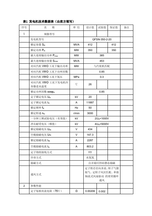
东电350MW发电机技术数据表
kW
652.22
通风损耗
kW
含于以上各项中
杂散损耗
kW
轴承摩擦损耗
kW
电刷摩擦损耗
kW
总损耗ΣQ
kW
3492.57
满载效率η
%
99.01
≥99
5
绝缘等级和温度
定子绕组绝缘等级
F
按B级考核温升
定子绕组THA工况下绕组出水温度
℃
≤85
定子绕组T-MCR工况下绕组出水温度
℃
45~50
定子绕组VWO工况下绕组出水温度
℃
≤70
密封瓦油量
L/min
2×92.5
氢侧
L/min
单流环,合二为一
空侧
L/min
密封瓦温度
℃
≤90
≤90
油冷却器冷却水量
T/h
无
油冷却器冷却水流动阻力
MPa
无
7
主要尺寸和电磁负荷
定子铁芯内径Di
mm
1270
定子铁芯外径Da
mm
2550
定子铁芯长度Li
mm
5100
气隙(单边)g
mm
75
定子外壳压力
Ω
0.00206
0.00204
转子绕组直流电阻(75℃)
Ω
0.1750
0.1731
定子每相对地电容
A
pf
232900
B
pf
232900
C
pf
232900
转子绕组自感
H
1.3681
直轴同步电抗Xd
%
215.14
207.97
横轴同步电抗Xq
12jsdx240ta英文参数

12jsdx240ta英文参数12jsdx240ta English ParametersIn this document, we will outline the 12jsdx240ta parameters in English for easy reference and understanding.1. Parameter 1: Input Voltage- The input voltage for the 12jsdx240ta device should be between 100V to 240V AC.2. Parameter 2: Output Power- The output power of the 12jsdx240ta device is 240 watts.3. Parameter 3: Efficiency- The efficiency of the 12jsdx240ta device is rated at 90%.4. Parameter 4: Operating Temperature- The operating temperature range for the 12jsdx240ta device is -10°C to 40°C.5. Parameter 5: Protection- The 12jsdx240ta device is equipped with over-currentand over-voltage protection.6. Parameter 6: Dimensions- The dimensions of the 12jsdx240ta device are 150mm x100mm x 50mm.7. Parameter 7: Weight- The weight of the 12jsdx240ta device is 1.5kg.8. Parameter 8: Certification- The 12jsdx240ta device is certified to meet CE and RoHS standards.9. Parameter 9: Warranty- The 12jsdx240ta device comes with a 2-year warrantyfrom the date of purchase.10. Parameter 10: Input Connector- The input connector for the 12jsdx240ta device is a standard IEC C14 plug.11. Parameter 11: Output Connector- The output connector for the 12jsdx240ta device is a DC barrel plug with a 5.5mm outer diameter and a 2.1mm inner diameter.12. Parameter 12: Safety- The 12jsdx240ta device is designed with safety in mind and meets all relevant safety standards.In conclusion, the 12jsdx240ta device is a reliable and efficient power supply with a range of features to meet your needs. If you require any additional information, pleaserefer to the user manual or contact our customer support team.。
- 1、下载文档前请自行甄别文档内容的完整性,平台不提供额外的编辑、内容补充、找答案等附加服务。
- 2、"仅部分预览"的文档,不可在线预览部分如存在完整性等问题,可反馈申请退款(可完整预览的文档不适用该条件!)。
- 3、如文档侵犯您的权益,请联系客服反馈,我们会尽快为您处理(人工客服工作时间:9:00-18:30)。
High Frequency, Solid Aluminum TopType 350’s solid aluminum top assures extremely low impedance. With a typical 4 to 6 nH ESL, the self reso-nant frequency is well above 100 kHz. The very low ESR assures the low impedance rating. The capacitors are fitted with three rugged welded mounting leads to provide maximum resistanceHighlightsOperates to beyond 200 kHz Less than 10 nH ESL Solid aluminum top•••SpecificationsCapacitance Range:Voltage Range:Capacitance Tolerance:Operating Temperature Range:Shelf Life:Leakage Current:Cold Impedance:Ripple Current Multipliers:Load Life:Shelf Life:Vibration:90 to 11,000 F 6.3 to 100 Vdc –10 +75%–55 ºC to +105 ºC 500 hours @ +105 ºC ≤0.5 √CV µA at +25 ºC–55 º multiple of +25 ºC Z ≤6 for 6.3 V, 3 for 10 to 50 V, 2 for 75 & 100 V45 ºC 55 ºC 65 ºC 75 ºC 85 ºC 95 ºC 105 ºC 1.661.521.371.201.000.750.36Ambient TemperatureFrequency60 Hz120 Hz 360 Hz 1 kHz 5 kHz 10 kHz & up 6.3 to 20 V 0.530.650.730.900.95 1.0025 to 35 V 0.450.550.650.850.92 1.0050 to 75 V0.360.500.600.800.90 1.00100 V0.290.400.520.750.871.004,000 h @ +105 ºC at full load ∆ Capacitance ±10% ESR 150% of limit DCL 100% of limit500 h @ 105 ºC, capacitance, ESR and DCL, initial requirement10 to 55 Hz, 0.06” and 10 g max, 2 h in each planeOutline DrawingL.025±.015S1 S2DT ±.015Complies with the EU Directive 2002/95/EC requirementrestricting the use of Lead (Pb), Mercury (Hg), Cadmium (Cd), Hexavalent chromium (Cr(VI)), PolyBrominated Biphenyls (PBB) and PolyBrominated Diphenyl Ethers (PBDE).Case DimensionsPart Numbering System350JP 1152U 6R3 C Type Case Code Capacitance Tolerance Voltage Insulation 350See table900 = 90 µF U = –10 +75%6R3 = 6.3 Vdc O = Bare can161 = 160 µF T = –10 +50%063 = 63 Vdc B = Plastic insulation with epoxy 882 = 8800 µF 100 = 100 VdcC = Plastic insulation, no epoxy1152 = 11500 µFCase InchesCode Nominal Insulated S1S2TD x L D x L ±0.015±0.015GE 3/4 x 1 1/8 0.775 x 1.157 0.20.100.3GJ 3/4 x 1 5/8 0.775 x 1.657 0.20.100.3GL 3/4 x 2 1/8 0.775 x 2.157 0.20.100.3GP 3/4 x 2 5/8 0.775 x 2.657 0.20.100.3HE 7/8 x 1 1/8 0.900 x 1.157 0.30.150.4HJ 7/8 x 1 5/8 0.900 x 1.657 0.30.150.4HL 7/8 x 2 1/8 0.900 x 2.157 0.30.150.4HP 7/8 x 2 5/8 0.900 x 2.657 0.30.150.4JJ1 x 1 5/81.025 x 1.6570.30.150.4Typical Performance CurvesType 350 Impedance vs. FrequencyI m p e d a n c e (Ω)Frequency (Hz)10010k 100k 10001M 10M0.0010.010.11.0103,400 µF 6.3 Vdc6,100 µF 6.3 Vdc11,500 µF 6.3 VdcType 350 Operating Life in Kilohours vs. Ripple Current00.10.20.30.40.50.60.70.80.911Rated Ripple-Current MultipleE x p e d t e d O p e r a t i n g L i f e , k h105 ºC95 ºC85 ºC75 ºC 65 ºC 55 ºC45 ºC 1.1 1.2 1.3 1.4 1.5101001000Typical Performance CurvesRatingsESR Max ΩImped.Ripple Nom Cap Catalog +25 ºC Ω +25 ºC A +85 ºC Size (in)(µF)Part Number 120 Hz 20 kHz 100 kHz 20 kHz DxL 6.3 Vdc (8.5 Vdc Surge)1600350GE162U6R3C 0.0870.0430.040 3.23/4 x 1 1/8 2400350HE242U6R3C 0.0650.0350.034 3.77/8 x 1 1/8 3000350GJ302U6R3C 0.0500.0250.025 4.63/4 x 1 5/8 3400350JE342U6R3C 0.0580.0310.031 4.0 1 x 1 1/8 4200350GL422U6R3C 0.0350.0180.019 6.63/4 x 2 1/8 4400350HJ442U6R3C 0.0370.0200.022 5.67/8 x 1 5/8 5400350GP542U6R3C 0.0290.0150.0178.03/4 x 2 5/8 6100350JJ612U6R3C 0.0330.0180.020 6.2 1 x 1 5/8 6300350HL632U6R3C 0.0270.0150.0187.57/8 x 2 1/8 8300350HP832U6R3C 0.0220.0130.0168.87/8 x 2 5/8 8800350JL882U6R3C 0.0240.0140.0168.1 1 x 2 1/8 11000350JP113U6R3C 0.0200.0120.0159.6 1 x 2 5/8 7.5 Vdc (10 Vdc Surge)1500 350GE152U7R5C 0.0910.0440.040 3.23/4 x 1 1/8 2300350HE232U7R5C 0.0680.0350.034 3.77/8 x 1 1/8 2700350GJ272U7R5C 0.0520.0260.025 4.63/4 x 1 5/8 3200350JE322U7R5C 0.0590.0310.030 3.9 1 x 1 1/8 3900350GL392U7R5C 0.0370.0180.019 6.63/4 x 2 1/8 4200350HJ422U7R5C 0.0390.0210.022 5.67/8 x 1 5/8 5100350GP512U7R5C 0.0300.0150.0167.93/4 x 2 5/8 5800350JJ582U7R5C 0.0340.0180.019 6.1 1 x 1 5/8 6000350HL602U7R5C 0.0280.0150.0187.47/8 x 2 1/8 7900350HP792U7R5C 0.0230.0130.0168.87/8 x 2 5/8 8400350JL842U7R3C 0.0250.0140.0168.0 1 x 2 1/8 11000350JP113U7R5C0.0200.0120.0149.51 x2 5/810 Vdc (12 Vdc Surge)1400350GE142U010C 0.0980.0450.040 3.13/4 x 1 1/8 2100350HE212U010C 0.0720.0350.034 3.67/8 x 1 1/8 2600350GJ262U010C 0.0550.0260.025 4.53/4 x 1 5/8 3000350JE302U010C 0.0620.0320.030 3.6 1 x 1 1/8 3800350GL382U010C 0.0390.0190.019 6.53/4 x 2 1/8 3900350HJ392U010C 0.0410.0210.022 5.57/8 x 1 5/8 4800350GP482U010C 0.0310.0150.0167.83/4 x 2 5/8 5400350JJ542U010C0.0360.0190.0205.71 x 1 5/8ESR Max ΩImped.Ripple Nom Cap Catalog +25 ºC Ω +25 ºC A +85 ºC Size (in)(µF)Part Number 120 Hz 20 kHz 100 kHz 20 kHz DxL 10 Vdc (12 Vdc Surge)5600350HL562U010C 0.0300.0150.0187.37/8 x 2 1/8 7300350HP732U010C 0.0240.0130.0168.77/8 x 2 5/8 7800350JL782U010C 0.0260.0140.0167.5 1 x 2 1/8 10000350JP103U010C0.0210.0120.0159.0 1 x 2 5/8 12 Vdc (18 Vdc Surge)1100350GE112U012C 0.1080.0460.042 3.13/4 x 1 1/8 1700350HE172U012C 0.0790.0360.034 3.67/8 x 1 1/8 2000350GJ202U012C 0.0610.0270.025 4.43/4 x 1 5/8 2400350JE242U012C 0.0670.0320.031 3.8 1 x 1 1/8 2900350GL292U012C 0.0440.0190.020 6.43/4 x 2 1/8 3000350HJ302U012C 0.0450.0210.022 5.47/8 x 1 5/8 3700350GP372U012C 0.0350.0160.0177.73/4 x 2 5/8 4200350JJ422U012C 0.0380.0290.020 6.0 1 x 1 5/8 4400350HL442U012C 0.0320.0160.0187.27/8 x 2 1/8 5800350HP582U012C 0.0260.0130.0168.67/8 x 2 5/8 6100350JL612U012C 0.0280.0140.0167.8 1 x 2 1/8 8000350JP802U012C0.0230.0120.0159.3 1 x 2 5/8 16 Vdc (20 Vdc Surge)950350GE951U016C 0.1160.0470.042 3.03/4 x 1 1/8 1500350HE152U016C 0.0850.0370.035 3.57/8 x 1 1/8 1700350GJ172U016C 0.0660.0270.025 4.33/4 x 1 5/8 2000350JE202U016C 0.0710.0330.031 3.7 1 x 1 1/8 2500350GL252U016C 0.0470.0200.020 6.33/4 x 2 1/8 2600350HJ262U016C 0.0480.0220.022 5.37/8 x 1 5/8 3200350GP322U016C 0.0370.0160.0177.63/4 x 2 5/8 3600350JJ362U016C 0.0410.0190.020 5.9 1 x 1 5/8 3800350HL382U016C 0.0340.0160.0187.17/8 x 2 1/8 4900350HP492U016C 0.0280.0130.0168.47/8 x 2 5/8 5200350JL522U016C 0.0290.0140.0167.7 1 x 2 1/8 6800350JP682U016C0.0240.0120.0159.2 1 x 2 5/8 20 Vdc (25 Vdc Surge)800350GE801U020C 0.1250.0480.042 3.03/4 x 1 1/8 1200350HE122U020C 0.0890.0380.035 3.57/8 x 1 1/8 1500350GJ152U020C 0.0700.0280.026 4.23/4 x 1 5/8 1700350JE172U020C0.0750.0330.0313.71 x 1 1/8ESR vs. Temperature Characteristics (10 kHz)-55-40-20025406085105Temperature (ºC)0.1110100Capacitance vs. Temperature (120 Hz)-55-40-20025406085105708090100110≥ 50 Vdc ≤ 40 Vdc E S R - R a t i o t o 25 ºC V a l u eC a p a c i t a n c e - % o f 25 ºC V a l u eTemperature (ºC)≥ 75 Vdc6.3 VdcESR Max ΩImped.Ripple Nom Cap Catalog +25 ºC Ω +25 ºC A +85 ºC Size (in) (µF)Part Number120 Hz20 kHz100 kHz20 kHz DxL20 Vdc (25 Vdc Surge)2100350GL212U020C 0.0500.0200.020 6.23/4 x 2 1/8 2200350HJ222U020C 0.0510.0220.022 5.37/8 x 1 5/8 2800350GP282U020C 0.0400.0170.0177.53/4 x 2 5/8 3000350JJ302U020C 0.0430.0200.020 5.8 1 x 1 5/8 3200350HL322U020C 0.0360.0160.0187.07/8 x 2 1/8 4200350HP422U020C 0.0290.0140.0168.37/8 x 2 5/8 4500350JL452U020C 0.0310.0140.0167.6 1 x 2 1/8 5900350JP592U020C 0.0250.0120.0159.1 1 x 2 5/825 Vdc (30 Vdc Surge)600350GE601U025C 0.1400.0500.042 2.93/4 x 1 1/8 900350HE901U025C 0.1000.0390.035 3.47/8 x 1 1/8 1100350GJ112U025C 0.0790.0290.026 4.13/4 x 1 5/8 1300350JE132U025C 0.0820.0340.031 3.6 1 x 1 1/8 1500350GL152U025C 0.0560.0210.020 6.03/4 x 2 1/8 1600350HJ162U025C 0.0570.0230.022 5.17/8 x 1 5/8 2000350GP202U025C 0.0440.0170.0177.33/4 x 2 5/8 2300350HL232U025C 0.0400.0170.018 6.87/8 x 2 1/8 2300350JJ232U025C 0.0470.0200.021 5.6 1 x 1 5/8 3100350HP312U025C 0.0320.0140.0168.27/8 x 2 5/8 3300350JL332U025C 0.0340.0150.01774.0 1 x 2 1/8 4300350JP432U025C 0.0270.0130.0168.9 1 x 2 5/830 Vdc (40 Vdc Surge)450350GE451U030C 0.1550.0520.043 2.83/4 x 1 1/8 700350HE701U030C 0.1100.0410.035 3.37/8 x 1 1/8 800350GJ801U030C 0.0880.0300.026 4.03/4 x 1 5/8 950350JE951U030C 0.0890.0360.032 3.4 1 x 1 1/8 1100350GL112U030C 0.0620.0220.02 5.83/4 x 2 1/8 1200350HJ122U030C 0.0620.0240.023 5.07/8 x 1 5/8 1500350GP152U030C 0.0480.0180.0177.13/4 x 2 5/8 1700350JJ172U030C 0.0500.0210.021 5.5 1 x 1 5/8 1800350HL182U030C 0.0440.0170.018 6.67/8 x 2 1/8 2300350HP232U030C 0.0350.0150.0168.07/8 x 2 5/8 2500350JL252U030C 0.0360.0160.0177.2 1 x 2 1/8 3200350JP322U030C 0.0290.0130.0168.6 1 x 2 5/840 Vdc (50 Vdc Surge)320350GE321U040C 0.1760.0540.043 2.73/4 x 1 1/8 500350HE501U040C 0.1230.0420.035 3.27/8 x 1 1/8 600350GJ601U040C 0.1000.0310.026 3.93/4 x 1 5/8 700350JE701U040C 0.0990.0370.032 3.4 1 x 1 1/8 850350GL851U040C 0.0700.0230.02 5.73/4 x 2 1/8 900350HJ901U040C 0.0700.0250.023 4.97/8 x 1 5/8 1100350GP112U040C 0.0550.0180.017 6.93/4 x 2 5/8 1200350JJ122U040C 0.0560.0220.021 5.4 1 x 1 5/8 1300350HL132U040C 0.0490.0180.018 6.57/8 x 2 1/8 1700350HP172U040C 0.0390.0150.0167.97/8 x 2 5/8 1800350JL182U040C 0.0400.0160.0177.1 1 x 2 1/8 2300350JP232U040C 0.0320.0130.0168.51 x2 5/8 Ratings。