PSRR测试文档
OPA188运算放大器说明书
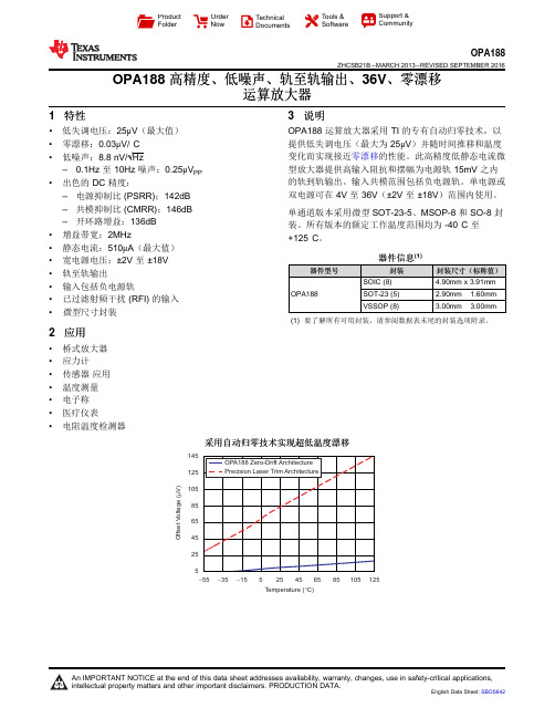
145125105856545255O f f s e t V o l t a g e (V )m -55-15525125Temperature (C)°-35456585105ProductFolder Order NowTechnical Documents Tools &SoftwareSupport &CommunityOPA188ZHCSB21B –MARCH 2013–REVISED SEPTEMBER 2016OPA188高精度、低噪声、轨至轨输出、36V 、零漂移运算放大器1特性•低失调电压:25μV (最大值)•零漂移:0.03μV/°C •低噪声:8.8nV/√Hz–0.1Hz 至10Hz 噪声:0.25μV PP •出色的DC 精度:–电源抑制比(PSRR);142dB –共模抑制比(CMRR):146dB –开环路增益:136dB •增益带宽:2MHz•静态电流:510μA (最大值)•宽电源电压:±2V 至±18V •轨至轨输出•输入包括负电源轨•已过滤射频干扰(RFI)的输入•微型尺寸封装2应用•桥式放大器•应力计•传感器应用•温度测量•电子称•医疗仪表•电阻温度检测器3说明OPA188运算放大器采用TI 的专有自动归零技术,以提供低失调电压(最大为25μV )并随时间推移和温度变化而实现接近零漂移的性能。
此高精度低静态电流微型放大器提供高输入阻抗和摆幅为电源轨15mV 之内的轨到轨输出。
输入共模范围包括负电源轨。
单电源或双电源可在4V 至36V (±2V 至±18V )范围内使用。
单通道版本采用微型SOT-23-5、MSOP-8和SO-8封装。
所有版本的额定工作温度范围均为-40°C 至+125°C 。
器件信息(1)器件型号封装封装尺寸(标称值)OPA188SOIC (8) 4.90mm x 3.91mm SOT-23(5) 2.90mm ×1.60mm VSSOP (8)3.00mm ×3.00mm(1)要了解所有可用封装,请参阅数据表末尾的封装选项附录。
软件自测报告模板

√
5.1.5.2
产品说明应提供该产品中最终用户可调用的功能的概述。
符合要求
√
5.1.5.3
产品说明应描述用户可能遭遇关键缺陷的所有功能。
符合要求
√
5.1.5.4
产品说明应给出用户可能碰到的所有已知的限制。
符合要求
√
5.1.5.5
当有软件组件的选项和版本时,应无歧义地予以指明。
符合要求
√
5.1.5.6
符合要求
√
5.2.3.4
用户文档集应标识该软件能完成的预期工作任务和服务。
符合要求
√
5.2.4
完备性
5.2.4.1
用户文档集应包含使用该软件必需的信息。
符合要求
√
5.2.4.2
用户文档集应说明在产品说明中陈述的所有功能以及最终用户能调用的所有功能。
符合要求
√
5.2.4.3
用户文档集应列出已处理处置、会引起应用系统失效或终止的差错和缺陷,特别是列出那些最终导致数据丢失的应用系统终止的情况。
——
√
5.1.11
产品质量——维护性
5.1.11.1
适用时,产品说明应根据GB/T 25000.10-2016包含有关维护性的陈述,要考虑模块化、可重用性、易分析性、易修改性、易测试性以及维护性的依从性,并以书面形式展示可验证的依从性证据。
——
√
5.1.11.2
产品说明应包括用户所需的维护信息。
——
符合要求
√
5.1.9.3
产品说明应包括关于数据保存和恢复规程的信息。
符合要求
√
5.1.10
产品质量——信息安全性
适用时,产品说明应根据GB/T 25000.10-2016包含有关信息安全性的陈述,要考虑保密性、完整性、抗抵赖性、可核查性、真实性以及信息安全性的依从性,并以书面形式展示可验证的依从性证据。
ASP环境的测试 Microsoft Word 文档
ASP环境的测试把IIS和数据库安装好了之后,就是要对IIS进行配置,配置后即可发布ASP网站。
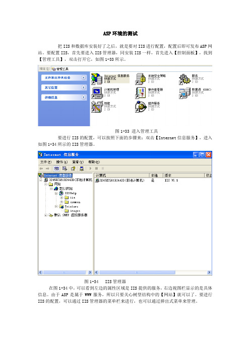
要配置IIS,首先要进入IIS管理器,同安装IIS一样,首先进入【控制面板】,找到【管理工具】,双击打开它,如图1-33所示。
图1-33 进入管理工具要进行IIS的配置,可以按照下面的步骤来:双击【Internet信息服务】,进入如图1-34所示的IIS管理器。
图1-34 IIS管理器在图1-34中,可以看到左边的属性区域是IIS提供的服务,右边视图栏显示的是具体信息。
由于ASP是属于WWW服务,所以只要关心树型结构中的【网站】就可以了。
要进行IIS 的配置,可以通过IIS管理器的菜单栏来进行,也可以通过弹出式菜单来管理。
注意:在IIS提供服务的时候,首先要启动网站服务,则要选中【默认网站】,然后通过工具栏上面的黑色三角形按钮来启动该服务。
启动后,黑色三角按钮失效,此时可以通过“■”按钮来停止服务或者通过“‖”按钮暂停服务。
我们在“默认网站”上单击右键,选择属性选项。
这样就弹出了如图1-35所示的属性对话框。
在属性设置对话框中,可以看到很多属性页,如【网站】、【ISAPI筛选器】、【主目录】、【目录】、【文档】、【目录安全性】、【HTTP头】、【自定义错误】,下面介绍其中重要的属性页。
图1-35 属性页在网站属性页中,最主要的设置是TCP端口的设定。
对于WWW协议而言,默认端口是80。
通常,我们在访问为80端口的Web服务器的时候,只需要输入IP地址或者域名即可。
例如访问“/”。
而如果对方设置的是8080端口的话,则必须采用“:8080”。
这里我们不需要设置任何东西,默认即可。
接下来就是要学习主目录属性页的内容,在图1-35中,选择主目录就进入了,如图1-36所示。
在主目录属性页中,最主要是树型是本地路径的位置,通过改变主目录,可以让网络服务器对应不同的网站内容。
如果主目录设置成“D:\asp”,另外一个路径设置为“E:\Script”。
血氧饱和度

SpO Pulse Ox Wrist Oximeter Reference DesignTI Reference DesignsTI Reference Designs are mixed-signal solutions created by TI’s experts. Verified Desi gns offer the theory, complete PCB schematic & layout, bill of materials and measured performance of the overall system.Circuit DescriptionPulse oximeters measure arterial blood oxygen saturation by sensing absorption properties of deoxygenated and oxygenated hemoglobin using various wavelengths of light. A basic meter is comprised of a sensing probe attached to a patient's earlobe, toe, finger or other body locations, depending upon the sensing method (reflection or transmission), and a data acquisition system for the calculation and eventually display of oxygen saturation level, heart rate and/or blood flow.This reference design discusses the methodology for achieving a Low Power, Portable Pulse Oximeter.High Performance is achieved by using the AFE4400, a Fully Integrated Analog Front End that consists of a low noise receiver channel with an integrated Analog to Digital Converter, an LED transmit section, diagnostics for sensor and LED fault detection. Additional components are an ultra-low power microcontroller (MCU) for calculating the oxygen saturation, a wireless module based on Bluetooth Low Energy (BLE) for exchanging information with smart phones, tablets or PCs, a motion sensor for monitoring the user’s activity, a sensing probe, ferroelectric RAM (FRAM) for data logging, a lithium-polymer rechargeable battery, a battery charger and a battery fuel gauge.Sensing ProbeBluetooth Low Energy ModuleIn general, Pulse Oximeters require ultra-low power consumption and low noise power rails in order to support extended battery life and precision measurements. TI's buck-boost converters provide support for Li-ion battery technologies and 96% efficiency. For additional low noise power rails, high PSRR LDOs are also available. Requirements for wall-plug and USB-port charging can be addressed with the TI's linear lithium low single-cell charger family. Innovative next-generation gas gauge solutions are offered with "Impedance Track" to automatically learn/detect battery characteristics, extending both battery life and system run time.Design ResourcesDesign Archive (ZIP File) All design filesAFE4400SPO2EVM GUI Product FolderAFE4400Product Folder1.Design SummaryThis design takes a block level approach for designing a low power finger based pulse oximeter.1.1Design GoalProvide a SpO Pulse Ox Wrist Oximeter reference example.2. Theory of Operation2.1 Background on PPG MeasurementsPulse oximetry is based on spectrophotometric measurements of changes in blood color. Oxygenated blood is distinctively red, whereas deoxygenated blood has a characteristic dark blue coloration. The optical property of blood in the visible (i.e. between 400 and 700nm) and near-infrared (i.e. between 700 and 1000nm) spectral regions depends strongly on the amount of O2 carried by blood.The method exploits the fact that Hb has a higher optical absorption coefficient in the red region of the spectrum around 660nm compared with HbO2, as illustrated in Figure 1. On the other hand, in the near-infrared region of the spectrum around 940nm, the optical absorption by Hb is lower compared to HbO2.At the isobestic wavelength (i.e. 805nm), where the two curves cross over, the absorbance of light is independent of oxygenation level.Figure 1 Oxygenated versus de-oxygenated blood light absorption of IR and REDThe absorbance of light at a specific wavelength by a homogenous solution can be accurately determined by the Beer-Lambert’s law, using the following equationwhere is the transmitted light intensity, is the incident light intensity, is the specific absorption coefficient of the sample, is the concentration of the sample, and is the path length of light transmission.In oximetry, it is assumed that a hemolyzed blood sample consists of a two-component homogeneous mixture of Hb and HbO2 and that light absorbance by the mixture of these components is additive. However, other variables in the biological media such as bone, skin, tissue, muscle and blood also scatter light.The absorption of light also depends on both skin thickness and color. Therefore, Beer-Lambert’s Law is unable to account for all of these variables.Modern pulse oximetry relies on the detection of a photoplethysmographic (PPG) signal produced by variations in the quantity of arterial blood associated with periodic contractions and relaxations of the heart.As shown in Figure 2, the magnitude of the PPG signal depends on the amount of blood ejected from the heart with each systolic cycle, the optical absorption of blood, absorption by skin and various tissue components, and the specific wavelengths used to illuminate the vascular tissue bed.During systole, when the arterial pulsation is at its peak, the volume of blood in tissue increases. This additional blood absorbs more light, thus reducing the light intensity which is either transmitted or backscattered.During diastole, less blood is present in the vascular bed, thus increasing the amount of light transmitted or backscattered. The pulsatile part of the PPG signal is considered as the “AC” component, and the non- pulsatile part, resulting mainly from the venous blood, skin and tissue, is referred to as the “DC” component. A deviation in the LED brightness or detector sensitivity can change the intensity of the light detected by the sensor. This dependence on transmitted or backscattered light intensity can be compensated by using a normalization technique where the AC component is divided by the DC component, as given in the equation below:(⁄)Thus, the time invariant absorbance due to venous blood or surrounding tissues does not have any effect on the measurement. This normalization is carried out for both the red (R) and the infrared (IR) wavelengths, as shown in Figure 3. The normalized R/IR “ratio of ratios” can then be related empirically to SpO2, as shown in Figure 4. When the ratio is 1, the SpO2 value is about 85%.Figure 2 Variations in light attenuation by tissue illustrating the rhythmic effect of arterial pulsationFigure 3 Normalization of R and IR wavelengths to remove the effects of variation in the incident light intensity or detector sensitivityMost pulse oximeters measure absorbance at two different wavelengths and are calibrated using data collected from CO-oximeters by empirically looking up a value for SpO2, giving an estimation of SaO2 using the empirical relationship given by the equationwhere is based on a normalization where the pulsatile (AC) component is divided by the corresponding non-pulsatile (DC) component for each wavelength, and and are linear regression coefficients which are related to the specific absorptions coefficients of Hb and HbO2.The constants and are derived empirically during in-vivo calibration by correlating the ratio calculated by the pulse oximeter against SaO2 from arterial blood samples by an in vitro oximeter for a large group of subjects. Pulse oximeters read the SaO2 of the blood accurately enough for clinical use under normal circumstances because they use a calibration curve based on empirical data shown in figure 4.Figure 4 Empirical relationship between arterial SaO2 and normalized (R/IR) ratio2.2 Hardware overview and circuit descriptionThe key components required for acquiring and signal-conditioning the PPG signals are the LED, photodetector and AFE. Some commercially available AFEs, like TI’s AFE4400,integrate both the LED driver circuitry and the photodiode signal conditioning circuitry in a single package, Figure 5. This new generation of AFEs can drive the LED currents in using an H-bridge configuration capable of driving up to 150 mA/leg, with short-circuit protection. They can also increase the dynamic range greater than 105 dB and create a current reference independent of the IR and red LEDs.Figure 5 Commercially available AFEs like TI’s AFE4400 integrate the LED driver circuitry and the photodiode signal conditioning circuitry in a single packageThe photodiode circuitry embedded into these devices can amplify currents below 1 µA with 13 bits of resolution. It is ultra-low-power (<4 mW) and has a programmable TIA. The AFE consumes less than 3 mA of current when active.2.2.1 LED Transmit SectionAs highlighted in Figure 6, the transmit stage contains two sections: the LED driver and LED current control section.a.LED Driver - There are two LEDs, one for the visible red wavelength and another for the infrared wave length. To turnthem on, an H-Bridge circuit is used. The LED1_ON and LED2_ON signal decide which LED to turn on (the whole circuit is time multiplexed).b.LED Current Control– The current source () locally regulates and ensures that the actual LED current tracks thespecified reference. The LED1 and LED2 reference current can be independently set by Register. The 8-bit current resolution here meets a dynamic range of better than 105dB (based on a 1-sigma LED current noise).c. A Push-Pull LED driver is also supported, please refer to AFE4400 Datasheet for detail.Figure 6 LED Transmit Section2.2.2 Receiver Stage2.2.2.1 I-V Amplifier (Transimpedance Amplifier) and Ambient Cancellation SectionV TIAOUTFigure 7 Receiver Section – Stage 1The RX Stage consists of a differential current-to –voltage transimpedance amplifier that converts the input photodiode current into a appropriated voltage, as shown in Figure 5. The feedback resistor of the amplifier () is programmable to support a wide range of photodiodes currents. (Available values in AFE4400: 1MΩ, 500kΩ, 250kΩ, 100kΩ, 50kΩ, 25kΩ, and 10kΩ)The differential voltage at the TIA output includes the pleth component (the desired signal) and a component resulting from the ambient light leakage:The feedback resistor and feedback capacitor form a low-pass filter for the input signal current. Always ensure that the low-pass filter has sufficiently high bandwidth (as shown by Equation below) because the input current consists of pulses. For this reason, the feedback capacitor is also programmable. (Available value include: 5pF, 10pF, 25pF, 50pF, 100pF and 250pF. Any combination of these capacitors can also be used)The TIA is followed by the second stage, which consists of a current digital-to-analog converter (DAC) that sources the cancellation current and an amplifier that gains up the pleth component alone. The current DAC () has a cancellation current range of 10 uA with 10 steps (1 uA each). The amplifier has five programmable gain settings (): 1, 1.414, 2, 2.828 and 4.The receiver provides digital samples corresponding to ambient duration. The host processor can use these ambient values to estimate the amount of ambient light leakage. The processor must then set the value of the ambient cancellation DAC. Using the set value, the ambient cancellation stage subtracts the ambient component and gains up only the pleth component of the received signal.The differential output of the second stage is :[ ]Where:= 100kΩ,= photodiode current pleth component,= photodiode current ambient component, and= the cancellation current DAC value (as estimated by the host processor).2.2.2.2Filter and Analog-to-Digital ConverterFigure 8 Receiver Section – Stage 2The output of the ambient cancellation amplifier is separated into LED2 and LED1 channels.1)When LED2 is on, the amplifier output is filtered and sampled on capacitor ,2)When LED1 is on, the amplifier output is filtered and sampled on capacitor ,3)In between the LED2 and LED1 pulses, the idle amplifier output is sampled to estimate the ambient signal oncapacitors and .The sampling duration is termed the Rx sample time and is programmable for each signal, independently. The sampling can start after the I-V amplifier output is stable (to account for LED and cable settling times). The Rx sample time is used for all dynamic range calculations; the minimum time supported is 50µs.A single, 22-bit ADC converts the sampled LED2, LED1, and ambient signals sequentially. Each conversion takes 25% of the pulse repetition period and provides a single digital code at the ADC output. Note that four data streams are available at the ADC output (LED2, LED1, ambient LED2, and ambient LED1) at the same rate as the pulse repetition frequency. The ADC is followed by a digital ambient subtraction block that additionally outputs the (LED2–ambientLED2) and (LED1–ambient LED1) data values.2.2.2.3DiagnosticsThe device includes diagnostics to detect open or short conditions of the LED and photo sensor, LED current profile feedback, and cable on or off detection. By default, the diagnostic function takes tDIAG = 8 ms to complete after the DIAG_EN register bit is enabled. The diagnostics module, when enabled, checks for nine types of faults sequentially. The faults are listed below: 2.2.2.4Photodiode-Side Fault DetectionFigure 9 shows the diagnostic for the photodiode-side fault detection.Figure 9 Photodiode Side Fault Detection2.2.2.5Transmitter-Side Fault DetectionFigure 10 shows the diagnostic for the photodiode-side fault detection.Figure 10 Transmitter Fault Detection2.3 MicrocontrollerIn this design example, the microcontroller is used to calculate the heart rate, merge the motion sensor data, and process the AFE information. The microcontroller should have specific features including the ability to maintain the context at all times. It should also have a limited power budget because it will be continuously running and nobody wants to drain the batteries.2.4Motion SensorsSensors are a fundamental part of the human machine interface (HMI). They help the system identify the context and environmental conditions. Motion sensors such as accelerometers, gyroscopes, and magnetometers help identify whether a person is seated, walking, or running. They are key elements to identify the orientation of the arm, wrist, or other specific part of the body where the activity monitor is located.They also help to track the travel distances and provide a more accurate position of the system by increasing the resolution of the GPS with dead-reckoning algorithms.2.5Communication LinkThe system described in this article has both wireless and wired communication links. The wireless communication link is based on BLE and is based on the BR-LE4.0-S2A, an FCC-certified (Federal Communications Commission) system-in-PCB (printed-circuit board) module available online that only requires a few external components.This module works with AT-based commands and is easy to use since it includes a network processor that handles all the transactions required by the Bluetooth 4.0 stack. The wired communication is based on USB 2.0. The microcontroller’s built-in module requires only a few external components. USB is also used for charging the lithium-polymer battery.2.6Battery Charger and Fuel GaugeThe battery charger operates from either a USB port or ac adapter and supports charge currents up to 1.5 A. The input voltage range with input overvoltage protection supports unregulated adapters. The USB input current limit accuracy and startup sequence allow the battery charger to meet the USB-IF inrush current specification. Additionally, the input dynamic power management prevents the charger from crashing incorrectly configured USB sources.The battery fuel gauge circuits an easy-to-configure microcontroller peripheral that provides system-side fuel gauging for single-cell lithium-ion batteries. The device requires minimal user configuration and system microcontroller firmware development. The battery fuel gauge uses the impedance track algorithm for fuel gauging and provides information such as remaining battery capacity (mAh), state-of-charge (%), and battery voltage (mV).3. Verification and measured performance 3.1 Health Hub Demonstration SuiteThe figure below shows up the Health Hub measurement setup hardware description. The app requires a PC, a BlueRadios USB Serial Dongle along with the wrist watch data acquisition system and the sensing probe. The pictured device connects to the app via Bluetooth low energy.Figure 11 Health Hub Measurement Setup Hardware Description3.2 Health Hub App 3.2.1 Interface OverviewHealth Hub is designed to allow the control and display of many BLE enabled health monitoring devices on a single screen. The screen is divided into multiple discrete areas, Figure 12, called Device Controls and each area allows a specific BLE enabled health monitoring device control.3.3 Demonstration usage Terminology:Advertising mode : the Bluetooth radio is broadcasting advertising data; this allows another device to initiate a connection to the advertising device.Device : a piece of hardware required for a demo.Device control : The area on the screen of the app that controls a device.BlueRadios USBSerial DongleWrist Watch Data Acquisition SystemFigure 12 Health Hub PC GUI Interface with highlighted Device Controls3.3.1 Common OperationsCommon operations apply to all of the demos with the Health Hub app.3.3.1.1 Find DevicesThe first step in initiating a connection to a Health Hub demonstration device is to have the PC finding the device. To this end, the desired device must be in advertising mode. Generally the devices will advertise any time they are turned on and not connected. When the Pulse Ox is in advertising mode the green LED D7 on the wrist watch will be flashing. To find a device press the Discover Devices button as shown in the figure below. The icon will change to discovering and will find devices for about ten seconds.Figure 13 PC GUI front panel before and after searching for BLE enabled health monitoring devices3.3.1.2 ConnectionThe second step is to form a connection. Before finding a device by using Discover Devices the device controls appear as in the figure below.Figure 14 BLE enabled device not foundAfter a device has been found the device control will appear as in the figure below.Figure 15 Device found – connection can be establishedWhen the Connect button is pressed a selector will be shown as belowFigure 16 Desired Device selection from the listWhen the desired device is selected from the list, the app will form a connection to the device over Bluetooth low energy. After connection the device control will open fully and control over the device can begin. The solid blue LED labeled D8 indicates the connected state. When the device is reporting periodic data, the blue LED labeled D2 will flash. Periodic data only is used with the Wrist Based HRM device control. When the device is reporting graphic data, the green LED labeled D1 will be on. Live Monitor uses both periodic and graphic data.NOTE if after selecting a device from the selector the device control becomes unavailable, an immediate disconnect has occurred. If this happens repeatedly the devices batteries may be depleted.3.4 Measured ResultsThe watch should be attached comfortably around the user’s wrist. The sensor cable should be connected to the micro USB port next to the on/off switch close to the Texas instruments logo. The sensor should be clipped on one of the user’s fingers.Figure 17 Measurement setupThe following figure shows up some measurement resultsIMPORTANT NOTICETexas Instruments Incorporated and its subsidiaries(TI)reserve the right to make corrections,enhancements,improvements and other changes to its semiconductor products and services per JESD46,latest issue,and to discontinue any product or service per JESD48,latest issue.Buyers should obtain the latest relevant information before placing orders and should verify that such information is current and complete.All semiconductor products(also referred to herein as“components”)are sold subject to TI’s terms and conditions of sale supplied at the time of order acknowledgment.TI warrants performance of its components to the specifications applicable at the time of sale,in accordance with the warranty in TI’s terms and conditions of sale of semiconductor products.Testing and other quality control techniques are used to the extent TI deems necessary to support this warranty.Except where mandated by applicable law,testing of all parameters of each component is not necessarily performed.TI assumes no liability for applications assistance or the design of Buyers’products.Buyers are responsible for their products and applications using TI components.To minimize the risks associated with Buyers’products and applications,Buyers should provide adequate design and operating safeguards.TI does not warrant or represent that any license,either express or implied,is granted under any patent right,copyright,mask work right,or other intellectual property right relating to any combination,machine,or process in which TI components or services are rmation published by TI regarding third-party products or services does not constitute a license to use such products or services or a warranty or endorsement e of such information may require a license from a third party under the patents or other intellectual property of the third party,or a license from TI under the patents or other intellectual property of TI.Reproduction of significant portions of TI information in TI data books or data sheets is permissible only if reproduction is without alteration and is accompanied by all associated warranties,conditions,limitations,and notices.TI is not responsible or liable for such altered rmation of third parties may be subject to additional restrictions.Resale of TI components or services with statements different from or beyond the parameters stated by TI for that component or service voids all express and any implied warranties for the associated TI component or service and is an unfair and deceptive business practice. TI is not responsible or liable for any such statements.Buyer acknowledges and agrees that it is solely responsible for compliance with all legal,regulatory and safety-related requirements concerning its products,and any use of TI components in its applications,notwithstanding any applications-related information or support that may be provided by TI.Buyer represents and agrees that it has all the necessary expertise to create and implement safeguards which anticipate dangerous consequences of failures,monitor failures and their consequences,lessen the likelihood of failures that might cause harm and take appropriate remedial actions.Buyer will fully indemnify TI and its representatives against any damages arising out of the use of any TI components in safety-critical applications.In some cases,TI components may be promoted specifically to facilitate safety-related applications.With such components,TI’s goal is to help enable customers to design and create their own end-product solutions that meet applicable functional safety standards and requirements.Nonetheless,such components are subject to these terms.No TI components are authorized for use in FDA Class III(or similar life-critical medical equipment)unless authorized officers of the parties have executed a special agreement specifically governing such use.Only those TI components which TI has specifically designated as military grade or“enhanced plastic”are designed and intended for use in military/aerospace applications or environments.Buyer acknowledges and agrees that any military or aerospace use of TI components which have not been so designated is solely at the Buyer's risk,and that Buyer is solely responsible for compliance with all legal and regulatory requirements in connection with such use.TI has specifically designated certain components as meeting ISO/TS16949requirements,mainly for automotive use.In any case of use of non-designated products,TI will not be responsible for any failure to meet ISO/TS16949.Products ApplicationsAudio /audio Automotive and Transportation /automotiveAmplifiers Communications and Telecom /communicationsData Converters Computers and Peripherals /computersDLP®Products Consumer Electronics /consumer-appsDSP Energy and Lighting /energyClocks and Timers /clocks Industrial /industrialInterface Medical /medicalLogic Security /securityPower Mgmt Space,Avionics and Defense /space-avionics-defense Microcontrollers Video and Imaging /videoRFID OMAP Applications Processors /omap TI E2E Community Wireless Connectivity /wirelessconnectivityMailing Address:Texas Instruments,Post Office Box655303,Dallas,Texas75265Copyright©2013,Texas Instruments Incorporated。
LDO稳压芯片重要测试参数
1 LDO选型关键指标及定义1.1 输入电压范围LDO的输入电压范围决定了最低的可用输入电源电压。
指标可能提供宽的输入电压范围,最小的输入电压VIN必须大于VOUT+VDO。
需要注意,这与器件Datasheet中所给出的输入电压最小值无关。
1.2压差压差指保持电压稳定所需的输入电压和输出电压之间的最小差值。
也就是说,LDO能够在输入电压降低时保持输出负载电压不变,直到输入电压接近输出电压加上压差,在这个点输出电压将“失去”稳定。
压差应尽可能小,以使功耗最小,效率最高。
当输出电压降低到低于标称值 100mV的电压时,通常被认为达到了这个压差。
负载电流和结点温度会影响这个压差。
最大压差值应在整个工作温度范围和负载电流条件下加以规定。
1.3效率在忽略LDO静态电流的情况下,可以采用VOUT/VIN 式子来计算效率。
1.4功耗可以根据公式PD = (VIN - VOUT) * IOUT 计算。
这里PD 与器件封装类型、环境温度(TA)和器件最大结温(TJMAX)密切相关。
如果功率耗散较高,同时又苛求较高的效率,那么应优先考虑选择降压型DC/DC 稳压器。
1.5反向泄漏保护在某些LDO的输出端上的电压高于输入端的电压的特殊应用中,反向泄漏保护可以有效防止电流从LDO的输出端流向输入端。
如果忽视这点,这种反向泄漏会损坏输入电源,特别是当输入电源为电池的时候,尤其需要重视。
1.6接地(静态)电流静态电流Iq就是输入电流Iin和负载电流IOUT之间的差值,在规定的负载电流条件下测量。
对于固定电压稳压器,Iq等于接地电流Ig。
对于可调稳压器,静态电流等于接地电流减去来自外部分压电阻网络中的电流。
1.7关断电流关断电流指设备禁用时LDO消耗的输入电流,对便携LDO来说通常低于1.0 µA。
这个指标对于便携设备关机时长待机期间的电池寿命来说很重要。
1.8输出电压精度ADI公司的LDO具有很高的输出电压精度,在工厂制造时就被精确调整到±1%之内(25℃)。
MCP73871中文文档

18, 19 2 6
CE
IN
IN
IN
OUT
系统 负载
7 STAT2 8 3 STAT1 LBO SEL PROG2 TE CE
单节 锂离子电池
低 低 低 低
高 4 高 高 高 9 17
PROG3
12 RPROG3
VSS 10, 11, EP
DS22090A_CN 第 2 页
2009 Microchip Technology Inc.
2009 MicrochiБайду номын сангаас Technology Inc.
DS22090A_CN 第 1 页
MCP73871
封装类型
MCP73871 20 引脚 QFN VBAT_SENSE 15 VBAT 外露的金属 焊盘 VSS 14 VBAT 13 PROG1 12 PROG3 11 VSS 6 PG 7 STAT2 8 STAT1 / LBO 9 TE 10 VSS
VREG + 0.25V VREG + 0.17V — 4.121 4.221 4.372 4.422 +0.5 +0.75 0.20 0.18 — — 110 1100 100 500
V V mV V V V % % %/V % dB dB mA mA mA mA
VDD=[VREG( 典型值 )+1V] IOUT=10 mA TA=-5°C 至 +55°C TA= +25°C TA= -5°C 至 +55°C VDD=[VREG( 典型值 )+1V] 至 6V IOUT=10 mA IOUT=10 mA 至 150 mA VDD= [VREG( 典型值 )+1V] IOUT=10 mA, 1 kHz IOUT=10 mA, 10 kHz PROG1 = 10 kΩ PROG1 = 1 kΩ, TA=-5°C 至 +55°C, SEL = 高 PROG2 = 低, SEL = 低, (注 2) PROG2 = 高, SEL = 低, (注 2) TA= -5°C 至 +55°C
PSRR非迟滞测试方法

S-89230 系列 S-89240 系列 S-89230 系列 S-89240 系列 S-89230 系列 S-89240 系列 S-89230 系列 S-89240 系列
(除特殊注明以外∶Ta = +25°C) 最小值 典型值 最大值 单位
−
26
−
μs
−
100
−
μs
−
5
−
μs
−
22
−
μs
−
3
−
μs
2. 封装
封装名
SNT-8A TMSOP-8
封装图面 PH008-A-P-SD FM008-A-P-SD
图面号码
卷带图面
带卷图面
PH008-A-C-SD FM008-A-C-SD
PH008-A-R-SD FM008-A-R-SD
焊接图面 PH008-A-L-SD
−
3. 产品名目录
产品名
S-89230BC-I8T1U S-89230BC-K8T2U S-89240BC-I8T1U S-89240BC-K8T2U *1. VDD = 3.0 V 时的值
端子内容
输出端子 1 逆变输入端子 1 非逆变输入端子 1 GND 端子 非逆变输入端子 2 逆变输入端子 2 输出端子 2 正电源端子
4
精工电子有限公司
Rev.3.0_00
微型模拟系列 CMOS 比较器 S-89230/89240 系列
绝对最大值定额
表4
(除特殊注明以外:Ta = +25°C)
−
−
V
3
−
− 0.01 V
4
60
70
−
dB
AD8219中文文档

零漂移单向分流监控器AD8219Rev. AInformation furnished by Analog Devices is believed to be accurate and reliable. However, noresponsibility is assumed by Analog Devices for its use, nor for any infringements of patents or other rights of third parties that may result from its use. Speci cations subject to change without notice. No license is granted by implication or otherwise under any patent or patent rights of Analog Devices. T rademarks and registered trademarks are the property of their respective owners. One Technology Way, P.O. Box 9106, Norwood, MA 02062-9106, U.S.A. Tel: 781.329.4700 Fax: 781.461.3113 ©2011 Analog Devices, Inc. All rights reserved.FUNCTIONAL BLOCK DIAGRAM9415-1Figure 1.特性高共模电压范围工作范围:4 V至80 V耐压范围:-0.3 V至+85 V缓冲输出电压增益 = 60 V/V宽工作温度范围:−40°C至+125°C出色的交流和直流性能失调漂移:±100 nV/°C(典型值)失调:±50 μV(典型值)增益漂移:±5 ppm/°C(典型值)直流共模抑制比(CMRR):110 dB(典型值)应用高端电流检测48 V电信设备电源管理基站单向电机控制精密高压电流源概述AD8219是一款高压、高分辨率分流放大器。