IRLI2203NPBF中文资料
IRFR220NTRPBF中文资料
Units
mJ A mJ
Thermal Resistance
Parameter
RθJC RθJA RθJA Junction-to-Case Junction-to-Ambient (PCB mount)* Junction-to-Ambient Parameter Continuous Source Current (Body Diode) Pulsed Source Current (Body Diode) Diode Forward Voltage Reverse Recovery Time Reverse RecoveryCharge Forward Turn-On Time
RDS(on) , Drain-to-Source On Resistance (Normalized)
I D , Drain-to-Source Current (A)
TJ = 25 ° C
10
3.0 2.5
TJ = 175 ° C
2.0 1.5
1
1.0
0.5 0.0 -60 -40 -20
0.1 4.0
Notes through are on page 10
1
11/29/00
元器件交易网
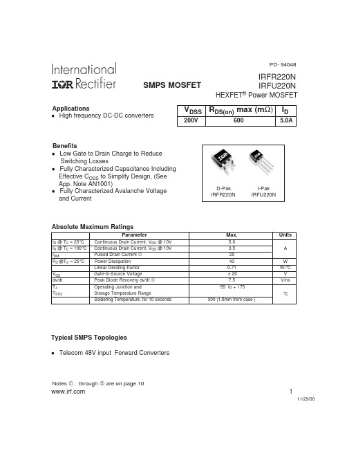
IRFR/U220N
Static @ TJ = 25°C (unless otherwise specified)
Parameter Drain-to-Source Breakdown Voltage ∆V(BR)DSS/∆TJ Breakdown Voltage Temp. Coefficient RDS(on) Static Drain-to-Source On-Resistance VGS(th) Gate Threshold Voltage V(BR)DSS IDSS IGSS Drain-to-Source Leakage Current Gate-to-Source Forward Leakage Gate-to-Source Reverse Leakage Min. Typ. Max. Units Conditions 200 ––– ––– V VGS = 0V, I D = 250µA ––– 0.23 ––– V/°C Reference to 25°C, ID = 1mA ––– ––– 600 mΩ VGS = 10V, I D = 2.9A 2.0 ––– 4.0 V VDS = VGS , ID = 250µA ––– ––– 25 VDS = 200V, VGS = 0V µA ––– ––– 250 VDS = 160V, VGS = 0V, T J = 150°C ––– ––– 100 VGS = 20V nA ––– ––– -100 VGS = -20V
IRS2113-1PBF中文资料

Delay Matching (IRS2110) 10 ns max. (IRS2113) 20 ns max.
Packages
Description
The IRS2110/IRS2113 are high voltage, high speed power MOSFET and IGBT drivers with independent high and low side referenced output channels. Proprietary HVIC and latch immune CMOS technologies enable ruggedized monolithic construction. Logic inputs are compatible with standard CMOS or LSTTL output, down to 3.3 V logic. The output drivers feature a high pulse current buffer stage designed for minimum driver cross-conduction. Propagation delays are matched to simplify use in high frequency applications. The floating channel can be used to drive an N-channel power MOSFET or IGBT in the high side configuration which operates up to 500 V or 600 V.
High side floating supply offset voltage High side floating output voltage Low side fixed supply voltage Low side output voltage Logic supply voltage Logic supply offset voltage Logic input voltage (HIN, LIN, & SD) Allowable offset supply voltage transient (Fig. 2)
IR2233中文资料

3-PHASE BRIDGE DRIVERData Sheet No. PD60107 revU 1Features• dV/dt immune•up to 25V for transient••• Independent 3 half-bridge drivers•• 2.5V logic compatible• Outputs out of phase with inputs • Also available LEAD-FREEDescriptioncurrent buffer stage designed for minimum driver cross-conduction. Propagation delays are matched to simplify use in high frequency applications. The floating channels can be used to drive N-channel power MOSFETs or IGBTs in the up to 600V or 1200VTypical Connection(Refer to L ead Assignments for correct pin configuration). This/These diagram(s) show electrical connections only.Please refer to our Application Notes and DesignTips for proper circuit board layout.Dynamic Electrical CharacteristicsV BIAS (V CC , V BS1,2,3) = 15V, V S1,2,3 = V SS , T A = 25o C and C L = 1000 p F unless otherwise specified.Lead DefinitionsSymbol Lead DescriptionHIN1,2,3L ogic inputs for high side gate driver outputs (HO1,2,3), out of phase.LIN1,2,3L ogic inputs for low side gate driver outputs (LO1,2,3), out of phase.FAULT Indicates over-current or undervoltage lockout (low side) has occurred, negative logic. V CC L ogic and low side fixed supply.ITRIP Input for over-current shut down.FLT-CLR L ogic input for fault clear, negative logic.SD L ogic input for shut down.CAO Output of current amplifier.CA-Negative input of current amplifier.CA+Positive input of current amplifier.V SS L ogic ground.COM L ow side return.V B1,2,3High side floating supplies.HO1,2,3High side gate drive outputs.V S1,2,3High side floating supply returns.LO1,2,3L ow side gate drive outputsITRIP FLT-CLR CAOCA-CA+SDVSS COMLO3LO2LO1VS3HO3VB3FAULTLIN3LIN2LIN1HIN3HIN2HIN1VCCVB1HO1VS1VB2HO2VS2ITRIPFLT-CLRCAOCA-CA+SDVSSCOMLO3LO2LO1VS3HO3VB3FAULTLIN3LIN2LIN1HIN3HIN2HIN1VCCVB1HO1VS1VB2HO2VS228 L ead DIP 44 L ead PLCC w/o 12 L eads 28 L ead SOIC (Wide Body)IR2133 IR2135 IR2233 IR2235IR2133JIR2135JIR2233JIR2235JIR2133SIR2135SIR2233SIR2235S Part NumberFigure 1. Input/Output Timing DiagramSDITRIPHIN1,2,3LIN1,2,3HO1,2,3LO1,2,3FLT-CLRFAULTFigure 2. Switching Time Waveform DefinitionsFigure 3. Deadtime Waveform DefinitionsFigure 4. Overcurrent Shutdown WaveformFigure 4.5 Input Filter FunctionPer SCOP 200-002IR WORLD HEADQUARTERS: 233 Kansas St., El Segundo, California 90245 Tel: (310) 252-7105This product has been qualified per industrial levelData and specifications subject to change without notice. 4/12/2004。
LP2203F180LXBC05中文资料

SPECIFICATIONSElectrical Ratings 100mA @ 30VDC Electrical Life 100,000 cycles typical Contact Resistance < 50 mΩ initial Actuation Force 180 +/- 50gF Actuator Travel 1.5 mm to lock2.5 mm full travel Dielectric Strength 1000Vrms min Insulation Resistance > 100MΩ minOperating Temperature Storage Temperature -40°C to 85°C -40°C to 85°CMATERIALS ←RoHS COMPLIANTActuator AcetalHousing PBTCover Acetal Latching Pin Stainless SteelSpring StainlessSteel Contacts PhosphorBronze, Silver Plated Terminals Brass, Silver Plated ORDERING INFORMATION1. Series:LP2203LP22032. Actuation Force:F180 = 180gFF1803. Latching:N = Non-latchingL = LatchingN4. Actuator Options:X = 2mm X 3mm headY = 3.3 square headZ = 2.8 square headZ A5. Termination:A = PC Pins, straightB = PC pins with bend6. Caps:Blank = No CapC01C02C03C04C05C11C12C13C14C15C16C17C18C19C22C23C24C25Cap Colors:**See Cap Options for color availability**Caps available with Y & Z actuators onlyDIMENSIONSX Y ZSCHEMATIC & PC LAYOUTTERMINATIONA BCAP OPTIONS ←FOR Z ACTUATORC01_1 = White,2 = Black,3 = Red, 9 = Light Gray Contact Factory for other available colors C02_1 = White,2 = Black,3 = Red, 9 = Light Gray Contact Factory for other available colors C03_1 = White,2 = Black,3 = Red, 9 = Light Gray Contact Factory for other available colorsC04_1 = White,2 = Black,3 = Red, 9 = Light Gray Contact Factory for other available colors C05_1 = White,2 = Black,3 = Red, 9 = Light Gray Contact Factory for other available colorsCAP OPTIONS ←FOR Y ACTUATORC11_1 = White,2 = Black,3 = RedContact Factory for other available colorsC12_1 = White,2 = Black,3 = RedContact Factory for other available colorsC13_1 = White,2 = Black,3 = RedContact Factory for other available colorsC14_1 = White,2 = Black,3 = RedContact Factory for other available colorsC15_2 = Black, 0 = ClearContact Factory for other available colorsC16_1 = White,2 = Black,3 = Red, 7 = BlueContact Factory for other available colorsC17_2 = Black, 0 = ClearContact Factory for other available colorsC18_1 = White,2 = Black, 9 = Light GrayContact Factory for other available colorsC19_1 = White,2 = Black,3 = Red, 8 = Dark GrayContact Factory for other available colorsC22_2 = Black, 8 = Dark Gray, 9 = Light GrayContact Factory for other available colorsC23_0 = MetallicContact Factory for other available colorsC24_0 = MetallicContact Factory for other available colorsC25_2 = Black, 8 = Dark Gray, 9 = Light GrayContact Factory for other available colors。
IR2153SPBF;IR2153PBF;IR2153DPBF;IR2153STRPBF;IR2153;中文规格书,Datasheet资料

Features••15.6V zener clamp on Vcc •True micropower start up•Tighter initial deadtime control••••Lower power level-shifting circuit•••Low side output in phase with R T•••ESD protection on all leads •Also available LEAD-FREE(NOTE:For new designs, we recommendIR’s new product IRS2153D)SELF-OSCILLATING HALF-BRIDGE DRIVERProduct SummaryTypical Connections600V MAXIR2153(D)(S) &(PbF)Descriptionporates a high voltage half-bridge gate driver with a front end oscillator similar to the industry standard CMOS 555 timer. The IR2153 provides more functionality and is easier to use than previous ICs. A shutdown feature has been designed into the C T pin, so that both gate driver outputs can be disabled using a low voltage control signal. In addition, the gate driver output pulse widths are the same once the rising undervoltage lockout threshold on V CC has been reached, resulting in a more stable profile of frequency vs time at startup.Noise immunity has been improved significantly, both by lowering the peak di/dt of the gate drivers, and by increasing the undervoltage lockout hysteresis to 1V. Finally, special attention has been payed to maximizing the latch immunity of the device, and providing comprehensive ESD protection on all pins.8 Lead SOIC Data Sheet No. PD60062 revOIR2153(D)(S) & (PbF)NOTE:For new designs, we recommend IR’s new product IRS2153DNote 1:This IC contains a zener clamp structure between the chip V CC and COM which has a nominal breakdown voltage of 15.6V. Please note that this supply pin should not be driven by a DC, low impedance power source greater than the V CLAMP specified in the Electrical Characteristics section.Note 2:Care should be taken to avoid output switching conditions where the V S node flies inductively below ground by more than 5V.Note 3:Enough current should be supplied to the V CC pin of the IC to keep the internal 15.6V zener diode clamping the voltage at this pin.Recommended Operating ConditionsFor proper operation the device should be used within the recommended conditions.Absolute Maximum RatingsAbsolute maximum ratings indicate sustained limits beyond which damage to the device may occur. All voltage param-eters are absolute voltages referenced to COM, all currents are defined positive into any lead. The thermal resistance and power dissipation ratings are measured under board mounted and still air conditions.IR2153(D)(S) & (PbF)NOTE:For new designs, we recommendIR’s new product IRS2153DSymbol ComponentMin.Max.UnitsR T Timing resistor value 10— k ΩC TC T pin capacitor value330—pFRecommended Component ValuesIR2153(D)(S) & (PbF)NOTE:For new designs, we recommend IR’s new product IRS2153DElectrical CharacteristicsV BIAS (V CC , V BS ) = 12V, C L = 1000 pF, C T = 1 nF and T A = 25°C unless otherwise specified. The V IN , V TH and I IN parameters are referenced to COM. The V O and I O parameters are referenced to COM and are applicable to the respective output leads: HO or LO.IR2153(D)(S) & (PbF)NOTE:For new designs, we recommendIR’s new product IRS2153DSymbolDescriptionV CC Logic and internal gate drive supply voltage R T Oscillator timing resistor input C T Oscillator timing capacitor input COM IC power and signal ground LO Low side gate driver outputV S High voltage floating supply return HO High side gate driver outputV BHigh side gate driver floating supplyLead Definitions8 Lead PDIP 8 Lead SOICIR2153DIR2153(S)NOTE: The IR2153D is offered in 8 lead PDIP only.Electrical Characteristics (cont.)IR2153(D)(S) & (PbF)NOTE:For new designs, we recommendIR’s new product IRS2153DFunctional Block Diagram for IR2153(S) Functional Block Diagram for IR2153DIR2153(D)(S) & (PbF)NOTE:For new designs, we recommend IR’s new product IRS2153DFigure 1. Input/Output Timing DiagramFigure 3. Deadtime Waveform DefinitionsR TTCLAMPR T Figure 2. Switching Time Waveform Definitions(HO)(LO)IR2153(D)(S) & (PbF)NOTE:For new designs, we recommendIR’s new product IRS2153DLEADFREE PART MARKING INFORMATIONORDER INFORMATIONBasic Part (Non-Lead Free)8-Lead PDIP IR2153 order IR21538-Lead SOIC IR2153S order IR2153S 8-Lead PDIP IR2153D order IR2153DLeadfree Part8-Lead PDIP IR2153 order IR2153PbF 8-Lead SOIC IR2153S order IR2153SPbF 8-Lead PDIP IR2153D order IR2153DPbFIR WORLD HEADQUARTERS: 233 Kansas St., El Segundo, California 90245 Tel: (310) 252-7105This product has been qualified per industrial levelData and specifications subject to change without notice. 2/8/2006Per SCOP 200-002分销商库存信息:IRIR2153SPBF IR2153PBF IR2153DPBF IR2153STRPBF IR2153IR2153SIR2153STR IR2153D。
三位一体的低压电调节器说明书

Single Pole (One location) or 3-Way (Multi-location)Magnetic Low-Voltage DimmerCat. No. VZM1Ø-1L, 1000VA (Lighted)120VAC, 60HzINSTALLATION INSTRUCTIONSDI-000-VZM10-02CWARNINGS AND CAUTIONS:• To be installed and/or used in accordance with appropriate electrical codes and regulations.• If you are unsure about any part of these instructions, consult a qualified electrician.• To avoid overheating and possible damage to this device and other equipment, do not install to control a receptacle, fluorescent lighting, a motor- or a transformer-operated appliance.• Use with magnetic low-voltage transformers, incandescent, or 120V halogen fixtures only. Use a Leviton electronic low-voltage dimmer to control electronic (solid state) low-voltage transformers.• When magnetic low-voltage circuits are operated at a dim level, with all lamps inoperative, excess current may flow through the transformer. To avoid possible transformer failure due to overcurrent, use a transformer that incorporates thermal protection or a fuse at the primary windings.• Vizia™ dimmers are not compatible with standard 3-way or 4-way switches. They must be used with compatible Vizia™ remotes for multi-location dimming.WARNINGS AND CAUTIONS:• Use only one (1) Vizia™ dimmer in a multi-location circuit with up to 9 coordinating remotes without LEDs or up to 4 matching remotes with LEDs. The remote(s) will turn the light on at the brightness level selected at the dimmer.• Total minimum load must exceed 40W.• Dimmer may feel warm to the touch during normal operation.• Recommended minimum wall box depth is 2-1/2”.• Maximum wire length from dimmer to all installed remotes cannot exceed 300 ft.• Disconnect power at circuit breaker or fuse when servicing, installing or removing fixture.• Use this device only with copper or copper clad wire. With aluminum wire use only devices marked CO/ALR or CU/AL.LIMITED 5 YEAR WARRANTY AND EXCLUSIONSLeviton warrants to the original consumer purchaser and not for the benefit of anyone else that this product at the time of its sale by Leviton is free of defects in materials and workmanship under normal and proper use for five years from the purchase date. Leviton’s only obligation is to correct such defects by repair or replacement, at its option, if within such five year period the product is returned prepaid, with proof of purchase date, and a description of the problem to Leviton Manufacturing Co., Inc., Att: Quality Assurance Department, 59-25 Little Neck Parkway, Little Neck, New York 11362-2591. This warranty excludes and there is disclaimed liability for labor for removal of this product or reinstallation. This warranty is void if this product is installed improperly or in an improper environment, overloaded, misused, opened, abused, or altered in any manner, or is not used under normal operating conditions or not in accordance with any labels or instructions. There are no other or implied warranties of any kind, including merchantability and fitness for a particular purpose, but if any implied warranty is required by the applicable jurisdiction, the duration of any such implied warranty, including merchantability and fitnessfor a particular purpose, is limited to five years. Leviton is not liable for incidental, indirect, special, or consequential damages, including without limitation, damage to, or loss of use of, any equipment, lost sales or profits or delay or failure to perform this warranty obligation. The remedies provided herein are the exclusive remedies under this warranty, whether based on contract, tort or otherwise.。
电力变压器变频电源使用说明书

HZBP-III 变频电源使用手册武汉合众电气欢迎使用武汉市合众电气设备制造有限公司产品尊敬的顾客感谢您使用本公司的产品。
在您初次使用设备前,请您详细地阅读本使用说明书,将可帮助您熟练地使用我公司设备。
我们的宗旨是不断地改进和完善公司的产品,因此您所使用的设备可能与使用说明书有少许的差别。
如果有改动的话,我们会用附页方式告知,敬请谅解!您有不清楚之处,请与公司售后服务部联络,我们定会满足您的要求。
由于试验设备均有可能带电压,您在插拔测试线、电源插座时,会产生电火花,小心电击,避免触电危险,注意人身安全!◆慎重保证本公司生产的产品,在发货之日起三个月内,如产品出现缺陷,实行包换。
三年内如产品出现缺陷,实行免费维修。
三年以上如产品出现缺陷,实行有偿终身维修。
如有合同约定的除外。
◆安全要求请阅读下列安全注意事项,以免人身伤害,并防止本产品或与其相连接的任何其它产品受到损坏。
为了避免可能发生的危险,本产品只可在规定的范围内使用。
只有合格的技术人员才可执行维修。
—防止火灾或人身伤害使用适当的电源线。
只可使用本产品专用、并且符合本产品规格的电源线。
正确地连接和断开。
当设备连线处联机状态时,请勿随意连接或断开测试导线。
产品接地。
本产品除通过电源线接地导线接地外,产品外壳的接地柱必欢迎使用武汉市合众电气设备制造有限公司产品须接地。
为了防止电击,接地导体必须与地面相连。
在与本产品做联机试验前,应确保本产品已正确接地。
注意所有终端的额定值。
为了防止火灾或电击危险,请注意本产品的所有额定值和标记。
在对本产品进行连接之前,请阅读本产品使用说明书,以便进一步了解有关额定值的信息。
请勿在无产品盖板时操作。
如盖板或面板已卸下,请勿操作本产品。
使用适当的保险丝。
只可使用符合本产品规定类型和额定值的保险丝。
避免接触裸露电路和带电金属。
产品有电时,请勿触摸裸露的接点和部位。
在有可疑的故障时,请勿操作。
如怀疑本产品有损坏,请本公司维修人员进行检查,切勿继续操作。
中文LIR2032承认书

可充电锂离子扣式电池产品编号: LIR2032规格书1. 应用范围本规格书适用于锂离子充电电池。
2. 产品类型●种类: 扣式锂离子充电电池●编号:20323. 产品简介4. 锂离子电池, 凭借“一流的技术、一流的管理”, 采用国际领先的生产工艺和生产设备, 制造出具有能量大、工作电压高、重量轻、循环寿命长等特点锂离子电池。
适用于小型通讯设备, 仪表等领域。
5. 主要特点●使用寿命长●正常使用条件下, 可循环使用500个充放电周期, 容量在80%以上。
●比能量大●高能量密度, 使电池重量轻、体积小, 更使用于小型用电设备。
●使用安全可靠●没有游离的金属锂, 电池使用更安全。
●工作电压高●工作电压高达3.6V, 大约是镍镉或镍氢电池的3倍, 可减小电池的使用数量。
●无记忆效应●无记忆效应, 使其无时不为你提供最大的能量。
●一致性好6. 公司内部按ISO9000标准建立质量保证体系, 对生产全过程实行严格控制, 使电池容量、内阻、放电平台、荷电保持能力等性能保持良好的一致性。
7. 电池内部结构锂离子电池内部有三层结构卷绕在钢壳内, 由正极(LiCoO2)、负极(C)与隔膜(聚丙烯及聚乙烯复合而成)组成。
8. 电池内部采用多种措施以确保安全:当内部气体超出额定范围, 其安全阀将自动释放气体, 以防止电池爆炸。
9. 电化学原理●锂离子电池内部没有任何金属锂, 锂离子仅仅在正极与负极之间移动, 不会因为锂离子的脱出而使正极与负极材料改变, 反应机理与可充电金属锂电池有本质的不同, 这样锂离子电池有更好的安全特性, 下面是发生在锂离子电池内部基本的化学反应的说明。
化学反应式:充电: 正极LiCoO2 xLi+ + Li1-xCoO2 + xe-负极xLi+ + xe- + C6LixC6放电: 正极xLi+ + Li1-xCoO2 + xe- LiCoO2负极LixC6xLi+ + xe- + C6化学反应原理图:钴锂离子(O x y g e n )(M e t a l a t o m )L i(L i-io n )(C a r b o n )10. 基本参数产品规格表·扣式锂离子电池11. 电池特性11.1. 测试条件除非特别注明外, 所有测试均在试验的标准大气压条件下进行: 温度: 20±5℃相对湿度: 65±20%11.2. 大气压力: 86kPa ~106kPa 11.3. 电特性必要时(例如: 贮存时间超过3个月), 可对电池进行预循环。