LTC2160IUK#PBF;LTC2161IUK#PBF;LTC2162IUK#PBF;LTC2160CUK#TRPBF;中文规格书,Datasheet资料
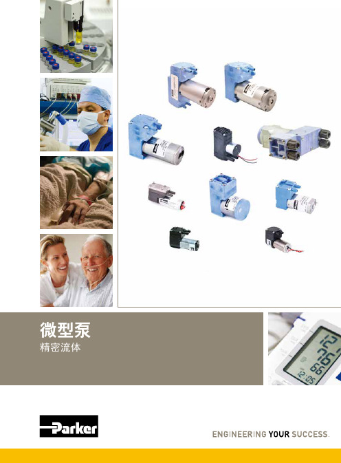
派克精密流体微型泵说明书
您与运动和控制技术领域的先行者合作,就是希望促进您的业务发展和全球的发展。
从微型电磁阀到高集成型自动化系统,我们的产品对于用于药物研发和病原体检测的救生医疗设备和科学仪器至关重要。
并且对于缩短上市时间和降低总体拥有成本也十分关键。
因此,请与派克合作,准备改变这一切吧!/precisionfluidics 1 603 595-1500目录页T2-05Helix124高效和紧凑型 13.5mm 宽泵 – 高达 800 mLPM高压泵 – 超过5.5 LPM 和高达100 PSI 的压力T2-0320高性能与尺寸比率泵 – 高达2.5 LPMLTC 系列76液体系列传送泵 – 高达 650 mLPMEZ 底座92振动隔离安装系统小型活塞泵(空气)微型泵(空气/气体)微型泵(液体)T2-0494超紧凑型、高效泵 – 高达 7.5LPMBTC-IIS 系列62应用广泛的多功能双头泵系列产品 – 高达 11 LPMBTC 系列52应用广泛的多功能泵系列产品 – 高达6 LPMLTC-IIS 系列84液体系列双头传送泵 – 高达1.5 LPMCTS 系列BTX-Connect 2836高性能紧凑型 20 mm 宽泵 – 高达 2.5 LPM多功能双头和单头泵系列,适合多种应用-高达10 LPMTTC 系列74紧凑、高效、低压泵 – 高达 6 LPMTTC-IIS 系列84紧凑、高效、低压双头泵 - 高达 11 LPM附件4Helix 微型高压泵高达100 PSI (6.9 bar)压力Parker Helix 是一款紧凑型高压泵,旨在实现小型即时临床护理仪器。
Helix 可在挑战性的高海拔环境和无法使用外部压缩空气的应用中实现高压操作。
Helix 泵可提供5.5 LPM 以上的流量和高达100 PSI (6.9 bar)的压力,为性能至关重要且空间有限的台式诊断设备提供了出色的解决方案。
• 集成了用于卸荷的X 阀,可实现高压重启• 内部飞轮可在高压下低速运行• 无油活塞• 简单的安装特性• 带有推入式接头的快速流体连接• 符合RoHS 指令和REACH 标准产品特性• 液上空气• 气动驱动•微流控芯片• 即时临床护理检验• 分子诊断• 核酸纯化•基因组学典型应用典型市场产品规格物理特性电子5微型隔Helix 微型高压泵典型流量曲线• 曲线展示了0.080"偏移泵的流量性能• 使用5.0 Vdc 控制输入时,泵将以大约4400 RPM 的转速和高达8.5 LPM的流量的状态运行,但不建议连续工作。
锂电池管理芯片LTC1960

1234SYMBOL PARAMETER CONDITIONS MIN TYP MAX UNITS t ONPI Gate B1I/B2I/DCI Turn-On Time V GS < –3V, C LOAD = 3nF (Note 5)300µs t OFFPI Gate B1I/B2I/DCI Turn-Off Time V GS > –1V, C LOAD = 3nF (Note 5)10µs V PONI Input Gate Clamp Voltage I LOAD = 1µAGB1I Highest (V BAT1 or V SCP) – V GB1I 4.75 6.77.5VGB2I Highest (V BAT2 or V SCP) – V GB2I 4.75 6.77.5VGDCI Highest (V DCIN or V SCP) – V GDCI 4.75 6.77.5V V POFFI Input Gate Off Voltage I LOAD = –25µAGB1I Highest (V BAT1 or V SCP) – V GB1I0.180.25VGB2I Highest (V BAT2 or V SCP) – V GB2I0.180.25VGDCI Highest (V DCIN or V SCP) – V GDCI0.180.25V Logic I/OI IH/I IL SSB/SCK/MOSI Input High/Low Current●–11µA V IL SSB/MOSI/SCK Input Low Voltage●0.8V V IH SSB/MOSI/SCK Input High Voltage●2V V OL MISO Output Low Voltage I OL = 1.3mA●0.4V I OFF MISO Output Off-State Leakage Current V MISO = 5V●2µA SPI Timing (See Timing Diagram)T WD Watch Dog Timer● 1.2 2.5 4.5sec t SSH SSB High Time680ns t CYC SCK Period C LOAD = 200pF R PULLUP = 4.7k on MISO●2µs t SH SCK High Time680ns t SL SCK Low Time680ns t LD Enable Lead Time200ns t LG Enable Lag Time200ns t su Input Data Set-Up Time●100ns t H Input Data Hold Time●100ns t A Access Time (From Hi-Z to Data Active on MISO)●125ns t dis Disable Time (Hold Time to Hi-Z State on MISO)●125ns t V Output Data Valid C L = 200pF, R PULLUP = 4.7k on MISO●580ns t HO Output Data Hold●0ns t Ir SCK/MOSI/SSB Rise Time0.8V to 2V250ns t If SCK/MOSI/SSB Fall Time2V to 0.8V250ns t Of MISO Fall Time2V to 0.4V, C L = 200 pF●400nsNote 1: Stresses beyond those listed under Absolute Maximum Ratings may cause permanent damage to the device. Exposure to any Absolute Maximum Rating condition for extended periods may affect device reliability and lifetime.Note 2. Battery voltage must be adequate to drive gates of PowerPath P-channel FET switches. This does not affect charging voltage of the battery, which can be zero volts.Note 3. See Test Circuit.Note 4. DCIN, BAT1, BAT2 are held at 12V and GDCI, GB1I, GB2I are forced to 10.5V. SCP is set at 12.0V to measure source current at GDCI,GB1I and GB2I. SCP is set at 11.9V to measure sink current at GDCI, GB1I and GB2I.Note 5. Extrapolated from testing with C L = 50pF.Note 6. VDAC offset is equal to the reference voltage, sinceV OUT = V REF(16mV • VDAC(VALUE)/2047 + 1).Note 7. The LTC1960C is guaranteed to meet specified performance from 0°C to 70°C and is designed, characterized and expected to meet specified performance at –40°C and 85°C, but is not tested at these extended temperature limits.ELECTRICAL CHARACTERISTICS The ●denotes specifications which apply over the full operating temperature range (Note 7), otherwise specifications are at T A = 25°C. V DCIN = 20V, V BAT1 = 12V, V BAT2 = 12V unless otherwise noted.51960fa6781960faInput Power RelatedSCN (Pin 4/Pin 30): PowerPath Current Sensing Negative Input. This pin should be connected directly to the “bot-tom” (output side) of the low valued resistor in series with the three PowerPath switch pairs, for detecting short-circuit current events. Also powers LTC1960 internal circuitry when all other sources are absent.SCP (Pin 5/Pin 31): PowerPath Current Sensing Positive Input. This pin should be connected directly to the “top”(switch side) of the low valued resistor in series with the three PowerPath switch pairs, for detecting short-circuit current events.GDCO (Pin 6/Pin 32): DCIN Output Switch Gate Drive.Together with GD CI, this pin drives the gate of the P-channel switch in series with the DCIN input switch.GDCI (Pin 7/Pin 33): D CIN Input Switch Gate D rive.Together with GDCO, this pin drives the gate of the P-channel switch connected to the DCIN input.GB1O (Pin 8/Pin 34): BAT1 Output Switch Gate Drive.Together with GB1I, this pin drives the gate of the P-channel switch in series with the BAT1 input switch.GB1I (Pin 9/Pin 35): BAT1 Input Switch Gate D rive.Together with GB1O, this pin drives the gate of the P-channel switch connected to the BAT1 input.GB2O (Pin 10/Pin 36): BAT2 Output Switch Gate Drive.Together with GB2I, this pin drives the gate of the P-channel switch in series with the BAT2 input switch.GB2I (Pin 11/Pin 37): BAT2 Input Switch Gate D rive.Together with GB2O, this pin drives the gate of the P-channel switch connected to the BAT2 input.CLP (Pin 24/Pin 13): This is the Positive Input to the Supply Current Limiting Amplifier CL1. The threshold is set at 100mV above the voltage at the DCIN pin. When used to limit supply current, a filter is needed to filter out the switching noise.Battery Charging RelatedV SET (Pin 13/Pin 1): The Tap Point of a Programmable Resistor Divider which Provides Battery Voltage Feedback to the Charger. A capacitor from CSN to V SET and one from V SET to GND provide necessary compensation and filter-ing for the voltage loop.I TH (Pin 14/Pin 2): This is the Control Signal of the Inner Loop of the Current Mode PWM. Higher I TH corresponds to higher charging current in normal operation. A capaci-tor of at least 0.1µF to GND filters out PWM ripple. Typical full-scale output current is 30µA. Nominal voltage range for this pin is 0V to 2.4V.I SET (Pin 15/Pin 3): A Capacitor from I SET to Ground is Required to Filter Higher Frequency Components from the Delta-Sigma IDAC.CSN (Pin 22/Pin 11): Current Amplifier CA1 Input. Con-nect this to the common output of the charger MUX switches.CSP (Pin 23/Pin 12): Current Amplifier CA1 Input. This pin and the CSN pin measure the voltage across the sense resistor, RSNS, to provide the instantaneous current signals required for both peak and average current mode operation.COMP1 (Pin 25/Pin 14): This is the Compensation Node for the Amplifier CL1. A capacitor is required from this pin to GND if input current amplifier CL1 is used. At input adapter current limit, this node rises to 1V. By forcing COMP1 low, amplifier CL1 will be defeated (no adapter current limit). COMP1 can source 10µA.BGATE (Pin 27/Pin 16): D rives the Bottom External MOSFET of the Battery Charger Buck Converter.SW (Pin 30/Pin 19): Connected to Source of Top External MOSFET Switch. Used as reference for top gate driver.BOOST (Pin 31/Pin 20): Supply to Topside Floating Driver.The bootstrap capacitor is returned to this pin. Voltage swing at this pin is from a diode drop below V CC to (DCIN + V CC ).PI FU CTIO SU U U(G/UHF)91960faTGATE (Pin 32/Pin 21): Drives the Top External MOSFET of the Battery Charger Buck Converter.SCH1 (Pin 33/Pin 22), SCH2 (Pin 36/Pin 25): Charger MUX Switch Source Returns. These two pins are con-nected to the sources of Q3/Q4 and Q9/Q10 (see Typical Application on back page of data sheet), respectively. A small pull-down current source returns these nodes to 0V when the switches are turned off.GCH1 (Pin 34/Pin 23), GCH2 (Pin 35/Pin 24): Charger MUX Switch Gate Drives. These two pins drive the gates of the back-to-back N-channel switch pairs, Q3/Q4 and Q9/Q10, between the charger output and the two batteries.External Power Supply PinsV PLUS (Pin 1/Pin 27): Supply. The V PLUS pin is connected via four internal diodes to the DCIN, SCN, BAT1, and BAT2 pins. Bypass this pin with a 1µF to 2µF capacitor.BAT1 (Pin 3/Pin 29), BAT2 (Pin 2/Pin 28): These two pins are the inputs from the two batteries for power to the LTC1960 and to provide voltage feedback to the battery charger.LOPWR (Pin 12/Pin 38): LOPWR Comparator Input from External Resistor Divider Connected from SCN to GND. If the voltage at LOPWR is lower than the LOPWR com-parator threshold, then system power has failed and power is autonomously switched to a higher voltage source, if available. See PowerPath section of LTC1960operation.DCDIV (Pin 17/Pin 5): DCDIV Comparator Input from External Resistor D ivider Connected from D CIN to GND . If the voltage at D CD IV is above the D CD IV comparator threshold, then the D C bit is set and the wall adapter power is considered to be adequate to charge the batteries. If DCDIV is taken more than 1.8Vabove V CC , then all of the power path switches are latched off until all power is removed.DCIN (Pin 29/Pin 18): Supply. External DC power source.A 1µF bypass capacitor should be connected to this pin as close as possible. No series resistance is allowed,since the adapter current limit comparator input is also this pin.Internal Power Supply PinsGND (Pin 16/Pin 4, Pin 10, Pin 26, Pin 39): Ground for Low Power Circuitry.PGND (Pin 26/Pin 15): High Current Ground Return for BGATE Driver.V CC (Pin 28/Pin 17): Internal Regulator Output. Bypass this output with at least a 2µF to 4.7µF capacitor. Do not use this regulator output to supply more than 1mA to external circuitry.Digital Interface PinsSSB (Pin 18/Pin 6): SPI Slave Select Input. Active low.TTL levels. This signal is low when clocking data to/from the LTC1960.SCK (Pin 19/Pin 7): Serial SPI Clock. TTL levels.MISO (Pin 20/Pin 8): SPI Master-In-Slave-Out Output,Open Drain. Serial data is transmitted from the LTC1960,when SSB is low, on the falling edge of SCK. TTL levels.A 4.7k pullup resistor is recommended.MOSI (Pin 21/Pin 9): SPI Master-Out-Slave-In Input.Serial data is transmitted to the LTC1960, when SSB is low, on the rising edge of SCK. TTL levels.Exposed Pad (Pin 39, UHF Package Only): Ground.Must be soldered to the PCB ground for rated thermal performance.PI FU CTIO SU U U(G/UHF)10OVERVIEWThe LTC1960 is composed of a battery charger controller, charge MUX controller, PowerPath controller, SPI inter-face, a 10-bit current DAC (IDAC) and 11-bit voltage DAC (VDAC). When coupled with a low cost microprocessor, it forms a complete battery charger/selector system for two batteries. The battery charger is programmed for voltage and current, and the charging battery is selected via the SPI interface. Charging can be accomplished only if the voltage at DCDIV indicates that sufficient voltage is avail-able from the input power source, usually an AC adapter. The charge MUX, which selects the battery to be charged, is capable of charging both batteries simultaneously by selecting both batteries for charging. The charge MUX switch drivers are configured to allow charger current to share between the two batteries and to prevent current from flowing in a reverse direction in the switch. The amount of current that each battery receives will depend upon the relative capacity of each battery and the battery voltage. This can result in significantly shorter charging times (up to 50% for Li-Ion batteries) than sequential charging of each battery. In order to continue charging, the CHARGE_BAT information must be updated more frequently than the internal watchdog timer.The PowerPath controller selects which of the pairs of PFET switches, input and output, will provide power to the system load. The selection is accomplished over the SPI interface. If the system voltage drops below the threshold set by the LOPWR resistor divider, then all of the output side PFETs are turned on quickly and power is taken from the highest voltage source available at the DCIN, BAT1 or BAT2 inputs. The input side PFETs act as diodes in this mode and power is taken from the source with the highest voltage. The input side PowerPath switch driver that is delivering power then closes its input switch to reduce the power dissipation in the PFET bulk diode. In effect, this system provides diode -like behavior from the FET switches, without the attendant high power dissipation from diodes. The microprocessor is informed of this 3-diode mode status when it polls the PowerPath status register via the SPI interface. The microprocessor can then assess which power source is capable of providing power, and program the PowerPath switches accordingly. Since high speed PowerPath switching at LOPWR trip points is handled autonomously, there is no need for real-time microproces-sor resources to accomplish this task. Simultaneous discharge of both batteries is accomplished by simply programming both batteries for discharge into the system load. The switch drivers prevent reverse cur-rent flow in the switches and automatically discharge both batteries into the load, sharing current according to the relative capacity of the batteries. Simultaneous dual dis-charge can increase battery operating time by approxi-mately 10% by reducing losses in the switches and reducing internal losses associated with high discharge rates. SPI InterfaceThe SPI interface is used to write to the internal PowerPath registers, the charger control registers, the current DAC, and the voltage DAC. The SPI is also able to read internal status registers. There are two types of SPI write com-mands. The first write command is a 1-byte command used to load PowerPath and charger control bits. The second write command is a 2-byte command used to load the DACs. The SPI read command is a 2-byte command. In order to ensure the integrity of the SPI communication, the last bit received by the SPI is echoed back over the MISO output after the next falling SCK. The data format is set up so that the master has the option of aborting a write if the returned MISO bit is not as expected.1-Byte SPI Write Format:bit 7........byte 1..........bit 0 MOSI D0 D1 D2 X A0 A1 A2 0 MISO X D0 D1 D2 X A0 A1 A2 Charger Write Address:A[2:0] = b111Charger Write Data:D2 = XD1 = CHARGE_BAT2D0 = CHARGE_BAT1PowerPath Write Address:A[2:0] = b110PowerPath Write Data:D2 = POWER_BY_DCD1 = POWER_BY_BAT2D0 = POWER_BY_BAT1OPERATIO(Refer to Block Diagram and Typical Application)111960fa121960fa2-Byte SPI Write Format:bit 7........byte 1..........bit 0 bit 7..........byte 2............bit 0MOSI D0 D1 D2 D3 D4 D5 D6 1 D7 D8 D9 D10 A0 A1 A2 0MISOX D0 D1 D2 D3 D4 D5 D6 1 D7 D8 D9 D10 A0 A1 A2IDAC Write Address:A[2:0] = b000IDAC Data Bits D9-D0:IDAC value data (MSB-LSB)IDAC Data Bit D10 :Normal mode = 0, low current mode = 1 (Dual battery charging is disabled)VDAC Write Address:A[2:0] = b001VDAC Data Bits D10-D0:VDAC value (MSB-LSB)Subsequent SPI communication is inhibited until after the addressed DAC is finished loading. It is recommended that the master transmit all zeros until MISO goes low. This handshaking procedure is illustrated in Figure 1.2-Byte SPI Read Format:bit 7........byte 1.......bit 0bit 7........byte 2............bit 0MOSI 0 0 0 0 A0 A1 A2 0 0 0 0 0 A0 A1 A2 1MISO X 0 0 0 0 A0 A1 A2 X FA LP DC PF CH X XStatus Address:A[2:0] = b010Status Read Data:LP = LOW_POWER (Low power comparator output)DC = DCDIV (DCDIV comparator output)PF = POWER_FAIL (Set if selected power supply failed to hold up system power after three tries)CH = CHARGING (One or more batteries are being charged)FA = FAULT. This bit is set for any of the following conditions:1) The LTC1960 is still in power on reset.2) The LTC1960 has detected a short circuit and has shut down power and charging.3) The system has asserted a fast off using DCDIV.Figure 1. SPI Write to VDAC of Data = b101_0101_0101Note: All other values of A[2:0] are reserved and must not be used.OPERATIOSSBSCKMOSIMISO1960 F01BYTE 1BYTE 2Figure 2. SPI Read of FA = 0, LP = 0, DC = 1, PF = 0, and CH = 1Battery Charger ControllerThe LTC1960 charger controller uses a constant off-time, current mode step-down architecture. During normal op-eration, the top MOSFET is turned on each cycle when the oscillator sets the SR latch and turned off when the main current comparator I CMP resets the SR latch. While the top MOSFET is off, the bottom MOSFET is turned on until either the inductor current reverses, as indicated by cur-rent comparator IREV, or the beginning of the next cycle. The oscillator uses the equation:t OFF = 1/f OSC • (V DCIN – V CSN)/V DCINto set the bottom MOSFET on time. The peak inductor current at which ICMP resets the SR latch is controlled by the voltage on I TH. I TH is in turn controlled by several loops, depending upon the situation at hand. The average current control loop converts the voltage between CSP and CSN to a representative current. Error amp CA2 compares this current against the desired current requested by the IDAC at the I SET pin and adjusts I TH until the ID AC value is satisfied. The BAT1/BAT2 MUX provides the selected battery voltage at CHGMON, which is divided down to the V SET pin by the VDAC resistor divider and is used by error amp EA to decrease I TH if the V SET voltage is above the 0.8V reference. The amplifier CL1 monitors and limits the input current, normally from the AC adapter, to a preset level (100mV/R CL). At input current limit, CL1 will decrease the I TH voltage and thus reduce battery charging current. An overvoltage comparator, 0V, guards against transient overshoots (>7%). In this case, the top MOSFET is turned off until the overvoltage condition is cleared. This feature is useful for batteries which “load dump”themselves by opening their protection switch to perform functions such as calibration or pulse mode charging.Charging is inhibited for battery voltages below the mini-mum charging threshold, V CHMIN. Charging is not inhib-ited when the low current mode of the IDAC is selected. The top MOSFET driver is powered from a floating boot-strap capacitor C B. This capacitor is normally recharged from V CC through an external diode when the top MOSFET is turned off. A 2µF to 4.7µF capacitor across V CC to GND is required to provide a low dynamic impedance to charge the boost capacitor. It is also required for stability and power-on-reset purposes.As V IN decreases towards the selected battery voltage, the converter will attempt to turn on the top MOSFET continu-ously (“dropout’’). A dropout timer detects this condition and forces the top MOSFET to turn off, and the bottom MOSFET on, for about 200ns at 40µs intervals to recharge the bootstrap capacitor.Charge MUX SwitchesThe equivalent circuit of a charge MUX switch driver is shown in Figure 3. If the charger controller is not enabled, the charge MUX drivers will drive the gate and source of the series connected MOSFETs to a low voltage and the switch is off. When the charger controller is on, the charge MUX driver will keep the MOSFETs off until the voltage at CSN rises at least 35mV above the battery voltage. GCH1 is then driven with an error amplifier EAC until the voltage between BAT1 and CSN satisfies the error amplifier or until GCH1 is clamped by the internal Zener diode. The time required to close the switch could be quite long (many ms) due to the small currents output by the error amp and depending upon the size of the MOSFET switch.If the voltage at CSN decreases below V BAT1 – 20mV a comparator CC quickly turns off the MOSFETs to preventOPERATIOA status read is illustrated in Figure 2.SSBSCKMOSIMISOBYTE 1BYTE 2131960fa14151617181960faWatchdog TimerCharging will begin when either CHARGE_BAT1 or CHARGE_BAT2 bits are set in the charger register (address: 111). Charging will stop if the charger register is not updated prior to the expiration of the watchdog timer.Simply repeating the same data transmission to the charger register at a rate higher than once per second will ensure that charging will continue uninterrupted.Extending System to More than 2 BatteriesThe LTC1960 can be extended to manage systems with more than 3 sources of power. Contact Linear Technology Applications Engineering for more information.Charging Depleted BatteriesSome batteries contain internal protection switches that disconnect a load if the battery voltage falls below what is considered a reasonable minimum. In this case, the charger may not start because the voltage at the battery terminal is less than 5V. The low current mode of the IDAC must be used in this case to condition the battery. In low current mode, there is no minimum voltage requirement (but dual charging is not allowed). Usually, the battery will detect that it is being charged and then close its protection switch, which will allow the ID AC to switch to normal mode. Smart batteries require that charging current not exceed 100mA until valid charging voltage and charging current parameters are transmitted via the SMBus. The low current IDAC mode is ideal for this purpose.Starting Charge with Dissimilar Batteries in Dual Charge ModeWhen charging batteries of different charger termination voltages, the charger should be started using the following procedure:Step 1. Select only the lowest termination voltage battery for charging, and set the charger to its charging param-eters.Step 2. When the battery current is flowing into that battery, change to dual charging mode (without stopping the charger) and set the appropriate charging parameters for this dual charger condition.APPLICATIO S I FOR ATIO W UU U If this procedure is not followed, and BAT2 is significantly higher voltage than BAT1, the charger could refuse to charge either battery.Charge Termination IssuesBatteries with constant-current charging and voltage-based charger termination might experience problems with reductions of charger current caused by adapter limiting. It is recommended that input limiting feature be defeated in such cases. Consult the battery manufacturer for information on how your battery terminates charging.Setting Output Current LimitThe full scale output current setting of the ID AC will produce V MAX = 102.3mV between CSP and CSN. To set the full scale current of the DAC simply divide V MAX by R SNS .This is expressed by the following equation:R SNS = 0.1023/I MAXTable 1. Recommended R SNS Resistor ValuesI MAX (A)R SNS (Ω) 1%R SNS (W)1.0230.1000.252.0460.0500.254.0920.0250.58.1840.0121Use resistors with low ESL.Inductor SelectionHigher operating frequencies allow the use of smaller inductor and capacitor values. A higher frequency gener-ally results in lower efficiency because of MOSFET gate charge losses. In addition, the effect of inductor value on ripple current and low current operation must also be considered. The inductor ripple current ∆I L decreases with higher frequency and increases with higher V IN .∆I f L V V V L OUT OUT IN =()()−⎛⎝⎜⎞⎠⎟11Accepting larger values of ∆I L allows the use of low inductances, but results in higher output voltage ripple191960faand greater core losses. A reasonable starting point for setting ripple current is ∆I L = 0.4(I MAX ). In no case should ∆I L exceed 0.6(I MAX ) due to limits imposed by IREV and CA1. Remember the maximum ∆I L occurs at the maxi-mum input voltage. In practice 10µH is the lowest value recommended for use.Charger Switching Power MOSFET and Diode SelectionTwo external power MOSFETs must be selected for use with the LTC1960 charger: An N-channel MOSFET for the top (main) switch and an N-channel MOSFET for the bottom (synchronous) switch.The peak-to-peak gate drive levels are set by the V CC voltage. This voltage is typically 5.2V. Consequently, logic-level threshold MOSFETs must be used. Pay close atten-tion to the B VDSS specification for the MOSFETs as well;many of the logic level MOSFETs are limited to 30V or less.Selection criteria for the power MOSFETs include the “ON”resistance R DS(ON), reverse transfer capacitance C RSS ,input voltage and maximum output current. The LTC1960charger is always operating in continuous mode so the duty cycles for the top and bottom MOSFETs are given by:Main Switch Duty Cycle = V OUT /V INSynchronous Switch Duty Cycle = (V IN – V OUT )/V IN The MOSFET power dissipations at maximum output current are given by:P MAIN = V OUT /V IN (I MAX )2(1 + δ∆Τ)R DS(ON) + k(V IN )2(I MAX )(C RSS )(f)P SYNC = (V IN – V OUT )/V IN (I MAX )2(1 + δ∆Τ) R DS(ON)Where δ∆Τ is the temperature dependency of R DS(ON) and k is a constant inversely related to the gate drive current.Both MOSFETs have I 2R losses while the topside N-channel equation includes an additional term for transi-tion losses, which are highest at high input voltages. For V IN < 20V the high current efficiency generally improves with larger MOSFETs, while for V IN > 20V the transition losses rapidly increase to the point that the use of a higher R DS(ON) device with lower C RSS actually provides higher efficiency. The synchronous MOSFET losses are greatest at high input voltage or during a short-circuit whenAPPLICATIO S I FOR ATIO W UU U the duty cycle in this switch is nearly 100%. The term (1 + δ∆Τ) is generally given for a MOSFET in the form of a normalized R DS(ON) vs Temperature curve, but δ = 0.005/°C can be used as an approximation for low voltage MOSFETs.C RSS is usually specified in the MOSFET characteristics.The constant k = 1.7 can be used to estimate the contribu-tions of the two terms in the main switch dissipation equation.If the LTC1960 charger is to operate in low dropout mode or with a high duty cycle greater than 85%, then the topside N-channel efficiency generally improves with a larger MOSFET. Using asymmetrical MOSFETs may achieve cost savings or efficiency gains.The Schottky diode D1, shown in the Typical Application on the back page, conducts during the dead-time between the conduction of the two power MOSFETs. This prevents the body diode of the bottom MOSFET from turning on and storing charge during the dead-time, which could cost as much as 1% in efficiency. A 1A Schottky is generally a good size for 4A regulators due to the relatively small average current. Larger diodes can result in additional transition losses due to their larger junction capacitance.The diode may be omitted if the efficiency loss can be tolerated.Calculating I C Power DissipationThe power dissipation of the LTC1960 is dependent upon the gate charge of Q TG and Q BG .(Refer to Typical Application). The gate charge is determined from the manufacturer’s data sheet and is dependent upon both the gate voltage swing and the drain voltage swing of the FET.P D = (V DCIN – V VCC )([f OSC (Q TG + Q BG ) + I VCC ]+ V DCIN • I DCIN )Example: V VCC = 5.2V, V DCIN = 19V, f OSC = 345kHz,Q G2 = Q G3 = 15nC, I VCC = 0mA.P D = 165mW V SET /I SET CapacitorsCapacitor C7 is used to filter the delta-sigma modulation frequency components to a level which is essentially DC.Acceptable voltage ripple at ISET is about 10mV P-P . Since the period of the delta-sigma switch closure, T ∆Σ, is about201960fa10µs and the internal IDAC resistor, R SET , is 18.77k, the ripple voltage can be approximated by:∆∆V V T R C ISET REF SET =∑••7Then the equation to extract C7 is: C V T V R REF ISET SET7=∑••∆∆= 0.8/0.01/18.77k(10µs) ≅ 0.043µFIn order to prevent overshoot during start-up transients the time constant associated with C7 must be shorter than the time constant of C5 at the I TH pin. If C7 is increased to improve ripple rejection, then C5 should be increased proportionally and charger response time to average cur-rent variation will degrade.Capacitor C B1 and C B2 are used to filter the VDAC delta-sigma modulation frequency components to a level which is essentially DC. C B2 is the primary filter capacitor and CB1 is used to provide a zero in the response to cancel the pole associated with C B2. Acceptable voltage ripple at V SET is about 10mV P-P . Since the period of the delta-sigma switch closure, T ∆Σ, is about 11µs and the internal VDAC resistor, R VSET , is 7.2k Ω, the ripple voltage can be ap-proximated by:∆∆V V T R C C VSET REF VSET B B =()∑•||12Then the equation to extract C B1 || C B2 is:C C V T R V B B REF VSET VSET12||•=∑∆∆C B2 should be 10× to 20× C B1 to divide the ripple voltage present at the charger output. Therefore C B1 = 0.01µF and C B2 = 0.1µF are good starting values. In order to prevent overshoot during start-up transients the time constant associated with C B2 must be shorter than the time constant of C5 at the I TH pin. If C B2 is increased to improve ripple rejection, then C5 should be increased proportionally and charger response time to voltage variation will degrade.Input and Output CapacitorsIn the 4A Lithium Battery Charger (Typical Application section), the input capacitor (C IN ) is assumed to absorb all input switching ripple current in the converter, so it must have adequate ripple current rating. Worst-case RMS ripple current will be equal to one half of output charging current. Actual capacitance value is not critical. Solid tantalum low ESR capacitors have high ripple current rating in a relatively small surface mount package, but caution must be used when tantalum capacitors are used for input or output bypass . High input surge currents can be created when the adapter is hot-plugged to the charger or when a battery is connected to the charger. Solid tantalum capacitors have a known failure mechanism when subjected to very high turn-on surge currents. Only Kemet T495 series of “Surge Robust” low ESR tantalums are rated for high surge conditions such as battery to ground.The relatively high ESR of an aluminum electrolytic for C15, located at the AC adapter input terminal, is helpful in reducing ringing during the hot-plug event.Highest possible voltage rating on the capacitor will mini-mize problems. Consult with the manufacturer before use.Alternatives include new high capacity ceramic (at least 20µF) from Tokin, United Chemi-Con/Marcon, et al. Other alternative capacitors include OSCON capacitors from Sanyo.The output capacitor (C OUT ) is also assumed to absorb output switching current ripple. The general formula for capacitor current is:I RMS = (L1)(f)V BATV DCIN()0.29 (V BAT ) 1 –For example:V DCIN = 19V, V BAT = 12.6V, L1 = 10µH, and f = 300kHz, I RMS = 0.41A.EMI considerations usually make it desirable to minimize ripple current in the battery leads, and beads or inductors may be added to increase battery impedance at the 300kHzAPPLICATIO S I FOR ATIO W UU U。
CSI Solar HiKu高功率单晶微晶模块说明书

CS3W-445|450|455|460|465|470MSMORE POWER445 W ~ 470 W* For detailed information, please refer to Installation Manual.CSI Solar Co., Ltd. is committed to providing high quality solar photovoltaic modules, solar energy and battery storage solutions to customers. The company was recognized as the No. 1 module supplier for quality and performance/price ratio in the IHS Module Customer Insight Survey. Over the past 20 years, it has successfully delivered over 70 GW of premium-quality solar modules across the world.HiKuHIGH POWER MONO PERC MODULE26 % more power than conventional modules Low NMOT: 41 ± 3 °CLow temperature coefficient (Pmax): -0.34 % / °CMORE RELIABLEUp to 4.5 % lower LCOEUp to 2.7 % lower system cost Heavy snow load up to 5400 Pa, wind load up to 3600 Pa*41°CBetter shading toleranceLower internal current, lower hot spot temperatureMinimizes micro-crack impactsIEC 61215 / IEC 61730 / CE / MCS / INMETRO / UKCA FSEC (US Florida) / UL 61730 / IEC 61701 / IEC 62716 UNI 9177 Reaction to Fire: Class 1 / Take-e-wayPRODUCT CERTIFICATES*ISO 9001:2015 / Quality management systemISO 14001:2015 / Standards for environmental management systemISO 45001: 2018 / International standards for occupational health & safetyMANAGEMENT SYSTEM CERTIFICATES**According to the applicable Canadian Solar Limited Warranty Statement.12YearsYears1st year power degradation no more than 2%Subsequent years: annual power degradation no more than 0.55%Enhanced Product Warranty on Materialsand Workmanship*Linear Power Performance Warranty*CSI Solar Co., Ltd.199LushanRoad,SND,Suzhou,Jiangsu,China,215129,,********************* The specific certificates applicable to different module types and markets will vary, and therefore not all of the certifications listed herein will simultaneously apply to the products you order or use. Please contact your local Canadian Solar sales repre -sentative to confirm the specific certificates available for your product and applicable in the regions in which the products will be used.PARTNER SECTIONELECTRICAL DATA | STC*CS3W445MS 450MS 455MS 460MS 465MS 470MS Nominal Max. Power (Pmax)445 W450 W 455 W 460 W 465 W 470 W Opt. Operating Voltage (Vmp)40.9 V41.1 V 41.3 V 41.5 V 41.7 V 41.9 V Opt. Operating Current (Imp)10.89 A 10.96 A 11.02 A 11.09 A 11.16 A 11.22 A Open Circuit Voltage (Voc)48.9 V 49.1 V 49.3 V 49.5 V 49.7 V 49.9 V Short Circuit Current (Isc)11.54 A 11.60 A 11.66 A 11.72 A 11.78 A 11.84 AModule Efficiency 20.1%20.4%20.6%20.8%21.0%21.3%Operating Temperature -40°C ~ +85°CMax. System Voltage 1500V (IEC/UL) or 1000V (IEC/UL)Module Fire Performance TYPE 1 (UL 61730 1500V) or TYPE 2 (UL 61730 1000V) or CLASS C (IEC 61730)Max. Series Fuse Rating 20 A Application Classification Class A Power Tolerance* Under Standard Test Conditions (STC) of irradiance of 1000 W/m 2, spectrum AM 1.5 and cell temperature of 25°C.ELECTRICAL DATA | NMOT*CS3W445MS 450MS 455MS 460MS 465MS 470MS Nominal Max. Power (Pmax)334 W 338 W341 W 345 W 349 W 353 W Opt. Operating Voltage (Vmp)38.3 V38.5 V 38.7 V 38.9 V 39.1 V 39.3 V Opt. Operating Current (Imp)8.71 A 8.76 A 8.82 A 8.87 A 8.92 A 8.98 A Open Circuit Voltage (Voc)46.2 V 46.4 V 46.6 V 46.8 V 47.0 V 47.2 V Short Circuit Current (Isc)9.31 A9.35 A9.40 A9.45 A9.50 A9.55 A* Under Nominal Module Operating Temperature (NMOT), irradiance of 800 W/m 2, spectrum AM 1.5, ambient temperature 20°C, wind speed 1 m/s.CS3W-445MS / I-V CURVESMECHANICAL DATA Specification DataCell TypeMono-crystalline Cell Arrangement 144 [2 X (12 X 6) ]Dimensions 2108 X 1048 X 35 mm (83.0 X 41.3 X 1.38 in)Weight 24.3 kg (53.6 lbs)Front Cover 3.2 mm tempered glass with anti-ref-lective coatingFrame Anodized aluminium alloy J-BoxIP68, 3 bypass diodesCable 4 mm 2 (IEC), 12 AWG (UL)Cable Length (Including Connector)500 mm (19.7 in) (+) / 350 mm (13.8 in) (-) or customized length*ConnectorT6 or T4 series or MC4-EVO2 or MC4-EVO2APer Pallet 30 pieces Per Container (40' HQ)660 pieces* For detailed information, please contact your local Canadian Solar sales and technical representatives.TEMPERATURE CHARACTERISTICS SpecificationData Temperature Coefficient (Pmax)-0.34 % / °C Temperature Coefficient (Voc)-0.26 % / °C Temperature Coefficient (Isc)0.05 % / °CNominal Module Operating Temperature 41 ± 3°CVA1211109876543210 5 10 15 20 25 30 35 40 45 50 V A5 10 15 20 25 30 35 40 45 501000 W/m 800 W/m600 W/m 400 W/m200 W/m5°C 25°C 45°C 65°C1211109876543210 ~ + 10 WSept. 2022. All rights reserved, PV Module Product Datasheet V6.0_ENCSI Solar Co., Ltd.199LushanRoad,SND,Suzhou,Jiangsu,China,215129,,********************* The specifications and key features contained in this datasheet may deviate slightly from our actual products due to the on-going innovation and product enhancement .CSI Solar Co., Ltd. reserves the right to make neces-sary adjustment to the information described herein at any time without further notice.Please be kindly advised that PV modules should be handled and installed by qualified people who have profes -sional skills and please carefully read the safety and installation instructions before using our PV modules.ENGINEERING DRAWING (mm)Rear ViewMounting HoleA-AB-BFrame Cross SectionLength: ±2mm Width: ±2mmHeight: ±1mm。
LTC1664_1资料

W
1
元器件交易网
LTC1664 ABSOLUTE
(Note 1)
AXI U
RATI GS
PACKAGE/ORDER I FOR ATIO
TOP VIEW GND VOUT A VOUT B VOUT C VOUT D REF CS/LD SCK 1 2 3 4 5 6 7 8 16 VCC 15 NC 14 NC 13 NC 12 NC 11 CLR 10 DOUT 9 DIN
CONTROL LOGIC REF CS/LD SCK 6 7 8
ADDRESS DECODER 11 10 9 CLR DOUT DIN
1664 BD
–0.4 –0.6 –0.8
SHIFT REGISTER
–1.0 0 256 512 CODE 768 1023
1664 G08
U
Differential Nonlinearity (DNL)
BLOCK DIAGRA
GND 1 10-BIT DAC A
16 VCC 10-BIT DAC D 5 VOUT D
1.0 0.8 0.6 VCC = 5V VREF = 4.096V
VOUT A
2
VOUT B
3
10-BIT DAC B
10-BIT DAC C
4
VOUT C
LSB
0.4 0.2 0 –0.2
, LTC and LT are registered trademarks of Linear Technology Corporation.
U APPLICATIO S
s s s s s
Mobile Communications Remote Industrial Devices Automatic Calibration for Manufacturing Portable Battery-Powered Instruments Trim/Adjust Applications
Lincoln Power TIG 275 焊接机说明书

ProcessesStick, TIGProduct NumberK2619-1K2619-2K2620-1K2618-1 Ready-Pak®Package See back for complete specs© Lincoln Global, Inc. All Rights Reserved.275TIG WELDERSInput Power (Voltage/Phase/Hertz)K2619-1/K2618-1:208/230/460/1/60K2619-2:460/575/1/60K2620-1:220-230/380-400/415/1/50/60Input Current at Rated Output208V:104460V:47220-230V:95575V:38230V:94380-400V:55415V:50Rated Output: Current/Voltage/Duty Cycle275A/31V/40%Weight/Dimensions (H x W x D)397 lbs. (180 kg)31 x 22 x 26 in.(787 x 559 x 660 mm)INPUT OUTPUTK2618-1 Includes:K2619-1Under-Cooler Cart Water Cooler –PH: +1.216-481-8100 • LI NC OL N E L E C TR ICShown K2619-1[ 2]|Precision TIG ®275What Is It?Pulse welding systems vary weld current between peak (high heat) and background current (low heat) levels. Adjusting the pulse frequency controls the level of heat input applied to the weld relative to the weld travel speed.ResultsBetter control of heat input in the weld, resulting in:•Reduced warping and burnthrough on thin materials. •Smaller heat-affected zone – good for thin material.•Smaller bead profile without compromising proper penetration.Easy “Set It/See It” Operation:•Flashing indicator light lets you see the pulse rate before you strike an arc.W e l d i n g C u r r e ntTimePulsed TIG Weld (at 60 amps)Standard TIG Weld (at 60 amps) Smaller HeatAffected ZoneSmaller Bead ProfileMicro-Start ™II Technology aids arc stabilityTHROUGHOUT THE WELD CYCLE – even at the lowest amperage! Micro-Start ™II Technologycontrolled ramp down helps precisely fill the weld crater for quality results.Micro-Start ™II Technology minimizes high frequency and ‘hot starts’ to deliver soft arc starts without arc wandering for AC and DC welding. Arc PerformanceMicro-Start ™Stable, Focused Arc Precise Crater Fill“Set It/See It” Pulse Control — Make attractive and consistent welds!N O WIN C L U D ESf o r A L UM IN U MW E L D INGA CPrecision TIG ®275| [ 3]AC Auto Balance ®Controls —Automatically sets the optimal cleaning vs. penetration level for aluminum welding!What Is It?When aluminum welding, the positive (+) portion of the AC weldingamperage cleans the oxides from the aluminum surface. The negative (-)portion delivers more heat input, increasing penetration level.Patented AC Auto Balance ®automatically sets the ratio of cleaning action (+) versus penetration (-) based on amperage.Manual balance control provides the flexibility to customize the arc to your preference.Easy Operation:•Set it and forget it or override when you choose to customize the settings.More Cleaning (+)Less Cleaning (+)Less Penetration(-)More Penetration (-)W E L D I N G W E L D I N G TIMETIMEMaximum Cleaning SettingMaximum Penetration SettingAuto Balance Setting•Fan-As-Needed (F.A.N.)™minimizes repeated heating and cooling of internal components, keeps dust and dirt build-up to a minimum and saves on electricity costs. •Engineered cooling air routing brings clean air in from the top and exhausts at the bottom to draw and collect less dirt in the machine. •Compare these reliability enhancing design features: — Crimped and soldered power connections.— Wound and varnished electrical coils do not require coil spacers used on competitive models. — Locking tabs on PC board connectors eliminates loose connections.•Tough testing cycles ensure long service — dropping, jerking,rolling, shipping, vibration, resistance to real world extreme conditions, and extended in-service life testing. •CSA C/US certified.•Lincoln three-year warranty on parts and labor.Clean, cool air route shown.Snap-action durable switches make positive mechanical contact to reduce chances ofintermittent contact failure.[ 4]| Precision TIG ®275Shown: K2618-1Water-Cooled Ready-Pak ®PackageTorch Parts Storage Compartment.Optional TIG pulsing helps you make great welds.Water-cooled torch connections with no adapters — side mounted to keep out of the way and protected.Neat/organized cable management with integratedtorch holster.Separate output studs for stick and TIG keep both stick electrode holder and TIG torch connected at the same time — eliminates set-up changeover when switching processes.Easily accessible input voltagereconnect panel.Low-Lift ™ Shielding Gas Bottle Platform.Lockable Undercarriage Storage and Water Cooler Drawers.Reliable Pro-Con Pump.Optional Features:(standard with K2618-1 Water-Cooled Ready-Pak ®Package)Precision TIG ®275| [ 5]Large, well-spaced controls make it easy to view and set upwith gloved hands.SET-UP MENUPress and hold the menu button to display up to seven programmable parameters. The setting of the desired level is displayed, and increasing or decreasing the level setting is easy.The Set-Up Menu includes:Standard•DC TIG Start Modes: High Frequency, Scratch Start, and Touch Start TIG ®.•Adjustable Preflow Time.•Adjustable Start Pulse for Soft or Forceful Starts.With Optional Advanced Control Panel •Adjustable TIG Hot Start.•Adjustable Upslope Time.•Adjustable Stick Hot Start.•Adjustable Stick Arc Force.A)Minimum Output Control & Display Switch (Also displays output voltage)B)Set-Up Menu (see below)C)Digital MeterD)Local/Remote Current Control Switch E)Maximum Output Control F)Post Flow Time G)Thermal Shutdown Light H)Optional Advanced Control Panel 1)Trigger Switch (2-step/4-step)2)Pulse/Spot Time Mode Switch 3)Pulse Frequency Control 4)Pulse % On Time Control 5)Pulse Background Current Control 6)Downslope Time, In Seconds 7)Spot Time I)Polarity Switch J)Power Switch K)AC Balance Control L)Mode SwitchH123 4 & 756BCDEAF G HI J KLC U S T O M E R A S S I S T A N C E P O L I C YThe business of The Lincoln Electric Company ®is manufacturing and selling high quality welding equipment, consumables, and cutting equipment. Our challenge is to meet the needs of our customers and to exceed their expectations. On occasion, purchasers may ask Lincoln Electric for information or advice about their use of our products. Our employees respond to inquiries to the best of their ability based on information provided to them by the customers and the knowledge they may have concerning the application. Our employees, however, are not in a position to verify the information provided or to evaluate the engineering requirements for the particular weldment. Accordingly, Lincoln Electric does not warrant or guarantee or assume any liability with respect to such information or advice. Moreover, the provision of such information or advice does not create, expand, or alter any warranty on our products. Any express or implied warranty that might arise from the information or advice, including any implied warranty of merchantability or any warranty of fitness for any customers’ particular purpose is specifically disclaimed.Lincoln Electric is a responsive manufacturer, but the selection and use of specific products sold by Lincoln Electric is solely within the control of, and remains the sole responsibility of the customer. Many variables beyond the control of Lincoln Electric affect the results obtained in applying these types of fabrication methods and service requirements.Subject to Change – This information is accurate to the best of our knowledge at the time of printing. Please refer to for any updated information.For best welding results with Lincoln Electric equipment,always use Lincoln Electric consumables. Visit for more details.GENERAL OPTIONSAdvanced Control Panel Provides 2/4-step trigger with adjustable Pulser controls and Downslope timer for TIG welding.Also includes adjustable Hot Start and Arc Force internal panel controls for stick welding, and other user selectable features.Order K2621-1Under-Cooler Cart Water Cooler Includes “cooler-in-a-drawer” with hoses and a lockable storage drawer on a dual bottle undercarriage. Two gallon (7.5 ltrs.) capacity.Order K1828-1UndercarriageIncludes a dual bottle rack with chain and front casters, rear wheels and a handle. Order K1869-1Harris ®Argon Flowmeter RegulatorDeluxe flowmeter/regulator. Includes 10 ft. (3.0 m) hose. Order 3100211Work Clamp & Cable Assembly 15 ft. 2/0 cable with 1/2 in. stud lug and work clamp. Order K2150-1STICK OPTIONSAccessory KitFor stick welding. Includes 35 ft.(10.7 m) 2/0 electrode cable with lug, 30 ft. (9.1 m) 2/0 work cable with lugs, headshield, filter plate,work clamp and electrode holder.400 amp capacity.Order K704Accessory KitFor stick welding. Includes 20 ft. (6.1 m) #6 electrode cable with lug,15 ft. (4.6 m) #6 work cable with lugs, headshield, filter plate, work clamp, electrode holder and sample pack of mild steel electrode. 150amp capacity.Order K875Remote Output ControlConsists of a control box with choice of two cable lengths. Permits remote adjustment of output. 6 pin connection.Order K857for 25 ft. (7.6 m)Order K857-1for 100 ft. (30.5 m) TIG OPTIONSMagnum®Pro-Torch™TIG TorchesA full line of air-cooled and water-cooled torches available.Request publication E12.150PTA-26 One-Cable AdapterAdapts the 7/8 in. PTA-26 fitting tothe 5/8 in. gas and powerconnection on machine. Order K2166-1PTA-9, -17 One-Cable Adapter Adapts the 3/8 in. PTA-9 or -17fitting to the 5/8 in. gas and power connection on machine.Order K2166-3PTA-9, PTA-17, PTA-26 Two-Cable AdapterConverts the 7/8 in. water andpower connection on the machine to a 1/2 in. output stud for use with a two-cable air-cooled TIG torch.Order K2166-2Foot Amptrol ™Varies current for making critical TIG welds. Depress pedal to increase current. Depressing pedal fullyachieves maximum set current. Fully raising the pedal finishes the weld and starts the afterflow cycle.Includes 25 ft. (7.6 m) control cable.6-pin plug connection.Order K870Hand Amptrol ™Provides 25 ft. (7.6 m) of remote current control for TIG welding (6 pin plug connection). Velcro straps secure torch.Order K963-3(One size fits all Pro-Torch ™TIG Torches.)Arc Start SwitchNeeded if an Amptrol ™is not used when TIG welding. Comes with a 25ft. (7.6 m) cable. Attaches to the TIG torch for convenient finger control. 6-pin plug connection. Order K814Cut Length Consumables TIG welding filler metals are available for welding stainless steel, mild steel, aluminum and copper alloys.See publication C1.10。
美国Eaton公司IQ260TL51400产品说明说明书

Eaton IQ260TL51400IQ 260 Meter, Transducer only (no display), Data logging, 50 Hz,1A secondary, 24-48 Vdc power supplyGeneral specificationsProduct Name Catalog NumberEaton IQ 260 meter IQ260TL51400Product Length/Depth Product Height4.85 in 4.85 inProduct Width Product Weight4.93 in 2 lbWarranty Compliances1 year CE MarkedCertificationsIEC 687 (0.2% accuracy)ANSI/IEEE Std C12.20 (0.2% accuracy)ANSI/IEEE Std C62.41400/cycleData loggingTo 40thTime / date stampData LoggingNoneNoneNoneModbus RTU (RS - 485)Current & Voltage - Per PhaseView current & voltage phasors on display Demand MeteringCurrent DemandVa demandWattsPower-Real, Reactive, ApparentWatt DemandNeutral CurrentPer Phase Power FactorTransducer only (no display)None50 HzNone1A Energy Management – Software and Metering SolutionsSeven important reasons for measurement and verificationIQ 250/260 Electronic Power Meter Meter Selection GuideEaton IQ 250 and IQ 260 Electronic Power MetersIQ and PXM2000 Meter Family ComparisonWhy Buy an Eaton MeterEaton's Volume 3—Power Distribution and Control AssembliesIQ 250/260 Transducer Quick Start GuideIQ 250/260 User ManualPower Systems Experience Center Tour – Metering FocusIQ 250/260 Electronic Power MetersSection 16901 Microprocessor-Based Metering Equipment - Product SpecificationsWaveform capture sampling rate Special features%Thd - current and voltage LoggingModification 1Modification 2MemoryCommunications InstrumentationTypeImpulse transient capture Frequency ratingIndividual harmonics magnitude Current sensor input BrochuresCataloguesInstallation instructions MultimediaSpecifications and datasheetsEaton Corporation plc Eaton House30 Pembroke Road Dublin 4, Ireland © 2023 Eaton. All rights reserved. Eaton is a registered trademark.All other trademarks areproperty of their respectiveowners./socialmediaAnalog Input/Output Digital Input/Output C12.20 (0.2)24-48 VdcI/O capabilityANSI % revenue accuracy Power supply voltage。
Eaton 2.2 Molded Case Circuit Breakers Series G 产品

2Catalog Number SelectionThis information is presented only as an aid to understanding catalog numbers. It is not to be used to build catalog numbers for circuit breakers or trip units.Circuit Breaker/Frame Catalog Number SystemNotes1800A only.2Neutral inn left pole on GN; right pole on NG.3Breakers do not ship with lugs.Trip units are factory installable only.NG H 308039ZG E CAmperes080= 800120 = 1200Frame NGPerformance at 480 Vac S = 50 kAIC H = 65 kAIC C = 100 kAIC U = 150 kAIC 1Poles3 = Three4 = Four; neutral 20% protected 7 = Four; neutral 2100% protected 9 = Four; neutral 20/60/100% adjustable protectionTrip Unit33=310+ Electronic LS 32=310+ Electronic LSI 35=310+ Electronic LSG35B22=310+ Electronic LS(A), GFA, no trip 36=310+ Electronic LSIG36B22=310+ Electronic LSI(A), GFA, no trip 38=310+ Electronic ALSI w/ Maintenance Mode39=310+ Electronic ALSIGw/ Maintenance Mode39B22=310+ Electronic ALSI(A)w/ Maintenance Mode and GFA, no tripRatingBlank =80% rated C =100% ratedTerminations 3M =Metric tapped line/loadconductorsE =Imperial tapped line/loadconductorsFeatureBlank =No feature B20=High load alarm B21=Ground faultZG=Zone selective interlockinge s y of C M A /F l o d y n e /H y d r a d y n e ŀ M o t i o n C o n t r o l ŀ H y d r a u l i c ŀ P n e u m a t i c ŀ E l e c t r i c a l ŀ M e c h a n i c a l ŀ (800) 426-5480 ŀ w w2Product Selection Guide and Ordering InformationT ype NGS Standard Interrupting Capacity—U e Max. 690 Vac, 50 kA l cu at 480 Vac or 415 VacT ype NGS Standard Interrupting Capacity—U e Max. 690 Vac, 50 kA I cu at 415 VacMolded Case Switches 78Notes1For AC use only.2NG MCCBs are suitable for 40°C or 50°C applications. Order suffix V3 to eliminate standard 40°C labeling.3Non-UL listed NG 1250 with 1250 ampere trip unit is also available.4Neutral 0% protected. NG, neutral in right pocket; GN, neutral in left pocket.5Neutral 100% protected (denoted by 7 in digit four).6Neutral 0%/60%/100% adjustable protection (denoted by 9 in digit four).7For AC use only. Molded case switch will trip above 14,000 amperes.8For two-pole applications, use outer poles of three-pole molded case switch.Maximum Continuous AmpereRatingat 40°C 12Number of Poles Circuit Breaker Frame Including Digitrip RMS 310+ Electronic Trip Unit with Imperial Tapped ConductorsL – Adjustable Long Delay PickupS–Adjustable Short Delay Pickup with Fixed Short Delay Time(I 2t Response) or Adjustable Short Delay Time (Flat Response)I – Adjustable Instantaneous Pickup by Setting Short Delay Time to InstantaneousG –Adjustable Ground Fault Pickup with Adjustable Ground Fault Delay (Flat Response)Neutral CTfor LSG and LSIG LS LSI LSG LSIG ALSI ALSIG Short Time Range Short Time Delay Ground Fault Pickup Ground Fault Delay 2–8 x I n ———2–8 x I n I–300 ms ——2–8 x I n —200–1200A I–500 ms 2–8 x I n I–300 ms 200–1200A I–500 ms 2–8 x I n I–300 ms ——2–8 x I n I–300 ms 200–1200A I–500 ms 8003NGS308033E NGS308032E NGS308035E NGS308036E NGS308038E NGS308039E NGFCT1204 4NGS408033E NGS408032E NGS408035E NGS408036E NGS408038E NGS408039E —4 5NGS708033E NGS708032E ——NGS708038E ——4 6NGS908033E NGS908032E ——NGS908038E ——1200 33NGS312033E NGS312032E NGS312035E NGS312036E NGS312038E NGS312039E NGFCT1204 4NGS412033E NGS412032E NGS412035E NGS412036E —NGS412039E —4 5NGS712033E NGS712032E ——NGS712038E ——4 6NGS912033ENGS912032E——NGS912038E——Maximum Continuous Ampere Rating at 40°C 12Number of PolesCircuit Breaker Frame Including Digitrip RMS 310+ Electronic Trip Unit with Metric Tapped ConductorsL – Adjustable Long Delay Pickup (By Adjustable Rating Plug)S–Adjustable Short Delay Pickup with Fixed Short Delay Time(I 2t Response) or Adjustable Short Delay Time (Flat Response)I – Adjustable Instantaneous Pickup by Setting Short Delay Time to InstantaneousG –Adjustable Ground Fault Pickup with Adjustable Ground Fault Delay (Flat Response)LS LSI LSG LSIG ALSI ALSIG Short Time Range Short Time Delay Ground Fault Pickup Ground Fault Delay 2–8 x I n ———2–8 x I n I–300 ms ——2–8 x I n —200–1200A I–500 ms 2–8 x I n I–300 ms 200–1200A I–500 ms 2–8 x I n I–300 ms ——2–8 x I n I–300 ms 200–1200A I–500 ms 1600 33NGS316033M NGS316032M NGS316035M NGS316036M NGS316038M NGS316039M 4 4NGS416033M NGS416032M NGS416035M NGS416036M NGS416038M NGS416039M 4 5NGS716033M NGS716032M ——NGS716038M —4 6NGS916033MNGS916032M——NGS916038M—Ampere Rating U e Maximum 690 VacThree-PoleCatalog Number Four-PoleCatalog Number 800MCS with Imperial line and load terminals NGK3080KSE MCS with Imperial line and load terminals NGK4080KSE 1200MCS with Imperial line and load terminals NGK3120KSE MCS with Imperial line and load terminals NGK4120KSE 1250MCS with Imperial line and load terminalsNGK3125KSEMCS with Imperial line and load terminalsNGK43125KSEe s y of C M A /F l o d y n e /H y d r a d y n e ŀ M o t i o n C o n t r o l ŀ H y d r a u l i c ŀ P n e u m a t i c ŀ E l e c t r i c a l ŀ M e c h a n i c a l ŀ (800) 426-5480 ŀ w w2T ype NGH High Interrupting Capacity—U e Max. 690 Vac, 65 kA l cu at 480 Vac or 415 VacT ype NGC Very High Capacity—U e Max. 690 Vac, 100 kA l cu at 480 Vac or 415 VacNotes1For AC use only.2NG MCCBs are suitable for 40°C or 50°C applications. Order suffix V3 to eliminate standard 40°C labeling.3Neutral 0% protected. NG, neutral in right pocket; GN, neutral in left pocket.4Neutral 100% protected (denoted by 7 in digit four).5Neutral 0%/60%/100% adjustable protection (denoted by 9 in digit four).Maximum Continuous AmpereRatingat 40°C 12Number of Poles Circuit Breaker Frame Including Digitrip Electronic Trip UnitL – Adjustable Long Delay PickupS–Adjustable Short Delay Pickup with Fixed Short Delay Time (I 2t Response) or Adjustable Short Delay Time (Flat Response)I – Adjustable Instantaneous Pickup by Setting Short Delay Time to InstantaneousG –Adjustable Ground Fault Pickup with Adjustable Ground Fault Delay (Flat Response)Neutral CTfor LSG and LSIG LS LSI LSG LSIG ALSI ALSIG Short Time Range Short Time Delay Ground Fault Pickup Ground Fault Delay 2–8 x I n ———2–8 x I n I–300 ms ——2–8 x I n —200–1200A I–500 ms 2–8 x I n I–300 ms 200–1200A I–500 ms 2–8 x I n I–300 ms ——2–8 x I n I–300 ms 200–1200A I–500 ms 8003NGH308033E NGH308032E NGH308035E NGH308036E NGH308038E NGH308039E NGFCT1204 3NGH408033E NGH408032E NGH408035E NGH408036E NGH408038E NGH408039E —4 4NGH708033E NGH708032E ——NGH708038E ——4 5NGH908033E NGH908032E ——NGH908038E ——12003NGH312033E NGH312032E NGH312035E NGH312036E NGH312038E NGH312039E NGFCT1204 3NGH412033E NGH412032E NGH412035E NGH412036E —NGH412039E —4 4NGH712033E NGH712032E ——NGH712038E ——4 5NGH912033ENGH912032E——NGH912038E——Maximum Continuous AmpereRatingat 40°C 12Number of Poles Circuit Breaker Frame Including Digitrip RMS 310+ Electronic Trip Unit with Imperial Tapped ConductorsL – Adjustable Long Delay PickupS–Adjustable Short Delay Pickup with Fixed Short Delay Time (I 2t Response) or Adjustable Short Delay Time (Flat Response)I – Adjustable Instantaneous Pickup by Setting Short Delay Time to InstantaneousG –Adjustable Ground Fault Pickup with Adjustable Ground Fault Delay (Flat Response)Neutral CTfor LSG and LSIG LS LSI LSG LSIG ALSI ALSIG Short Time Range Short Time Delay Ground Fault Pickup Ground Fault Delay 2–8 x I n ———2–8 x I n I–300 ms ——2–8 x I n —200–1200A I–500 ms 2–8 x I n I–300 ms 200–1200A I–500 ms 2–8 x I n I–300 ms ——2–8 x I n I–300 ms 200–1200A I–500 ms 8003NGC308033E NGC308032E NGC308035E NGC308036E NGC308038E NGC308039E NGFCT1204 3NGC408033E NGC408032E NGC408035E NGC408036E NGC408038E NGC408039E —4 4NGC708033E NGC708032E ——NGC708038E ——4 5NGC908033E NGC908032E ——NGC908038E ——1200 33NGC312033E NGC312032E NGC312035E NGC312036E NGC312038E NGC312039E NGFCT1204 3NGC412033E NGC412032E NGC412035E NGC412036E —NGC412039E —4 4NGC712033E NGC712032E ——NGC712038E ——4 5NGC912033ENGC912032E——NGC912038E——e s y of C M A /F l o d y n e /H y d r a d y n e ŀ M o t i o n C o n t r o l ŀ H y d r a u l i c ŀ P n e u m a t i c ŀ E l e c t r i c a l ŀ M e c h a n i c a l ŀ (800) 426-5480 ŀ w w2Accessories Selection Guide and Ordering InformationLine and Load TerminalsN-Frame circuit breakers do not include terminals as standard. When copper or Cu/Al terminals are required, order by catalog number.Line and Load T erminalsBase Mounting HardwareBase mounting hardware is included with a circuit breaker or molded case switch.Base Mounting Hardware 2Terminal Shield T erminal ShieldConductor Extension Kit Conductor Extension Kit 3Keeper NutNot required on NG-Frame. Terminals are threaded.Handle ExtensionIncluded with breaker. Additional handle extensions are available.Handle ExtensionInterphase BarriersThe interphase barriers provide additional electrical clearance between circuit breaker poles for special terminationapplications. Barriers are high dielectric insulating plates that are installed in the molded slots between the terminals. (Field installation only.)Interphase BarriersNotes1Single terminals individually packed.2Metric hardware included with breaker.3Included as standard on 100% rated 800/1200A breakers.MaximumBreaker AmperesTerminalBody MaterialWire TypeAWG Wire (Number of Conductors)AWG Wire Catalog Number 1Metric Wire Range mm 2Metric Catalog Number 1Standard Cu/Al Pressure T erminals 700Aluminum Cu/Al 1–500 (2)TA700NB150–240TA700NB1M 1000Aluminum Cu/Al 3/0–400 (3)TA1000NB195–185TA1000NB1M 1200Aluminum Cu/Al 4/0–500 (4)TA1200NB1120–240TA1200NB1M 1200AluminumCu/Al500–750 (3)TA1201NB1300–400TA1201NB1MOptional Copper and Cu/Al Pressure T ype T erminals 700Copper Cu 2/0–500 (2)T700NB170–240T700NB1M 1000Copper Cu 3/0–500 (3)T1000NB195–240T1000NB1M 1200CopperCu3/0–400 (4)T1200NB395–185T1200NB3MNumber of PolesDescriptionCatalog Number Three- and four-poleImperial hardware: 0.3125–18 x 1.25pan-head steel screws and lock washersBMH5Three- and four-poleMetric hardware: M8 pan-head steel screws and lock washersBMH5M DescriptionCatalog Number Three-pole terminal shieldNTS3KDescriptionCatalog Number Three-pole both ends Metric 5104A24G04Three-pole both ends English5104A24G02Description Catalog Number Single handle extensionHEX5DescriptionCatalog Number Interphase barriersIPB5e s y of C M A /F l o d y n e /H y d r a d y n e ŀ M o t i o n C o n t r o l ŀ H y d r a u l i c ŀ P n e u m a t i c ŀ E l e c t r i c a l ŀ M e c h a n i c a l ŀ (800) 426-5480 ŀ w w2AccessoriesAllowable Accessory CombinationsDifferent combinations of accessories can be supplied, depending on the types of accessories and the number of poles in the circuit breaker.NG-Frame AccessoriesLegend■Applicable in indicated pole position❏May be mounted on left or right pole—not both ●Accessory available/modification availableNote1Contact Eaton.DescriptionReference PageThree-Pole Four-Pole LeftCenterRightLeftCenterRightNeu.Internal Accessories (Only One Internal Accessory Per Pole)Alarm lockout (Make/Break)V4-T2-104●■●■Auxiliary switch (1A, 1B)V4-T2-104●■●■Auxiliary switch (2A, 2B)V4-T2-104●■●■Auxiliary switch and alarm switch combination V4-T2-104●■●■Shunt trip—standardV4-T2-104■■Undervoltage release mechanism V4-T2-105■■External Accessories Base mounting hardware V4-T2-65●●●●●●●Interphase barriersV4-T2-65●●●●●●●Non-padlockable handle block V4-T2-102■■Padlockable handle lock hasp V4-T2-102❏❏❏❏Key interlock kitV4-T2-102❏❏❏❏Sliding bar interlock—requires two breakers V4-T2-102●●●Electrical operator V4-T2-102●●●●●●●Plug-in adapters V4-T2-108●●●●●●●Rear connecting studs V4-T2-102●●●●●●●Handle mechanisms V4-T2-407●●●●●●●Drawout cassette V4-T2-109●●●●●●●Handle extensionV4-T2-65●●●●●●●Ammeter/cause of trip display V4-T2-101●●●●●●●Cause of trip LED module V4-T2-101●●●●●●●Digitrip 310 test kitV4-T2-102●●●●●●●Modifications (Refer to Eaton)Moisture fungus treatment V4-T2-100●●●●●●●Freeze-tested circuit breakers—●●●●●●●Marine/Naval application, UL 489 Supplement SA and SB 1●●●●●●●e s y of C M A /F l o d y n e /H y d r a d y n e ŀ M o t i o n C o n t r o l ŀ H y d r a u l i c ŀ P n e u m a t i c ŀ E l e c t r i c a l ŀ M e c h a n i c a l ŀ (800) 426-5480 ŀ w w22.2Molded Case Circuit BreakersSeries GTechnical Data and SpecificationsInterrupting Capacity RatingsUL 489/IEC 60947-2 Interrupting Capacity Ratings 1NG-Frame Digitrip Specifications SpecificationLegendBIM = Breaker Interface Module (A)= GF Alarm I s = Sensor Rating I n = Rating PlugI r= Long Delay Pickup Setting Note11600 amperes is not a UL or CSA listed rating. 1200 amperes is the maximum UL and CSA rating for NG.Circuit Breaker Type Number of Poles 240 (UL)Interrupting Capacity (kA Symmetrical Amperes)Volts AC (50/60 Hz)220–240380–415480600690I cu I cs I cu I cs I cu I cs NGS 12, 3, 4658585505050252010NGH 2, 3, 4100100100705065352513NGC2, 3, 420020010010050100653518Trip Unit Type Digitrip RMS 310+rms sensing YesBreaker T ype Frame N Ampere range320–1200A Interrupting rating at 480 volts 50, 65, 100 (kA)Protection Ordering options LS, LSG LSI, LSIG Fixed rated plug (I n )No No Overtemperature tripYesYesLong Delay Protection (L)Adjustable trip setting (I n )YesYesLong delay pickup 0.5–1.0 (I n ) 0.5–1.0 (I n ) Long delay time I 2t 12 seconds 12 seconds Long delay time I 4t No No Long delay thermal memory Yes Yes High load alarmNoNoShort Delay Protection (S)Short delay pickup 200–800% x (I n )200–800% x (I n )Short delay time I 2t 100 ms No Short delay time flatNo Inst–300 ms Short delay time zone selective interlocking YesYesInstantaneous Protection (I)Instantaneous pickup No 200–800% x (I n )Discriminator No No Instantaneous overrideYesYese s y of C M A /F l o d y n e /H y d r a d y n e ŀ M o t i o n C o n t r o l ŀ H y d r a u l i c ŀ P n e u m a t i c ŀ E l e c t r i c a l ŀ M e c h a n i c a l ŀ (800) 426-5480 ŀ w w w .c m a f h .c o m2 2.2Molded Case Circuit BreakersSeries GSpecifications, continuedLegendBIM = Breaker Interface Module (A)= GF Alarm I s = Sensor Rating I n = Rating PlugI r= Long Delay Pickup Setting Notes1With cause of trip LED module (Trip-LED)2With separate ground fault alarm unit (GFAU).3With cause of trip display (DIGIVIEW or DIGIVIEWR06)Trip Unit Type Digitrip RMS 310+LS, LSGLSI, LSIGGround Fault Protection (G)Ground fault alarm NoNoGround fault pickup 1–5 x Ig (160A)1–5 x Ig (160A)Ground fault delay I 2t No No Ground fault delay flatInst–500 ms Inst–500 ms Ground fault zone selective interlocking Yes Yes Ground fault thermal memory YesYesSystem Diagnostics Status LEDs Yes Yes Cause of trip LEDsYes 1Yes 1Magnitude of trip information No No Remote signal contact—ground alarm Yes 2Yes 2Local auxiliary and bell alarm contact Optional Optional System Monitoring Digital display Yes 3Yes 3Current Yes 3Yes 3Power and energy No No Power quality—harmonics No No Power factor NoNoCommunications Eaton PowerNet No NoT esting Testing methodTest set Test sete s y of C M A /F l o d y n e /H y d r a d y n e ŀ M o t i o n C o n t r o l ŀ H y d r a u l i c ŀ P n e u m a t i c ŀ E l e c t r i c a l ŀ M e c h a n i c a l ŀ (800) 426-5480 ŀ w w w .c m a f h .c o m22.2Molded Case Circuit BreakersSeries GDimensions and WeightsApproximate Dimensions in Inches (mm)NG-FrameNG-FrameApproximate Shipping Weight in Lbs (kg)NG-FrameNumber of Poles Width Height Depth 38.25 (209.6)16.00 (406.4) 5.50 (139.7)411.13 (282.6)16.00 (406.4)5.50 (139.7)Front View Three-PoleFront Cover CutoutSide View5.508.25Complete BreakerBreaker Type Three-Pole Four-Pole NGS, NGH, NGC45 (20.4)58 (26.3)e s y of C M A /F l o d y n e /H y d r a d y n e ŀ M o t i o n C o n t r o l ŀ H y d r a u l i c ŀ P n e u m a t i c ŀ E l e c t r i c a l ŀ M e c h a n i c a l ŀ (800) 426-5480 ŀ w w w .c m a f h .c o m。
LTC2600中文资料

元器件交易网
LTC2600/LTC2610/LTC2620 ABSOLUTE
(Note 1)
AXI U
RATI GS
PACKAGE/ORDER I FOR ATIO
ORDER PART NUMBER
TOP VIEW GND VOUT A VOUT B VOUT C VOUT D REF CS/LD SCK 1 2 3 4 5 6 7 8 16 VCC 15 VOUT H 14 VOUT G 13 VOUT F 12 VOUT E 11 CLR 10 SDO 9 SDI
Differential Nonlinearity VCC = 5V, VREF = 4.096V (Note 2)
- 1、下载文档前请自行甄别文档内容的完整性,平台不提供额外的编辑、内容补充、找答案等附加服务。
- 2、"仅部分预览"的文档,不可在线预览部分如存在完整性等问题,可反馈申请退款(可完整预览的文档不适用该条件!)。
- 3、如文档侵犯您的权益,请联系客服反馈,我们会尽快为您处理(人工客服工作时间:9:00-18:30)。
Typical Application
1.8V VDD
ANALOG INPUT
S/H
16-BIT ADC CORE
125MHz CLOCK
216210 TA01a
CLOCK CONTROL
GND
/
1.8V OVDD
OUTPUT DRIVERS
OGND
D15
• CMOS • DDR CMOS OR • DDR LVDS D0 OUTPUTS
LTC2162C, LTC2161C, LTC2160C.............. 0°C to 70°C
LTC2162I, LTC2161I, LTC2160I.............–40°C to 85°C
Storage Temperature Range................... –65°C to 150°C
LTC2162/LTC2161/LTC2160
16-Bit, 65Msps/ 40Msps/25Msps Low Power ADCs Description
The LTC®2162/LTC2161/LTC2160 are sampling 16-bit A/D converters designed for digitizing high frequency, wide dynamic range signals. They are perfect for demanding communications applications with AC performance that includes 77dB SNR and 90dB spurious free dynamic range (SFDR). Ultralow jitter of 0.07psRMS allows undersampling of IF frequencies with excellent noise performance.
Absolute Maximum Ratings (Notes 1, 2)
Supply Voltages (VDD, OVDD)........................ –0.3V to 2V Analog Input Voltage (AIN+, AIN–, PAR/SER, SENSE)
The ENC+ and ENC– inputs may be driven differentially or single-ended with a sine wave, PECL, LVDS, TTL, or CMOS inputs. An optional clock duty cycle stabilizer allows high performance at full speed for a wide range of clock duty cycles.
0°C to 70°C
LTC2160IUK#PBF
LTC2160IUK#TRPBF
LTC2160UK
48-Lead (7mm × 7mm) Plastic QFN
–40°C to 85°C
Consult LTC Marketing for parts specified with wider operating temperature ranges. *The temperature grade is identified by a label on the shipping container. Consult LTC Marketing for information on non-standard lead based finish parts.
L, LT, LTC, LTM, Linear Technology and the Linear logo are registered trademarks of Linear Technology Corporation. All other trademarks are the property of their respective owners.
DOUBLE DATA RATE LVDS OUTPUT MODE
VCM 1 AIN+ 2 AIN– 3 GND 4 REFH 5 REFL 6 REFH 7 REFL 8 PAR/SER 9 GND 10 GND 11 VDD 12
48 VDD 47 VDD 46 SENSE 45 VREF 44 SDO 43 GND 42 OF+ 41 OF– 40 D14_15+ 39 D14_15– 38 D12_13+ 37 D12_13–
0°C to 70°C
LTC2161IUK#PBF
LTC2161IUK#TRPBF
LTC2161UK
48-Lead (7mm × 7mm) Plastic QFN
–40°C to 85°C
LTC2160CUK#PBF
LTC2160CUK#TRPBF
LTC2160UK
48-Lead (7mm × 7mm) Plastic QFN
LTC2162/LTC2161/LTC2160
TOP VIEW
49 GND
36 D10_11+ 35 D10_11– 34 D8_9+ 33 D8_9– 32 OVDD 31 OGND 30 CLKOUT+ 29 CLKOUT– 28 D6_7+ 27 D6_7– 26 D4_5+ 25 D4_5–
Pin Configuration
FULL RATE CMOS OUTPUT MODE
TOP VIEW
DOUBLE DATA RATE CMOS OUTPUT MODE TOP VIEW
48 VDD 47 VDD 46 SENSE 45 VREF 44 SDO 43 GND 42 OF 41 DNC 40 D14_15 39 DNC 38 D12_13 37 DNC
UK PACKAGE 48-LEAD (7mm × 7mm) PLASTIC QFN
TJMAX = 150°C, θJA = 29°C/W EXPOSED PAD (PIN 49) IS GND, MUST BE SOLDERED TO PCB
2
/
216210f
pin configuration
Applications
n Communications n Cellular Base Stations n Software Defined Radios n Portable Medical Imaging n Multichannel Data Acquisition n Nondestructive Testing
order information
LEAD FREE FINISH
TAPE AND REEL
PART MARKING*
PACKAGE DESCRIPTION
TEMPERATURE RANGE
LTC2162CUK#PBF
LTC2162CUK#TRPBF
LTC2162UK
48-Lead (7mm × 7mm) Plastic QFN
DC specs include ±2LSB INL (typ), ±0.5LSB DNL (typ) and no missing codes over temperature. The transition noise is 3.3LSBRMS.
The digital outputs can be either full rate CMOS, double data rate CMOS, or double data rate LVDS. A separate output power supply allows the CMOS output swing to range from 1.2V to 1.8V.
VDD 13 GND 14 ENC+ 15 ENC– 16
CS 17 SCK 18 SDI 19 GND 20
D0 21 D1 22 D2 23 D3 24
UK PACKAGE 48-LEAD (7mm × 7mm) PLASTIC QFN
TJMAX = 150°C, θJA = 29°C/W EXPOSED PAD (PIN 49) IS GND, MUST BE SOLDERED TO PCB
48 VDD 47 VDD 46 SENSE 45 VREF 44 SDO 43 GND 42 OF 41 DNC 40 D15 39 D14 38 D13 37 D12
VCM 1 AIN+ 2 AIN– 3 GND 4
36 D11 35 D10 34 D9 33 D8
REFH 5
32 OVDD
REFL 6
VDD 13 GND 14 ENC+ 15 ENC– 16
CS 17 SCK 18 SDI 19 GND 20 D0_1– 21 D0_1+ 22 D2_3– 23 D2_3+ 24
UK PACKAGE 48-LEAD (7mm × 7mm) PLASTIC QFN
TJMAX = 150°C, θJA = 29°C/W EXPOSED PAD (PIN 49) IS GND, MUST BE SOLDERED TO PCB
Features
n 77dB SNR n 90dB SFDR n Low Power: 87mW/63mW/45mW n Single 1.8V Supply n CMOS, DDR CMOS, or DDR LVDS Outputs n Selectable Input Ranges: 1VP-P to 2VP-P n 550MHz Full Power Bandwidth S/H n Optional Data Output Randomizer n Optional Clock Duty Cycle Stabilizer n Shutdown and Nap Modes n Serial SPI Port for Configuration n 48-Pin (7mm × 7mm) QFN Package