X9313USZ-3中文资料
93334中文资料
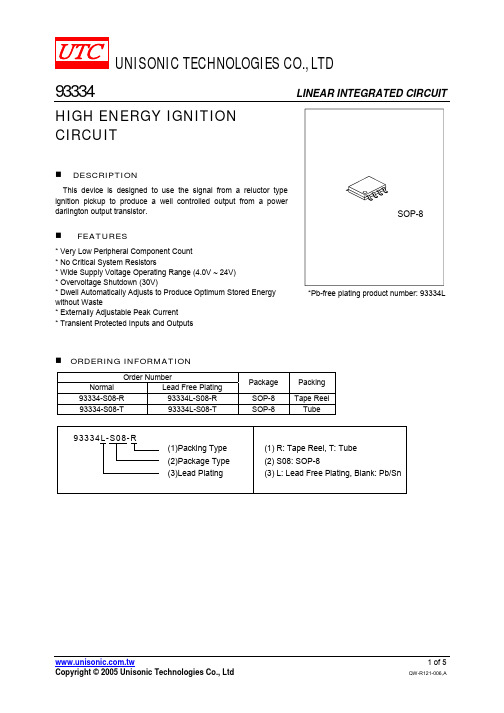
UNISONIC TECHNOLOGIES CO., LTD93334LINEAR INTEGRATED CIRCUITHIGH ENERGY IGNITION CIRCUITDESCRIPTIONThis device is designed to use the signal from a reluctor type ignition pickup to produce a well controlled output from a power darlington output transistor.FEATURES* Very Low Peripheral Component Count * No Critical System Resistors* Wide Supply Voltage Operating Range (4.0V ~ 24V) * Overvoltage Shutdown (30V)* Dwell Automatically Adjusts to Produce Optimum Stored Energy without Waste* Externally Adjustable Peak Current * Transient Protected Inputs and Outputs*Pb-free plating product number: 93334LORDERING INFORMATIONOrder NumberNormal Lead Free PlatingPackage Packing93334-S08-R 93334L-S08-R SOP-8 Tape Reel 93334-S08-T 93334L-S08-T SOP-8 TubePIN CONFIGURATIONOUTC S 2V CCI LSENS GNDPOWER GNDS 1BLOCK DIAGRAM AND TYPICAL APPLICATIONFigure 1ReluctorPickup1.35HComponent ValuesPickup Series resistance = 800Ω±10% @ 25℃, inductance= 1.35H @ 1.0kHz @ 15VrmsCoil Leakage L=0.6mH, primary R=0.43Ω±5% @ 25℃, primary L=7.5mH ~ 8.5mH @ 5.0AR L Load resistor for pickup=10Ω±20%R A, R B Input buffer resistors provide additional transient protection to the already clamped inputs=20k±20%C1, C2For reduction of high frequency noise and spark transients induced in pick-up and leads; optional and non-criticalR BAT Provides load dump protection (but small enough to allow operation at V BAT =4.0V) =300Ω±20% CFilter Transient filter on V CC, non-criticalC DWELL Stores reference, circuit designed for 0.1µF±20%R GAIN R GAIN/R D1 sets the DC gain of the current regulator =5.0k±20%R D2R D2/R D1 set up voltage feedback from R SR S Sense resistor (P D A G in thick film techniques) =0.075Ω±30%R DRIVE Low enough to supply drive to the output Darlington, high enough to keep V CE(SAT) of the I C below Darlington turn-on during load dump = 100Ω±20%, 5.0WR D1Starting with 35Ω assures less than 5.5A, increasing as required to set 5.5A R D1=(I O(PEAK) R S – V REF)/((V REF/R D2)-(1.4/R GAIN))-(≈100Ω)ABSOLUTE MAXIMUM RATINGSPARAMETER SYMBOLRATING UNIT 24Power Supply Voltage-Steady State Transient 300ms or less V CC 90V300 mAOutput Sink Current-Steady State Transient 300ms of less I OUT(SINK)1.0 A1.05 WPower Dissipation Derate above 25°C P D12 mW/°C Junction Temperature T J +125 °C Operating Temperature T OPR -20~+85 °C Storage Temperature T STG -40 ~ 150 °C Note 1. Absolute maximum ratings are those values beyond which the device could be permanently damaged. Absolute maximum ratings are stress ratings only and functional device operation is not implied. 2. The device is guaranteed to meet performance specification within 0 ~+70 operating temperature range and assured by design from -20 ~+85 . ELECTRICAL CHARACTERISTICS (V CC = 13.2V DC , circuit of Figure 3, unless otherwise specified) PARAMETER SYMBOL TEST CONDITIONS MIN TYP MAX UNITV BAT =4.0V DC 3.5 V BAT =8.0V DC 7.2V BAT =12.0V DC 10.4 Internal Supply Voltage, Pin 6 V CC V BAT =14.0V DC11.8VDCV BAT =4.0V DC 3.0 3.4 V BAT =6.0V DC 4.0 5.2V BAT =8.0V DC 4.6 5.3Ignition Coil Current Peak,Cranking RPM 2.0Hz ~ 27HzI PEAK V BAT =10.0V DC 5.15.4 A PEAKF =33Hz 5.1 5.5 F =133Hz 5.1 5.5F =200Hz 4.2 5.4F =267Hz 3.4 4.4 Ignition Coil Current Peak, Normal RPMI PEAK F =333Hz 2.7 3.4 A PEAK F =33Hz 7.5 14.0F =133Hz 5.0 5.9F =200Hz 4.0 4.6F =267Hz 3.0 3.6 Ignition Coil On-Time, Normal RPM RangeT ON F =333Hz 2.3 2.8ms Shutdown VoltageV BAT 25 30 35 V DCTurn-on 360Input Threshold (Static Test) V THR Turn-off 90mV DCInput Threshold Hysteresis V HYS 75 mV DCTurn-on 1.8Input Threshold (Active Operation)V THR Turn-off 1.5 V DCTotal Circuit Lag from ts (Figure 1) until Ignition Coil Current Falls to 10%60 120 µs Ignition Coil Current Fall Time (90% ~ 10%)4.0 µs V BAT =10V DC120V BAT =30V DC280Saturation Voltage IC Output (Pin 7) (R DRIVE = 100Ω)V CE(SAT)V BAT =50V DC540 mV DC Current Limit Reference, Pin 8 V REF120 160 190 mV DCLGNITION COIL CURRENT VERSUS FREQUENCY / PERIOD333I O U T (A )52001331010070152050253330msFrequency, f (Hz)。
3933中文资料

Data Sheet 26301.100†The A3933SEQ is a three-phase MOSFET controller for use with bipolar brushless dc motors. It drives all n-channel external power FETs, allowing system cost savings and minimizing r (DS)on power loss.The high-side drive block is implemented with bootstrap capacitors at each output to provide the floating positive supply for the gate drive.The high-side circuitry also employs a unique “intelligent” FETmonitoring circuit that ensures the gate voltages are at the proper levels before turn-on and during the ON cycle. This device is targeted for applications with motor supplies from 12 V to 28 V.Internal fixed off-time PWM current-control circuitry can be used to regulate the maximum load current to a desired value. The peak load-current limit is set by the user’s selection of an input reference voltage and external sensing resistor. The fixed off-time pulse duration is set by a user-selected external RC timing network.A power-loss braking circuit brakes the motor on an under-voltage condition. The device is configured to either coast or dynamically brake the motor when this occurs.The A3933SEQ is supplied in a 32-lead rectangular (9 x 7) plasticchip carrier (quad pack) for minimum-area, surface-mount applica-tions.3933FEATURES AND BENEFITSI Drives External N-Channel FETs I Intelligent High-Side Gate DriveI Selectable Coast or Dynamic Brake on Power Down I Adjustable Dead Time for Cross-Conduction Protection I Selectable Fast or Slow Current-Decay Modes I Internal PWM Peak Current Control I Reset/Coast InputI 120° Hall Commutation with Internal Pullup I Internal 5-V RegulatorI Low-Side Synchronous Rectification I Direction ControlI PWM Speed-Control Input I Fault-Diagnostic Output IUnder-Voltage ProtectionTHREE-PHASE POWER MOSFET CONTROLLER115 Northeast Cutoff, Box 15036Worcester, Massachusetts 01615-0036 (508) 853-********THREE-PHASE POWER MOSFET CONTROLLERCopyright © 1999, Allegro MicroSystems, Inc.Functional Block DiagramRECOMMENDED OPERATING CONDITIONSSupply Voltage, V BB ...................................... 15 V to 28 Vor, if V BB = V CCOUT ................................... 12 V ±10%Logic Input Voltage Range, V IN .............. -0.3 V to +4.8 V Sense Voltage Range, V SENSE ........................ -1 V to +1 V RC Resistance.......................................... 10 k Ω to 100 k ΩPWM Frequency, f PWM ....................... 20 kHz to 100 kHzLOW-SIDE Dwg. FP-045V 1 OF 3 HIGH-SIDE DRIVERSTO 1 OF 3MOTOR PHASES TO LCAP3933THREE-PHASE POWER MOSFET CONTROLLERELECTRICAL SPECIFICATIONS at T A = 25°C, V BB = V CCOUT = 12 V, C load = 1000 pF, C boot = 0.047 µF (unless noted otherwise).LimitsParameterSymbolConditionsMinTypMaxUnitsSupply CurrentQuiescent Current I BB RESET low, f PWM = 40 kHz –1619mA RESET high–1517mA Reference Voltage V LCAP4.755.0 5.25V Ref. Volt. Load Regulation ∆V LCAP(∆ILCAP)I LCAP = 0 to -2 mA –1025mV Output VoltageV CCOUTV BB = 28 V10.81213.2V Output Voltage Regulation∆V CCOUT(∆ICCOUT)V BB = 28 V, I CCOUT = 0 to -10 mA––25mV Digital Logic LevelsLogic Input Voltage V IH 2.0––V V IL ––0.8V Logic Input CurrentI IH V IH = 2 V –<1.010µA I ILV IL = 0.8 V-70–-130µA Gate DriveLow-Side Output Voltage V GLxH 9.510.511.5V V GLxL I GLx = 1 mA––0.30V High-Side Output Voltage V GHxH 9.010.511.5V V GHxL I GHx = 1 mA ––0.25V Low-Side Output t rGLx 1 V to 8 V –50–ns Switching Time t fGLx 8 V to 1 V –40–ns High-Side Output t rGHx 1 V to 8 V –100–ns Switching Time t fGHx 8 V to 1 V –100–ns DEAD Timet DEADI DEAD = 10 µA –3000–ns (Source OFF to Sink ON)I DEAD = 215 µA –180–nsContinued —NOTES: 1.Typical Data is for design information only.2.Negative current is defined as coming out of (sourcing) the specified device terminal.115 Northeast Cutoff, Box 15036Worcester, Massachusetts 01615-0036 (508) 853-50003933THREE-PHASE POWER MOSFET CONTROLLERELECTRICAL SPECIFICATIONS at T A = 25°C, V BB = V CCOUT = 12 V, C load = 0.001 µF, C boot = 0.047 µF (unless noted otherwise), continued.LimitsParameterSymbolConditions MinTypMaxUnitsBootstrap CapacitorBootstrap Charge Current I Cx 50100150mA Bootstrap Output Voltage V Cx Reference Sx9.510.511.5V Leakage CurrentI Cx High side switched high, Sx = V BB–1520µA Current LimitOffset Voltage V io –0±5.0mV Input bias current I SENSE ––-1.0µA RC Charge Current I RC 8509451040µA RC Voltage Threshold V RCL 1.0 1.1 1.2V V RCH 2.73.0 3.2V PWM frequency Rangef PWM Operating 20–100kHz Protection CircuitryUndervoltage Threshold UVLO Increasing V BB 9.710.210.7V Decreasing V BB 9.35–10.35V Boot-Strap Capacitor Volt.V CxSx V BB = 12 V 9.5––V High-Side Gate-Source Volt.V GHxSx – 6.3–V Fault Output VoltageV FAULT I O = 1 mA––0.8V Brake FunctionBrake Cap. Supply Current I BRKCAP V BB = 8 V, BRKSEL ≥ 2 V –30–µA Low-Side Gate VoltageV GLxHV BB = 0, BRKCAP = 8 V–6.6–VNOTES: 1.Typical Data is for design information only.2.Negative current is defined as coming out of (sourcing) the specified device terminal.3933THREE-PHASE POWER MOSFET CONTROLLERTerminalName1PGND 2RESET 3GLC 4SC 5GHC 6CC 7GLB 8SB 9GHB 10CB 11GLA 12SA 13GHA 14CA 15V CCOUT 16LCAP 17FAULT 18MODE 19V BB 20H121H322H223DIR 24BRAKE 25BRKCAP 26BRKSEL 27PWM 28RC 29SENSE 30REF 31DEAD 32AGNDRESET — A logic input used to enable the device, internally pulled up to V LCAP (+5 V). A logic HIGH will disable the device and force all gate drivers to 0 V, coasting the motor. A logic LOW allows the gate drive to follow commutation logic.This input overrides BRAKE.GLA/GLB/GLC — Low-side, gate-drive outputs for external NMOS drivers. External series-gate resistors (as close aspossible to the NMOS gate) can be used to control the slew rate seen at the power-driver gate, thereby controlling the di/dt and dv/dt of the SA/SB/SC outputs. Each output is designed and specified to drive a 1000 pF load with a rise time of 50 ns.SA/SB/SC — Directly connected to the motor, these terminals sense the voltages switched across the load. These terminals are also connected to the negative side of the bootstrap capaci-tors and are the negative supply connections for the floating high-side drive.GHA/GHB/GHC — High-side, gate-drive outputs for external NMOS drivers. External series-gate resistors (as close aspossible to the NMOS gate) can be used to control the slew rate seen at the power-driver gate, thereby controlling the di/dt and dv/dt of the SA/SB/SC outputs. Each output is designed and specified to drive a 1000 pF load with a rise time of 100 ns.CA/CB/CC — High-side connections for the bootstrap capaci-tors, positive supply for high-side gate drive. The bootstrap capacitor is charged to approximately V CCOUT when theassociated output SA/SB/SC terminal is low. When the output swings high, the voltage on this terminal rises with the output to provide the boosted gate voltage needed for n-channel power FETs.Terminal Descriptionscontinued next page115 Northeast Cutoff, Box 15036Worcester, Massachusetts 01615-0036 (508) 853-50003933THREE-PHASE POWER MOSFET CONTROLLERFAULT — Open-drain output to indicate fault condition; will go active high for any of the following:1 – invalid HALL input code,2 – high-side, gate-source voltage less than 7 V,3 – bootstrap capacitor not sufficiently charged, or4 – under-voltage condition detected at V CCOUT .The fault state for gate-source and bootstrap monitors are cleared at each commutation. If the motor has stalled, then the fault can only be cleared by toggling the RESET terminal or power-up sequence.MODE — A logic input to set current-decay method, internally pulled up to V LCAP (+5 V). When in slow-decay mode (logic HIGH), only the high-side FET is switched open during a PWM OFF cycle. The fast-decay mode (logic LOW) switches both the source and sink FETs.H1/H2/H3 — Hall-sensor inputs; internally pulled up to V LCAP (+5 V). Configured for 120° electrical spacing.DIR — A logic input to reverse rotation, see commutation logic table. Internally pulled up to V LCAP (+5 V).BRAKE — A logic input to short out the motor windings for a braking function. A logic HIGH will turn ON the low-side FETs, turn OFF the high-side FETs. Internally pulled up to V LCAP (+5 V). The braking torque applied will depend on the speed.BRKCAP — Connection for reservoir capacitor. This terminal is used to provide a positive power supply for the sink-drive outputs for a power-down condition. This will allow predict-able braking, if desired. A blocking diode to V CCOUT is re-quired. A 4.7 µF capacitor will provide 6.5 V gate drive for 300 ms. If a power-down braking option is not needed(BRKSEL = LOW) then this terminal should be tied to V CCOUT .BRKSEL — A logic input to enable/disable braking on power-down condition. Internally pulled up to V LCAP (+5 V). If held low, the motor will coast on a power-down condition.PWM — Speed control input, internally pulled up to V LCAP(+5 V). A logic LOW turns OFF all drivers, a logic HIGH will turn ON selected drivers as determined by H1/H2/H3 input logic. Holding the terminal high allows speed/torque control solely by the current-limit circuit via REF analog voltage command.RC — An analog input used to set the fixed off time with an external resistor (R T ) and capacitor (C T ). The t blank time is controlled by the value of the external capacitor (see Applica-tions Information). As a rule, the fixed off time should not be less than 10 µs. The resistor should be in the range of 10 k Ω to 100 k Ω.SENSE — An analog input to the current-limit comparator.A voltage representing load current appears on this terminal during ON time, when it reaches REF voltage, the comparator trips and load current decays for the fixed off-time interval.Voltage transients seen at this terminal when the drivers turn ON are ignored for time t blank .REF — An analog input to the current-limit comparator.Voltage applied here sets the peak load current.I peak = V REF /R S .V CCOUT — A regulated 12 V output; supply for low-side gate drive and bootstrap capacitor charge circuits. It is good practice to connect a decoupling capacitor from this terminal to AGND,as close to the device terminals as possible. The terminal should be shorted to V BB for 12 V applications.V BB — The A3933 supply voltage. It is good practice toconnect a decoupling capacitor from this terminal to AGND, as close to the device terminals as possible. This terminal should be shorted to V CCOUT for 12 V applications.LCAP — Connection for decoupling capacitor for the internal 5 V reference. This terminal can source no more than 2 mA.DEAD — An analog input. A resistor between DEAD and LCAP is selected to adjust turn-off to turn-on time. This delay is needed to prevent shoot-through in the external power FETs.The allowable resistor range is 20 k Ω to 430 k Ω, whichconverts to deadtime of 210 ns to 2.1 µs, using the following equation:t DEAD = (6.75 x 10⁻¹² x R DEAD ) + (75 x 10-9).AGND — The low-level (analog) reference point for the A3933.PGND — The reference point for all low-side gate drivers.Terminal Descriptions (cont’d)3933 THREE-PHASE POWER MOSFET CONTROLLER Commutation Truth TableLogic Inputs Driver OutputsH1H2H3DIR GLA GLB GLC GHA GHB GHC SA SB SCH L H H L L H H L L H Z L H L L H L L H L H L Z H L H H L H H L L L H L L H Z L H L H H L L L L H L Z H L H H H L H L L L H Z L H L L H H L H L H L L H L Z H L H L H L L L L H L Z H H L L L L H L L L H Z L H H H L L L H L H L L H L Z L H L L L L H H L L H Z L L H H L L L H L H L Z H L L L H L H L L L H L L H ZInput LogicMODE PWM RESET Mode OperationL L L Fast decay PWM chop mode, current decayL H L Fast decay Peak current limit, selected drivers ONH L L Slow decay PWM chop mode. current decayH H L Slow decay Peak current limit, selected drivers ONX X H Coast All gate drive outputs OFF, clear fault logicBrake ControlBRAKE BRKSEL Normal Operation Under Voltage or Power Loss ConditionL L Normal run mode Coast, all gate drive outputs OFFL H Normal run mode Dynamic brake, all sink gate drives ONH L Dynamic brake, all sink gate drives ON Coast, all gate drive outputs OFFH H Dynamic brake, all sink gate drives ON Dynamic brake, all sink gate drives ONL = Low Level, H = High Level, X = Don’t Care, Z = High Impedance115 Northeast Cutoff, Box 15036Worcester, Massachusetts 01615-0036 (508) 853-50003933THREE-PHASE POWER MOSFET CONTROLLERApplications Informationbootstrap capacitor. When the bootstrap capacitor has been properly charged, the high side is turned back ON. The circuit will allow three faults of this type within one commutation cycle before signaling a fault and coast the motor (all gate outputs go low).2)Bootstrap Monitor. The bootstrap capacitor is charged whenever a sink-side MOSFET is ON, Sx output goes low, and the load current recirculates. This happens constantly during normal operation. A 60 µs timer is started at the beginning of this cycle and the capacitor is charged with typically 100 mA.The bootstrap capacitor voltage is clamped at approximately 87% of V CCOUT . If the capacitor is not charged to the clamp voltage in 60 µs, a fault is signaled and the motor will coast.3)Undervoltage. The internal V CCOUT regulator supplies the low-side gate driver and the bootstrap charge current. It is critical to ensure that the voltages are at a proper level before enabling any of the outputs. The undervoltage circuit is active during power up and will force a motor coast condition until V CCOUT is greater than approximately 10 V.4)Hall Invalid. Illegal codes for the HALL inputs (000 or 111) will force a fault and coast the motor.Faults are cleared at the beginning of each commutation. If a stalled motor results from a fault, the fault can only be cleared by toggling the RESET terminal or by a power-up sequence.Current Control. Internal fixed off-time PWM circuitry is implemented to limit load current to a desired value. The external sense resistor combined with the applied analog voltage to REF terminal will set the peak current level approximatelyI TRIP ≈ V REF /R S .After the peak level is reached, the sense comparator trips and the load current will decay for a fixed off time.An external resistor (R T ) and capacitor (C T ) are used to set the fixed off-time period (t off = R T x C T ). The t off should be in the range of 10 µs to 50 µs. Longer values for t off can result in audible noise problems.Torque control can be implemented by varying the REF input voltage as long as the PWM input stays high. If direct control of the torque/current is desired by PWM input, a voltage can be applied to the REF input to set an absolute maximum current limit.Bootstrap Capacitor Selection. The high-side bootstrap circuit operates on a charge-transfer principle. The gate charge (Q g ) specification of the external power MOSFET must betaken into consideration. The bootstrap capacitor must be large enough to turn on the MOSFET without losing significant gate voltage. If the bootstrap capacitor is too large, it would take too long to charge up during the off portion of the PWM cycle. The capacitor value must be selected with both of these constraints in mind.1)Minimum bootstrap capacitor value to transfer charge. The charge on the bootstrap capacitor should be 20x greater than the gate charge (Q g ) of the power MOSFET.Example: For Q g = 0.025 µC, selectC boot = 20 x Q g /10.5 V = 0.047 µF.Check for maximum V g drop at turn on: dq = C boot x dV g , where Q g = dq.dV g = dq/C boot = 0.025 µC/0.047 µF = 532 mV.2)Calculate minimum PWM “OFF” cycle with C boot = 0.047 µF.dt = r o x C boot x ln(0.036/[Q g /C boot + 0.036])where r o = 20 ohms, the equivalent internal series resistance of the bootstrap capacitor monitor circuit.The sink-side MOSFET will be held OFF for this minimum time such that the bootstrap capacitor can be recharged independently of the PWM input frequency.The above equation is valid for PWM cycles after the bootstrap capacitor has been charged once. For the first cycle after a motor phase commutates from Hi-Z to GHx ON, or during the first charging cycle at power-up, the circuit will ignore PWM signals until it has been charged.The time required to charge up at power up and at commutation change is approximately:t = C boot x 7 V/0.1 AProtection Circuitry. The A3933 will protect the external MOSFETs by shutting down the gate drive if any of the following conditions are detected:1)Gate Source Monitor (high side only). The voltage on the GHx terminals must stay 7 V higher than the source. If this voltage droops below the threshold, the high side turns OFF,and the low-side gate will turn ON in an attempt to recharge the3933 THREE-PHASE POWER MOSFET CONTROLLER Applications Information (cont’d)PWM Blank. The capacitor (C T) also serves as the means to set the blank time duration. After the off time expires, the selected gates are turned back ON. At this time, large current transients can occur during the reverse recovery time (t rr) of the intrinsic body diodes of the external MOSFETs. To prevent the current-sense comparator from thinking the current spikes are a real overcurrent event, the comparator is blanked:t blank = 1.9 x C T/(1 mA-2/R T)The user must ensure that C T is large enough to cover the current-spike duration.Load Current Recirculation. If MODE has been set for slow decay, the high-side (source) driver will turn OFF forcing the current to recirculate through the pair of sink MOSFETs. If MODE has been selected for fast decay, both the selected high-and low-side gates are turned OFF, which will force the current to recirculate through one sink MOSFET and the high-side clamp diode. Synchronous rectification (only on the low side) allows current to flow through the MOSFET, rather than the clamp diode, during the decay time. This will minimize power loss during the off period. It is important to take into account that, when switching, the intrinsic diodes will conduct during the adjustable deadtime.Braking. The A3933 will dynamically brake by forcing all sink-side MOSFETs ON. This will effectively short out the BEMF. During braking, the load current can be approximated by:I BRAKE = V BEMF/R LPower Loss Brake. The BRKCAP and BRKSEL terminals provide a power-down braking option. By applying a logic level to input BRKSEL, the system can control if the motor is dynamically braked or is allowed to coast during an undervoltage event. The reservoir capacitor on the BRKCAP terminal provides the power to hold the sink-side gates ON after supply voltage is lost. A logic high on BRKSEL will brake the motor, a logic low and it will coast.Layout. Careful consideration must be given to PCB layout when designing high-frequency, fast-switching, high-current circuits.1)The analog ground (AGND), the power ground (PGND), and the high-current return of the external MOSFETs (the negative side of the sense resistor) should return separately to the negative side of the motor supply filtering capacitor. This will minimize the effect of switching noise on the device logic and analog reference.2)Minimize stray inductances by using short, wide copper runs at the drain and source terminals of all power MOSFETs. This includes motor lead connections, the input power buss, and the common source of the low-side power MOSFETs. This will minimize voltages induced by fast switching of large load currents.3)Kelvin connect the SENSE terminal PC trace to the positive side of the sense resistor.115 Northeast Cutoff, Box 15036Worcester, Massachusetts 01615-0036 (508) 853-50003933THREE-PHASE POWER MOSFET CONTROLLERDimensions in Inches(controlling dimensions)Dwg. MA-006-32 in5NOTES: 1. Lead spacing tolerance is non-cumulative.2. Exact body and lead configuration at vendor’s option within limits shown3933THREE-PHASE POWER MOSFET CONTROLLERDimensions in Millimeters(for reference only)Dwg. MA-006-32 mm5201413NOTES: 1. Lead spacing tolerance is non-cumulative.2. Exact body and lead configuration at vendor’s option within limits shownThe products described here are manufactured under one or more U.S.patents or U.S. patents pending.Allegro MicroSystems, Inc. reserves the right to make, from time totime, such departures from the detail specifications as may be required topermit improvements in the performance, reliability, or manufacturabilityof its products. Before placing an order, the user is cautioned to verify thatthe information being relied upon is current.Allegro products are not authorized for use as critical components inlife-support devices or systems without express written approval.The information included herein is believed to be accurate and reliable.However, Allegro MicroSystems, Inc. assumes no responsibility for its use;nor for any infringement of patents or other rights of third parties whichmay result from its use.115 Northeast Cutoff, Box 15036Worcester, Massachusetts 01615-0036 (508) 853-********THREE-PHASE POWER MOSFET CONTROLLERMOTOR DRIVERS FunctionOutput Ratings*Part Number †INTEGRATED CIRCUITS FOR BRUSHLESS DC MOTORS3-Phase Power MOSFET Controller —28 V 39333-Phase Power MOSFET Controller —50 V 39323-Phase Power MOSFET Controller —50 V 76002-Phase Hall-Effect Sensor/Driver 400 mA 26 V 3626Bidirectional 3-Phase Back-EMF Controller/Driver ±600 mA 14 V 89062-Phase Hall-Effect Sensor/Driver 900 mA 14 V 36253-Phase Back-EMF Controller/Driver ±900 mA 14 V 8902–A3-Phase Controller/Drivers ±2.0 A 45 V 2936 & 2936-120INTEGRATED BRIDGE DRIVERS FOR DC AND BIPOLAR STEPPER MOTORSDual Full Bridge with Protection & Diagnostics ±500 mA 30 V 3976PWM Current-Controlled Dual Full Bridge ±650 mA 30 V 3966PWM Current-Controlled Dual Full Bridge ±650 mA 30 V 3968PWM Current-Controlled Dual Full Bridge ±750 mA 45 V 2916PWM Current-Controlled Dual Full Bridge ±750 mA 45 V 2919PWM Current-Controlled Dual Full Bridge ±750 mA 45 V 6219PWM Current-Controlled Dual Full Bridge ±800 mA 33 V 3964PWM Current-Controlled Full Bridge ±1.3 A 50 V 3953PWM Current-Controlled Dual Full Bridge ±1.5 A 45 V 2917PWM Current-Controlled Dual Full Bridge ±1.5 A 45 V 2918PWM Current-Controlled Microstepping Full Bridge ±1.5 A 50 V 3955PWM Current-Controlled Microstepping Full Bridge ±1.5 A 50 V 3957PWM Current-Controlled Dual DMOS Full Bridge ±1.5 A 50 V 3972Dual Full-Bridge Driver ±2.0 A 50 V 2998PWM Current-Controlled Full Bridge ±2.0 A 50 V 3952DMOS Full Bridge PWM Driver ±2.0 A 50 V 3958Dual DMOS Full Bridge ±2.5 A 50 V 3971UNIPOLAR STEPPER MOTOR & OTHER DRIVERSVoice-Coil Motor Driver ±500 mA 6 V 8932–A Voice-Coil Motor Driver ±800 mA 16 V 8958Unipolar Stepper-Motor Quad Drivers 1 A 46 V 7024 & 7029Unipolar Microstepper-Motor Quad Driver 1.2 A 46 V 7042Unipolar Stepper-Motor Translator/Driver 1.25 A 50 V 5804Unipolar Stepper-Motor Quad Driver 1.8 A 50 V 2540Unipolar Stepper-Motor Quad Driver 1.8 A 50 V 2544Unipolar Stepper-Motor Quad Driver 3 A 46 V 7026Unipolar Microstepper-Motor Quad Driver 3 A 46 V 7044*Current is maximum specified test condition, voltage is maximum rating. See specification for sustaining voltage limits or over-current protection voltage limits. Negative current is defined as coming out of (sourcing) the output.†Complete part number includes additional characters to indicate operating temperature range and package style.Also, see 3175, 3177, 3235, and 3275 Hall-effect sensors for use with brushless dc motors.。
XSSA30-U213-V1 开发板数据手册说明书

XSSA30-U213-V1开发板数据手册西安智多晶微电子有限公司XIAN Intelligence Silicon Technology 西安市高新区科技二路72号西安软件园西岳阁102室邮编710075文档修订历史目录1 开发板简介 (3)1.1概述 (4)1.2特点 (4)2 开发板框图 (5)3 开发板引脚分配................................................................................................................................... .63.1时钟引脚............................................................................................................................... .63.2以太网接口........................................................................................................................... .73.3HDMI TX接口 (9)3.4SD卡接口 (11)3.5EEPROM存储芯片 (11)3.6摄像头接口 (11)3.7USB转串口 (13)3.8按键 (14)3.9LED指示灯 (14)3.1040P牛角插座 (14)1.开发板简介1.1 概述:为了更好让客户评估智多晶28nm 30K逻辑FPGA 芯片,我们设计了一款可用于前期评估和移植验证的平台,该开发板的核心器件是西安智多晶的SA5Z-30-D1-8U213,基于低功耗28nm CMOS铜工艺,可用于工业控制、视频接口处理等领域客户的前期评估。
433MHz(315MHz)无线接收芯片中文规格书介绍

产品特征●300MHz到440MHz的频率范围●工作电压:2.2V-3.6V●接受灵敏度高:-108dBm●数据传输速率达10kbps(固定模式)●低功耗⏹315MHz下,最大工作电流2.5mA433MHZ下,最大工作电流3.5mA⏹关闭时的电流为0.9uA⏹扫描操作时(10:1任务周期操作)电流为300uA●唤醒输出标记用来启动解码器和微处理器●天线处的射频辐射非常低●集成度高,外部器件需求少应用领域●汽车远程无钥匙进入(RKE)●远程控制●远程风扇和电灯控制●车库门和门禁控制XC4366是一个ASK/OOK(开关键控)的单晶片射频接收集成电路设备。
它是一个真正的“从天线接收到数据输出”的单片电路。
所有的射频和中频的调谐都在集成电路里完成,这样可以无须手动调整并且降低成本。
实现了一个高度可靠且低成本的解决方案。
XC4366是一个采用16引脚封装且功能齐全的芯片,XC4366A/B/C/DL采用了8引脚封装,功能稍有减少。
XC4366提供了两种附加的功能,(1)一个关闭引脚,在任务周期操作时可以用来关闭设备;(2)一个唤醒输出引脚,当接收到射频信号时,它可以提供一个输出标记。
这些特点使得XC4366可以用在低功耗的应用上,比如RKE和远程控制。
XC4366上提供了所有的中频滤波和数据解调滤波器,所以,不需要外部的滤波器了。
四个解调滤波器的带宽可以由用户从外部控制。
XC4366提供了两种工作模式:固定模式(FIX)和扫描模式(SWP)。
在固定模式中,XC4366用作传统的超外差接收器。
在扫描模式下,XC4366在一个较宽的射频范围内进行扫描。
固定模式提供了更有选择性和针对性的工作模式,并且使得XC4366可以与低成本,精确度较低的发射器一起使用。
1.目录1.目录 (2)2.典型的应用 (3)3.订货须知 (4)4.引脚框图 (4)5.引脚的选择性 (5)6.引脚定义 (5)7.极限最大值(注释1) (6)8工作额定值(注释2) (6)9.电气特性 (7)10.功能框图 (9)11.应用说明和功能描述 (9)12.设计步骤 (9)12.1步骤1:选择工作模式 (10)12.2步骤2:选择参考晶振 (10)12.3步骤3.选择CTH电容 (12)12.4步骤4:选择CAGC电容 (13)12.5步骤5:选择解调器的带宽 (14)13.其他应用程序信息 (15)13.1天线阻抗匹配 (15)13.2关机功能 (17)13.3电源旁路电容 (18)13.4可选带通滤波器可增加选择性 (18)13.5数据噪声控制 (18)13.6唤醒功能 (19)14.封装信息 (20)14.1 16引脚的SOP封装 (20)14.2 8引脚的SOP封装 (21)14.3 16引脚的SOP顶层标志 (21)14.4 8引脚的SOP顶层标志 (22)2.典型的应用315MHz 800bps的开关键控接收器433.92MHz 800bps的开关键控接收器3.订货须知4.引脚框图标准的16引脚或者8引脚的封装5.引脚的选择性标准的16引脚允许完整的可配置型的控制。
X9315WMIZ-2.7T1中文资料
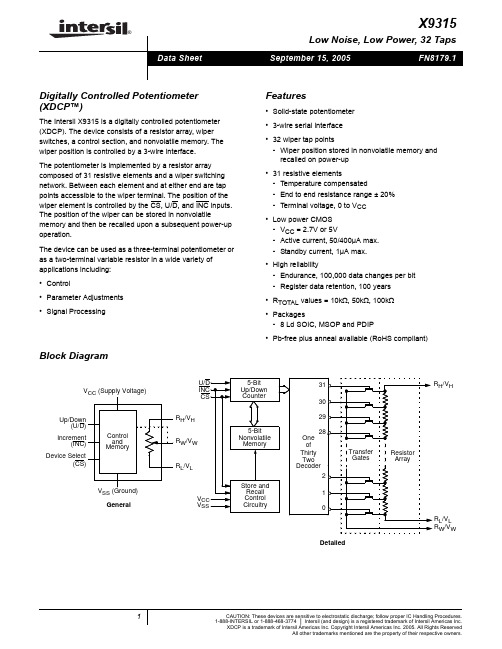
®X9315Low Noise, Low Power, 32 TapsDigitally Controlled Potentiometer (XDCP™)The Intersil X9315 is a digitally controlled potentiometer (XDCP). The device consists of a resistor array, wiper switches, a control section, and nonvolatile memory. The wiper position is controlled by a 3-wire interface.The potentiometer is implemented by a resistor array composed of 31 resistive elements and a wiper switching network. Between each element and at either end are tap points accessible to the wiper terminal. The position of the wiper element is controlled by the CS, U/D, and INC inputs. The position of the wiper can be stored in nonvolatilememory and then be recalled upon a subsequent power-up operation.The device can be used as a three-terminal potentiometer or as a two-terminal variable resistor in a wide variety of applications including:•Control•Parameter Adjustments •Signal ProcessingFeatures•Solid-state potentiometer •3-wire serial interface•32 wiper tap points-Wiper position stored in nonvolatile memory and recalled on power-up •31 resistive elements-Temperature compensated-End to end resistance range ± 20% -Terminal voltage, 0 to V CC •Low power CMOS -V CC = 2.7V or 5V-Active current, 50/400µA max.-Standby current, 1µA max.•High reliability-Endurance, 100,000 data changes per bit -Register data retention, 100 years •R TOTAL values = 10k Ω, 50k Ω, 100k Ω•Packages-8 Ld SOIC, MSOP and PDIP•Pb-free plus anneal available (RoHS compliant)Block DiagramH /V HL /V L W /V WUp/Down(U/D)Increment(INC)(CS)V (Supply Voltage)SS R H /V HR W /V R L /V LGeneralDetailedOrdering InformationPART NUMBER PART MARKING V CC LIMITS(V)R TOTAL(kΩ)TEMP RANGE(°C)PACKAGEX9315WM*AAW 5 ±10% 100 to 708 Ld MSOPX9315WMZ* (Note)DDT0 to 708 Ld MSOP (Pb-free) X9315WMI*AAX-40 to 858 Ld MSOPX9315WMIZ* (Note)AKW-40 to 858 Ld MSOP (Pb-free) X9315WP X9315WP0 to 708 Ld PDIPX9315WPI X9315WP I-40 to 858 Ld PDIPX9315WS*X9315W0 to 708 Ld SOICX9315WSZ* (Note)X9315W Z0 to 708 Ld SOIC (Pb-free) X9315WSI*X9315W I-40 to 858 Ld SOICX9315WSIZ* (Note)X9315W Z I-40 to 858 Ld SOIC (Pb-free) X9315UM*500 to 708 Ld MSOPX9315UMZ* (Note)DDS0 to 708 Ld MSOP (Pb-free) X9315UMI*AEB-40 to 858 Ld MSOPX9315UMIZ* (Note)DDR-40 to 858 Ld MSOP (Pb-free) X9315UP X9315UP0 to 708 Ld PDIPX9315UPI X9315UP I-40 to 858 Ld PDIPX9315US*X9315U0 to 708 Ld SOICX9315USZ* (Note)X9315U Z0 to 708 Ld SOIC (Pb-free) X9315USI*X9315U I-40 to 858 Ld SOICX9315USIZ* (Note)X9315U Z I-40 to 858 Ld SOIC (Pb-free) X9315TM*AEJ1000 to 708 Ld MSOPX9315TMZ* (Note)DDN0 to 708 Ld MSOP (Pb-free) X9315TMI*ADZ-40 to 858 Ld MSOPX9315TMIZ* (Note)DDL-40 to 858 Ld MSOP (Pb-free) X9315TP X9315TP0 to 708 Ld PDIPX9315TPI X9315TP I-40 to 858 Ld PDIPX9315TS*X9315T0 to 708 Ld SOICX9315TSZ* (Note)X9315T Z0 to 708 Ld SOIC (Pb-free) X9315TSI*X9315T I-40 to 858 Ld SOICX9315TSIZ* (Note)X9315T Z I-40 to 858 Ld SOIC (Pb-free)X9315TP-2.7X9315TP F 2.7-5.5100 to 708 Ld PDIP X9315TPI-2.7X9315TP G -40 to 858 Ld PDIP X9315WM-2.7*AAU 0 to 708 Ld MSOPX9315WMZ-2.7* (Note)AOI 0 to 708 Ld MSOP (Pb-free)X9315WMI-2.7*AAV-40 to 858 Ld MSOPX9315WMIZ-2.7* (Note)-40 to 858 Ld MSOP (Pb-free)X9315WP-2.7X9315WP F 0 to 708 Ld PDIP X9315WPI-2.7X9315WP G -40 to 858 Ld PDIP X9315WS-2.7*X9315W F 0 to 708 Ld SOICX9315WSZ-2.7* (Note)X9315W Z F 0 to 708 Ld SOIC (Pb-free)X9315WSI-2.7*X9315W G -40 to 858 Ld SOICX9315WSIZ-2.7* (Note)X9315W Z G -40 to 858 Ld SOIC (Pb-free)X9315UM-2.7*AEK 500 to 708 Ld MSOPX9315UMZ-2.7* (Note)AKU 0 to 708 Ld MSOP (Pb-free)X9315UMI-2.7*AEA -40 to 858 Ld MSOPX9315UMIZ-2.7* (Note)AJG-40 to 858 Ld MSOP (Pb-free)X9315UP-2.70 to 708 Ld PDIP X9315UPI-2.7-40 to 858 Ld PDIP X9315US-2.7*X9315U F 0 to 708 Ld SOICX9315USZ-2.7* (Note)X9315U Z F 0 to 708 Ld SOIC (Pb-free)X9315USI-2.7*X9315U G -40 to 858 Ld SOICX9315USIZ-2.7* (Note)X9315U Z G -40 to 858 Ld SOIC (Pb-free)X9315TM-2.7*AEI 1000 to 708 Ld MSOPX9315TMZ-2.7* (Note)DDP 0 to 708 Ld MSOP (Pb-free)X9315TMI-2.7*ADY -40 to 858 Ld MSOPX9315TMIZ-2.7* (Note)DDM -40 to 858 Ld MSOP (Pb-free)X9315TS-2.7*X9315T F 0 to 708 Ld SOICX9315TSZ-2.7* (Note)X9315T Z F 0 to 708 Ld SOIC (Pb-free)X9315TSI-2.7*X9315T G -40 to 858 Ld SOICX9315TSIZ-2.7* (Note)X9315T Z G-40 to 858 Ld SOIC (Pb-free)NOTE:Intersil Pb-free plus anneal products employ special Pb-free material sets; molding compounds/die attach materials and 100% matte tin plate termination finish, which are RoHS compliant and compatible with both SnPb and Pb-free soldering operations. Intersil Pb-free products are MSL classified at Pb-free peak reflow temperatures that meet or exceed the Pb-free requirements of IPC/JEDEC J STD-020.*Add "T1" suffix for tape and reel.Ordering Information (Continued)PART NUMBERPART MARKING V CC LIMITS(V)R TOTAL (k Ω)TEMP RANGE(°C)PACKAGEPin DescriptionsR H /V H and R L /V LThe high (R H /V H ) and low (R L /V L ) terminals of the X9315 are equivalent to the fixed terminals of a mechanical potentiometer. The minimum voltage is V SS and the maximum is V CC . The terminology of R L /V L and R H /V H references the relative position of the terminal in relation to wiper movement direction selected by the U/D input, and not the voltage potential on the terminal.R W /V WR W /V w is the wiper terminal and is equivalent to the movable terminal of a mechanical potentiometer. The position of the wiper within the array is determined by the control inputs. The wiper terminal series resistance is typically 200Ω at V CC = 5V.Up/Down (U/D)The U/D input controls the direction of the wiper movement and whether the counter is incremented or decremented.Increment (INC)The INC input is negative-edge triggered. Toggling INC will move the wiper and either increment or decrement the counter in the direction indicated by the logic level on the U/D input.Chip Select (CS)The device is selected when the CS input is LOW. The current counter value is stored in nonvolatile memory when CS is returned HIGH while the INC input is also HIGH. After the store operation is complete the X9315 will be placed in the low power standby mode until the device is selected once again.Pin ConfigurationPrinciples of OperationThere are three sections of the X9315: the input control, counter and decode section; the nonvolatile memory; and the resistor array. The input control section operates just like an up/down counter. The output of this counter is decoded to turn on a single electronic switch connecting a point on the resistor array to the wiper output. Under the proper conditions the contents of the counter can be stored innonvolatile memory and retained for future use. The resistor array is comprised of 31 individual resistors connected in series. At either end of the array and between each resistor is an electronic switch that transfers the connection at that point to the wiper.The wiper, when at either fixed terminal, acts like itsmechanical equivalent and does not move beyond the last position. That is, the counter does not wrap around when clocked to either extreme.The electronic switches on the device operate in a “make before break” mode when the wiper changes tap positions. If the wiper is moved several positions, multiple taps are connected to the wiper for t IW (INC to V W change). The R TOTAL value for the device can temporarily be reduced by a significant amount if the wiper is moved several positions.When the device is powered-down, the last wiper position stored will be maintained in the nonvolatile memory. When power is restored, the contents of the memory are recalled and the wiper is set to the value last stored.Instructions and ProgrammingThe INC, U/D and CS inputs control the movement of the wiper along the resistor array. With CS set LOW the device is selected and enabled to respond to the U/D and INC inputs. HIGH to LOW transitions on INC will increment or decrement (depending on the state of the U/D input) a five bit counter. The output of this counter is decoded to select one of thirty two wiper positions along the resistive array.The value of the counter is stored in nonvolatile memory whenever CS transitions HIGH while the INC input is also HIGH.The system may select the X9315, move the wiper and deselect the device without having to store the latest wiper position in nonvolatile memory. After the wiper movement is performed as described above and once the new position is reached, the system must keep INC LOW while taking CS HIGH. The new wiper position will be maintained untilPin NamesSYMBOL DESCRIPTION R H /V H High terminal R W /V W Wiper terminal R L /V L Low terminal V SS Ground V CC Supply voltage U/DUp/Down control inputV CC CS INC U/D R H /V H V SS12348765X9315DIP/SOIC/MSOPR L /V L R W /V WINC Increment control input CSChip Select control inputPin NamesSYMBOL DESCRIPTIONchanged by the system or until a power-up/down cycle recalled the previously stored data.This procedure allows the system to always power-up to a preset value stored in nonvolatile memory; then during system operation minor adjustments could be made. The adjustments might be based on user preference, system parameter changes due to temperature drift, etc...The state of U/D may be changed while CS remains LOW. This allows the host system to enable the device and then move the wiper up and down until the proper trim is attained.Symbol TableMode SelectionCS INCU/D MODEL H Wiper Up LL Wiper Down HX Store Wiper Position HX X Standby CurrentL XNo Store, Return to StandbyWAVEFORMINPUTS OUTPUTS Must be steady Will be steady May change from Lo w to High Will change from Lo w to High May change from High to Low Will change from High to Low Don’t Care:Changes Allowed Changing:State Not Known N/ACenter Line is High ImpedanceNotes:(1) Absolute linearity is utilized to determine actual wiper voltage versus expected voltage = (V w(n)(actual) - V w(n)(expected)) = ±1 MlMaximum.(2) Relative linearity is a measure of the error in step size between taps = R W(n+1) - [R w(n) + Ml] = ±0.2 Ml.(3) 1 Ml = Minimum Increment = R TOT /31.(4) Typical values are for T A = 25°C and nominal supply voltage.(5) This parameter is periodically sampled and not 100% testedAbsolute Maximum RatingsRecommended Operating ConditionsTemperature under bias. . . . . . . . . . . . . . . . . . . . . .-65°C to +135°C Storage temperature . . . . . . . . . . . . . . . . . . . . . . . .-65°C to +150°C Voltage on CS, INC, U/D, V H , V L andV CC with respect to V SS . . . . . . . . . . . . . . . . . . . . . . . -1V to +7V ∆V = |V H –V L |. . . . . . . . . . . . . . . . . . . . . . . . . . . . . . . . . . . . . . . . .5V Lead temperature (soldering 10 seconds). . . . . . . . . . . . . . . .300°C I W (10 seconds). . . . . . . . . . . . . . . . . . . . . . . . . . . . . . . . . . .±7.5mATemperature (Commercial) . . . . . . . . . . . . . . . . . . . . . 0°C to +70°C Temperature (Industrial). . . . . . . . . . . . . . . . . . . . . . .-40°C to +85°C Supply Voltage (V CC ) (Note 4) LimitsX9315. . . . . . . . . . . . . . . . . . . . . . . . . . . . . . . . . . . . . . . 5V ± 10%X9315-2.7. . . . . . . . . . . . . . . . . . . . . . . . . . . . . . . . . .2.7V to 5.5VCAUTION: Stresses above those listed under “Absolute Maximum Ratings” may cause permanent damage to the device. This is a stress rating only; the functional operation of the device (at these or any other conditions above those listed in the operational sections of this specification) is not implied. Exposure to absolute maximum rating conditions for extended periods may affect device reliability.Potentiometer Characteristics(Over recommended operating conditions unless otherwise stated.)SYMBOLPARAMETERTEST CONDITIONS/NOTES LIMITSMIN TYP MAX.UNIT End to end resistance tolerance±20%V VH V H terminal voltage 0V CC V V VLV L terminal voltage 0V CC V Power ratingR TOTAL ≥ 10k Ω10mW R W Wiper resistance I W = 1mA, V CC = 5V 200400ΩR W Wiper resistance I W = 1mA, V CC = 2.7V4001000ΩI WWiper current ±3.75mA Noise Ref: 1kHz -120dBV Resolution3%Absolute linearity (1)V w(n)(actual) - V w(n)(expected)±1MI (3)Relative linearity (2)V w(n + 1) - [V w(n) + MI ]±0.2MI (3)R TOTAL temperature coefficient ±300ppm/°CRatiometric temperature coefficient±20ppm/°C C H /C L /C WPotentiometer capacitancesSee circuit #310/10/25pFDC Electrical Specifications(Over recommended operating conditions unless otherwise specified.SYMBOL PARAMETERTEST CONDITIONSLIMITSUNIT MINTYP (4)MAX I CC1V CC active current (Increment)CS = V IL , U/D = V IL or V IH and INC = 0.4V @ max. t CYC50µA I CC2V CC active current (Store) (EEPROM Store)CS = V IH , U/D = V IL or V IH and INC = V IH @ max. t WR 400µA I SB Standby supply currentCS = V CC - 0.3V, U/D and INC = V SS orV CC - 0.3V 1µA I LI CS, INC, U/D input leakage current V IN = V SS to V CC±10µA V IH CS, INC, U/D input HIGH voltage V CC x 0.7V CC + 0.5V V IL CS, INC, U/D input LOW voltage -0.5V CC x 0.1V C IN (5)CS, INC, U/D input capacitanceV CC = 5V, V IN = V SS , T A =25°C, f = 1MHz10pFEndurance and Data RetentionPARAMETER MIN UNITMinimum endurance 100,000Data changes per bitData retention100YearsTest Circuit #1Test Circuit #2Circuit #3 SPICE Macro ModelTest Point V W /R WV H /R HV L /R LV SForceCurrentV L VWTest PointV H /R HV W /R W V L /R LC HC L R W10pF10pFR HR LR TOTALC W 25pFAC Conditions of TestInput pulse levels 0V to 3V Input rise and fall times 10ns Input reference levels1.5VAC Electrical Specifications(Over recommended operating conditions unless otherwise specified)SYMBOLPARAMETERLIMITSUNIT MIN TYP (6)MAXt Cl CS to INC setup 100ns t lD INC HIGH to U/D change 100ns t DI U/D to INC setup 2.9µs t lL INC LOW period 1µs t lH INC HIGH period1µs t lC INC Inactive to CS inactive 1µs t CPH CS Deselect time (NO STORE)100ns t CPH CS Deselect time (STORE)10ms t IW INC to Vw change 15µs t CYC INC cycle time4µs t R , t F (7)INC input rise and fall time500µs t PU (7)Power-up to wiper stable 5µs t R V CC (7)V CC power-up rate 0.250V/ms t WRStore cycle510msPower-up and Down RequirementsThere are no restrictions on the power-up or power-down conditions of V CC and the voltages applied to the potentiometer pins provided that V CC is always morepositive than or equal to V H , V L , and V W , i.e., V CC ≥ V H , V L , V W . The V CC ramp rate spec is always in effect.AC TimingNotes:(6)Typical values are for T A = 25°C and nominal supply voltage.(7)This parameter is not 100% tested.(8)MI in the A.C. timing diagram refers to the minimum incremental change in the V W output due to a change in the wiper position.Performance Characteristics (Typical)Typical NoiseCSINCU/DV Wt CIt IL t IH t CYCt IDDIt IWMI(8)t ICt CPHt Ft R10%90%90%(Store)0-10-20-30-40-50-60-70-80-90-100-110-120-130-140-150102030405060708090100Frequency (kHz)N o i s e (d B )110120130140150160170180190200Typical Rtotal vs. TemperatureTypical Total Resistance Temperature CoefficientTypical Wiper Resistance10000 9800960094009200900088008600840082008000R t o t a l-55-45-35-25-15-5515253545556575Temperature8595105115125C°-55-350-300-250-200-150-100-50-45-35-25-15-55152535TemperaturePPM455565758595105115125°C0100200300400R w (Ω)500600700800246810121416Tap1820222426283032V CC = 2.7VTypical Absolute% Error per Tap PositionTypical Relative% Error per Tap PositionApplications InformationElectronic digitally controlled (XDCP) potentiometers provide three powerful application advantages; (1) the variability and reliability of a solid-state potentiometer, (2) the flexibility of computer-based digital controls, and (3) the retentivity of nonvolatile memory used for the storage of multiple potentiometer settings or data.40.0%30.0%20.0%10.0%0.0%-10.0%-20.0%-30.0%-40.0%3691215TapA b s o l u t e % E r r o r182124273020.0%15.0%10.0%5.0%0.0%-5.0%-10.0%-15.0%-20.0%3691215R e l a t i v e % E r r o r1821242730TapBasic Configurations of Electronic PotentiometersBasic CircuitsV R V W /R WV RIThree terminal potentiometer;variable voltage dividerTwo terminal variable resistor;variable currentV HV LCascading Techniques Buffered Reference Voltage –++5VR 1+V-5V V WV REFV OUTOP-07R W /V WR W /V W+V+V+VX(a)(b)V OUT = V W /R WNoninverting Amplifier+–V SV OR 2R 1V O = (1 + R 2/R 1)V SLM308AVoltage Regulator R 1R 2I adjV O (REG) = 1.25V (1 + R 2/R 1) + I adj R 2V O (REG)V IN317Comparator with HysteresisV UL = {R 1/(R 1 + R 2)} V O (max)V LL = {R 1/(R 1 + R 2)} V O (min)+–V SV OR 2R 1}}LT311A+5V-5V(for additional circuits see AN115)0.118 ± 0.002(3.00 ± 0.05)0.040 ± 0.002(1.02 ± 0.05)0.150 (3.81)Ref.0.193 (4.90)0.030 (0.76)0.036 (0.91)0.032 (0.81)0.007 (0.18)0.005 (0.13)0.008 (0.20)0.004 (0.10)0.0216 (0.55)7° Typ.R 0.014 (0.36)0.118 ± 0.002(3.00 ± 0.05)0.012 + 0.006 / -0.002(0.30 + 0.15 / -0.05)0.0256 (0.65) Typ.8-Lead Miniature Small Outline Gull Wing Package Type MNOTE:1.ALL DIMENSIONS IN INCHES AND (MILLIMETERS)Ref.NOTE:1.ALL DIMENSIONS IN INCHES (IN PARENTHESES IN MILLIMETERS)2.PACKAGE DIMENSIONS EXCLUDE MOLDING FLASH0.020 (0.51)0.016 (0.41)0.150 (3.81)0.125 (3.18)0.110 (2.79)0.090 (2.29)0.430 (10.92)0.360 (9.14)0.300(7.62) Ref.Pin 1 Index0.145 (3.68)0.128 (3.25)0.025 (0.64)0.015 (0.38)Pin 1Seating 0.065 (1.65)0.045 (1.14)0.260 (6.60)0.240 (6.10)0.060 (1.52)0.020 (0.51)Typ. 0.010 (0.25)0°15°8-Lead Plastic Dual In-Line Package Type PHalf Shoulder Width On All End Pins Optional.073 (1.84)Max.0.325 (8.25)0.300 (7.62)PlaneAll Intersil U.S. products are manufactured, assembled and tested utilizing ISO9000 quality systems.Intersil Corporation’s quality certifications can be viewed at /design/qualityIntersil products are sold by description only. Intersil Corporation reserves the right to make changes in circuit design, software and/or specifications at any time without notice. Accordingly, the reader is cautioned to verify that data sheets are current before placing orders. Information furnished by Intersil is believed to be accurate and reliable. However, no responsibility is assumed by Intersil or its subsidiaries for its use; nor for any infringements of patents or other rights of third parties which may result from its use. No license is granted by implication or otherwise under any patent or patent rights of Intersil or its subsidiaries.For information regarding Intersil Corporation and its products, see 0.150 (3.80)0.158 (4.00)0.228 (5.80)0.244 (6.20)0.014 (0.35)0.019 (0.49)Pin 1Pin 1 Index0.010 (0.25)0.020 (0.50)0.050 (1.27)0.188 (4.78)0.197 (5.00)0.004 (0.19)0.010 (0.25)0.053 (1.35)0.069 (1.75)(4X) 7°0.016 (0.410)0.037 (0.937)0.0075 (0.19)0.010 (0.25)0° - 8°X 45°8-Lead Plastic Small Outline Gull Wing Package Type SNOTE: ALL DIMENSIONS IN INCHES (IN PARENTHESES IN MILLIMETERS)。
三星 BX1931N BX2031 BX2031N BX2231 BX2331说明书

SyncMaster BX1931N/BX2031/BX2031N/BX2231/BX2331/BX2431显示器用户手册颜色和外观可能根据产品的不同而有所变化,并且出于性能提高对规格进行的更改,恕不另行通知。
目录主要安全注意事项使用前注意事项 . . . . . . . . . . . . . . . . . . . . . . . . . . . . . . . . . . . . . . . . . . . . 1-1保管和维护 . . . . . . . . . . . . . . . . . . . . . . . . . . . . . . . . . . . . . . . . . . . . . . . . 1-2安全注意事项 . . . . . . . . . . . . . . . . . . . . . . . . . . . . . . . . . . . . . . . . . . . . . . 1-3安装产品包装清单 . . . . . . . . . . . . . . . . . . . . . . . . . . . . . . . . . . . . . . . . . . . . . . . . . . 2-1安装支架 . . . . . . . . . . . . . . . . . . . . . . . . . . . . . . . . . . . . . . . . . . . . . . . . . . 2-2连接 PC . . . . . . . . . . . . . . . . . . . . . . . . . . . . . . . . . . . . . . . . . . . . . . . . . . 2-3使用 HDMI 缆线进行连接 . . . . . . . . . . . . . . . . . . . . . . . . . . . . . . . . . . . . . 2-4Kensington 防盗锁 . . . . . . . . . . . . . . . . . . . . . . . . . . . . . . . . . . . . . . . . . 2-5使用本产品设置最佳分辨率. . . . . . . . . . . . . . . . . . . . . . . . . . . . . . . . . . . . . . . . . . . . 3-1标准信号模式表 . . . . . . . . . . . . . . . . . . . . . . . . . . . . . . . . . . . . . . . . . . . . 3-2标准信号模式表 . . . . . . . . . . . . . . . . . . . . . . . . . . . . . . . . . . . . . . . . . . . . 3-3标准信号模式表 . . . . . . . . . . . . . . . . . . . . . . . . . . . . . . . . . . . . . . . . . . . . 3-4标准信号模式表 . . . . . . . . . . . . . . . . . . . . . . . . . . . . . . . . . . . . . . . . . . . . 3-5标准信号模式表 . . . . . . . . . . . . . . . . . . . . . . . . . . . . . . . . . . . . . . . . . . . . 3-6标准信号模式表 . . . . . . . . . . . . . . . . . . . . . . . . . . . . . . . . . . . . . . . . . . . . 3-7安装设备驱动程序 . . . . . . . . . . . . . . . . . . . . . . . . . . . . . . . . . . . . . . . . . . . 3-8产品操作按钮 . . . . . . . . . . . . . . . . . . . . . . . . . . . . . . . . . . . . . . . . . . . . . . 3-9使用屏幕调整菜单(OSD:屏幕菜单) . . . . . . . . . . . . . . . . . . . . . . . . . 3-10安装软件Natural Color . . . . . . . . . . . . . . . . . . . . . . . . . . . . . . . . . . . . . . . . . . . . . . 4-1MagicTune . . . . . . . . . . . . . . . . . . . . . . . . . . . . . . . . . . . . . . . . . . . . . . . . 4-2MultiScreen . . . . . . . . . . . . . . . . . . . . . . . . . . . . . . . . . . . . . . . . . . . . . . . 4-3故障排除显示器自诊断 . . . . . . . . . . . . . . . . . . . . . . . . . . . . . . . . . . . . . . . . . . . . . . 5-1常见故障检查 . . . . . . . . . . . . . . . . . . . . . . . . . . . . . . . . . . . . . . . . . . . . . . 5-2常见问题解答 . . . . . . . . . . . . . . . . . . . . . . . . . . . . . . . . . . . . . . . . . . . . . . 5-3更多信息规格 . . . . . . . . . . . . . . . . . . . . . . . . . . . . . . . . . . . . . . . . . . . . . . . . . . . . . 6-1省电功能 . . . . . . . . . . . . . . . . . . . . . . . . . . . . . . . . . . . . . . . . . . . . . . . . . . 6-2规格 . . . . . . . . . . . . . . . . . . . . . . . . . . . . . . . . . . . . . . . . . . . . . . . . . . . . . 6-3省电功能 . . . . . . . . . . . . . . . . . . . . . . . . . . . . . . . . . . . . . . . . . . . . . . . . . . 6-4规格 . . . . . . . . . . . . . . . . . . . . . . . . . . . . . . . . . . . . . . . . . . . . . . . . . . . . . 6-5省电功能 . . . . . . . . . . . . . . . . . . . . . . . . . . . . . . . . . . . . . . . . . . . . . . . . . . 6-6规格 . . . . . . . . . . . . . . . . . . . . . . . . . . . . . . . . . . . . . . . . . . . . . . . . . . . . . 6-7省电功能 . . . . . . . . . . . . . . . . . . . . . . . . . . . . . . . . . . . . . . . . . . . . . . . . . . 6-8规格 . . . . . . . . . . . . . . . . . . . . . . . . . . . . . . . . . . . . . . . . . . . . . . . . . . . . . 6-9省电功能 . . . . . . . . . . . . . . . . . . . . . . . . . . . . . . . . . . . . . . . . . . . . . . . . . 6-10规格 . . . . . . . . . . . . . . . . . . . . . . . . . . . . . . . . . . . . . . . . . . . . . . . . . . . . 6-11省电功能 . . . . . . . . . . . . . . . . . . . . . . . . . . . . . . . . . . . . . . . . . . . . . . . . . 6-12 ROHS . . . . . . . . . . . . . . . . . . . . . . . . . . . . . . . . . . . . . . . . . . . . . . . . . . . 6-13三星全球服务网 . . . . . . . . . . . . . . . . . . . . . . . . . . . . . . . . . . . . . . . . . . . 6-141主要安全注意事项1-1使用前注意事项本手册所用图标使用本手册•使用本产品前请仔细阅读安全注意事项。
数控电位器X9319中文资料

数控电位器X9319X D C P T M一概述11描述Xicor公司的X9319 为数控电位器XDCP该器件包含一个电阻阵列滑动开关一个控制段和非易失性存储器滑动端位置由一个三线接口控制电位器由包含99个电阻单元的电阻阵列和一个滑动开关网络组成在每个电阻单元的两端之间有抽头点可访问滑动终端滑动端的位置由CS U/D和INC输入端控制滑动端的位置可存储在非易失性存储器中在上电的操作中可重新被调用该器件可用作一个三终端的电位器以控制电压或用作一个两终端的可变电阻以控制电流其应用范围非常广泛1 2 特点z固态电位器z三线串行接口z端点电压0V到+10Vz100个滑动抽头点-滑动端的位置存储在非易失性存储器中在上电操作中重新调用z99个电阻单元-温度补偿-点对点电阻范围+ 20%z低功耗CMOS-V CC=5V-工作电流 3m A(最大值)-待机电流 1mA最大值z高可靠性-每位可允许100000次数据擦写-寄存器数据保存期为100年z总电阻值R=10K和50KTOTALz封装-8引脚 SOIC和DIP13应用范围z液晶显示器偏压控制z直流偏压调整z增益和偏移调整z激光二极管偏压控制z电压稳压器输出控制1 4 方框图1 5 引脚配置及说明1引脚配置图2引脚名称控制脚引脚为低时脚可使滑动端上升或下降降引脚降输入脚控制滑动端移动的方向器件被选定为高时4引脚详述z R H 和R LX9319的高端RH和低端R L等效于机械电位器的一个固定端R H 和R L这两个术语只是规定了滑动端的相对位置而滑动端的滑动方向由U/D输入脚选择z R WR W是滑动端等效于机械电位器的可移动端滑动端在电阻阵列中的位置由控制输入脚决定滑动端电阻值通常为40z升/降输入脚 (U/D)升/降输入脚控制滑动端移动的方向以及控制计数器是增加或是减少z增加输入脚INC增加输入脚是负边沿触发触发INC将使滑动端向计数器增加或减少的方向移动移动的方向由U/D 端输入的逻辑电平决定z片选输入脚CS当CS输入脚为低时器件被选中当CS变为高且INC输入端也为高时当前计数器的值被储存在非易失性存储器中当储存操作完成后X9319将处于低功耗的等待方式直到器件再次被选中1 6 订购信息订购号RTOTAL封装工作温度范围X9319WS810k8引脚SOIC0°C至70°CX9319WS8I10k8引脚SOIC–40°C至+85°CX9319WP810k8引脚塑料DIP0°C至70°CX9319WP8I10k8引脚塑料DIP–40°C至+85°CX9319US850k8引脚SOIC0°C至70°CX9319US8I50k8引脚SOIC–40°C至+85°CX9319UP850k8引脚塑料DIP0°C至70°CX9319UP8I50k8引脚塑料DIP–40°C至+85°C二特性2 1 极限参数*工作温度–65°C至+135°C 贮存温度–65°C至+150°C CS INC U/D和V CC的电压相对于V SS–1V至+7V R H R W R L的电压相对于地+12V 引线温度焊接10秒300°C10秒+6mAI*注强度超出所列的极限参数可能导致器件的永久性损坏这些仅仅是极限参数并不意味着在极限条件下或在任何其它超出推荐工作条件所示参数的情况下器件能有效工作延长在极限参数条件下的工作时间会影响器件的可靠性2 2 电位器特性(V CC= 5V ±10%, T A= 工作温度范围内除非另有规定)2 3 直流工作特性(V CC= 5V ±10%, T A= 工作温度范围内除非另有规定)2 4 可擦写次数和数据保存期(V CC= 5V ±10%, T A= 工作温度范围内除非另有规定)参数最小单位最小擦写次数100000每位数据变化数据保存期100年注1绝对线性用于确定滑动端的实际电压与期望电压之差= [V(R)–V(R W(n)(期望))]/MIV(R W(n)(期望)) =W(n)(实际)n(V(R H)-V(R L))/99 + V(R L)其中 n =0至992相对线性用于测量抽头间步距的差= [V(R W(n+1))–(V(R W(n)) – MI)]/MI3 1 Ml =最小增量= [V(R H)–V(R L)]/994典型值是T A= 25°C 且在额定电源电压下的值5由器件特性保证6比例Ratiometric温度系数= (V(R W)T1(n)–V(R W)T2(n))/[V(R W)T1(n)(T1–T2) x 106]其中T1和T2为2 种温度并且n =0至997以抽头位置为31的滑动端测量R L接地使用测试电路2 5 测试的交流条件输入脉冲电平0.8V至2.0V输入上升和下降时间10ns输入参考电平 1.4V测试电路等效电路2 6 交流工作特性(V CC= 5V ±10%, T A= 工作温度范围内除非另有规定)27上电和掉电要求脚上电时或上电前将CS和INC拉高在该时序完为避免不必要的抽头位置改变或意外存储在VCC达到其最终值1毫秒以后数字电位器的数据手成后必须对电位器上电在上电过程中要等到VCC斜率规格总是有效册参数才能完全适用VCC28 交流时序三工作原理3 1 X9319的三个组成部分控制部分非易失性存储器以及电阻阵列控制部分的工作就像一个升/降计数器这个计数器的输出被译码而接通一个单接点的电子开关以便把电阻阵列上的一个点连接到滑动输出端计数器的内容可以存储在非易失性存储器中并保持以便今后使用电阻阵列包含99个独立串联的电阻在电阻阵列的二个端点以及每个电阻之间都有一个电子开关可将该点与滑动端引脚R相连W滑动端就像等效的机械滑动端一样不会移动到超出第一个或末端位置即当计数器达到一个极端时不会循环当滑动端改变抽头位置时器件的电子开关以先接通后断开的方式工作若滑动端移动了几个时间INC到V W变化内连接到滑动端而且器件的R TOTAL值要暂时减少某位置多个抽头即会在tIW一个值当器件被断电最后存储的滑动端位置将被维持在非易失性存储器中电源恢复时存储器中的内容被调用因而滑动端被设置到上一次储存的值3 2 指令和程序INC U/D和CS三个输入端控制滑动端沿着电阻阵列移动只有CS置低器件被才能选中才能对U/D和INC输入端作出响应在INC输入端由高至低的变化将增加或减少这取决于U/D输入端的状态一个7位计数器的值这个计数器的输出被译码进行一百选一的操作使滑动端的位置沿电阻阵列移动只要当CS跳变到为高且INC输入脚也为高时计数器的值即被存储在非易失性存储器中系统可能选中X9319移动滑动端而后又中断选择该器件且并未将最终的滑动端位置储存在非易失性存储器中在滑动端依上述过程移动后一旦达到新的位置系统必须保持INC为低而CS为高则新的滑动端位置将被保持直到被系统改变或一次掉电后再上电周期重新调用以前存储的数据这个程序将允许系统在每次上电时预置一个值储存在非易失性存储器中因而当系统工作时只要进行很小的调整这种调整可以是基于用户的选择由于温度漂移引起的系统参数变化等当CS保持为低时U/D的状态可以被改变这就允许主系统使能器件然后移动滑动端上升或下降直到达到适合的微调为止3 3 模式选择四应用资料电子数控电位器XDCP具备三个有力应用优势1固态电位器的可变性和可靠性2基于计算机数控的灵活性3用于存储多个电位器设置或数据的非易失性存储器的保持性能良好电位器的基本配置三终端电位器可变分压器两终端可变电阻可变电流基本电路图缓冲基准电压串联技艺单电源反相放大器稳压器偏移电压调整具有滞后作用的比较器五封装信息18引脚塑料小型封装S型8引脚SOIC注所有尺寸均以英寸为单位括号中的以毫米为单位28引脚塑料DIP封装条码P8注1所有尺寸均以英寸为单位括号中的以毫米为单位2封装尺寸不包括模型的薄膜声明本资料仅供参考如有不同之处请以英文资料为准。
Eaton Wheelock Exceder LED3低频声光报警器系列产品说明说明书

DescriptionEaton has developed the Wheelock Exceder LED3 Low Frequency Sounder Strobes (LFHSK3/LFHSH3) and Sounders (LFHNK3) tomeet the National Fire Protection Association (NFPA) low frequency sounder requirements for sleeping rooms - NFPA 72 for fire alarm and NFPA 720 for Carbon Monoxide (CO) alarm. In a single device, the Exceder LED Low Frequency Sounders can provide alarm signals for dual applications - T3 (Fire) and T4 (CO) tones. Eaton offers low frequency sounder strobe models for both low and high candela settings, ideal for retrofits and new construction.The Exceder LED3 Low Frequency Sounder Strobes and Sounders feature multiple 520 Hz modes of operation: T3 (fire), T4 (CO), Continuous, T3/T4 Sync Control.Like the entire Wheelock Exceder LED3 product line, the Low Frequency Sounder Strobes feature an advanced power saving LED technology in a sleek, modern, single-gang enclosure that will provide high energy efficiency and an aesthetically pleasing low profile design that will blend with the building‘s interior décor. LFHSK3 strobe models include a 110 candela setting, and LFHSH3 strobe models include a 177 candela setting.Providing a sleek aesthetic appearance, the Exceder LFHSK3/LFHSH3 and LFHNK3 models feature one of the industry’s smallest footprints and a sleek, modern, low-profile design. Installers will benefit from its comprehensive feature list, multiple 520 Hz modes of operation, lowest current draw, no tools needed for setting changes, and convenient mounting options. The LFTP trim plate, which is included in all LFHNK3/LFHSK3/LFHSH3 models, allows for ease of installation for retrofit projects that have single-gang backboxes installed. These products are suitable for indoor wall-mount applications. The Sounder and Sounder Strobe models are for 24V operation.Eaton’s Exceder LED3 strobes meet the 20 millisecond light pulse duration requirements of the 2016 edition of NFPA 72. By meeting this latest requirement, xenon and LED devices can now be in the same field of view. With the Exceder LED3 line, Eaton now offers a full range of products with low and high candela settings ideal for both retrofits and new construction.The Exceder LED3 Low Frequency Sounders and Sounder Strobes are UL Listed for indoor use under Standard 1971 and 464 and ULC under S525 and S526.In addition, the Wheelock Exceder LED3 product line has been UL/ULC listed as compatible with all Fire Alarm Control Panels (FACP) and accessories that have been determined to be compatible with Wheelock RSS strobe-based products including the RSS, CH, E, EH, ET , ST , HS, MT , S8, SA, STH and Z Series. The listing alsoincludes the ability to install the Exceder LED3 strobes in the same notification zone and field of view with any Wheelock RSS strobe models.Exceder LED3 Low FrequencySounder Strobes and Sounders2EATON Features•Meets dual low frequency sounder codes for sleeping rooms in a single device• NFPA 72 for fire alarm•NFPA 720 for CO alarm•4 Settings in 1 device • T3 (fire)• T4 (CO)• Continuous (Coded)•T3/T4•Energy efficient• Patented LED technology provides industry’s lowest current draw •Low-profile design• Smallest footprint with sleek, modern aesthetics • 110 or 177 candela setting (dependent on model)•Easy-to-install• Finger slide switches--No tools needed for setting changes• Built-in level adjustment feature and snap-on grille cover •IN/OUT screw terminals using #12 to #18 AWG wires•Mounting Options: Trim plate (LFTP) for single-gang backbox included in all LFHNK3/LFHSK3/LFHSH3 models; Exceder LSPKBB backboxes and 4” square backboxes•Strobe synchronization components• Meet synchronizing standards with Wheelock’s DSM Sync Modules or Power Supplies •Compliance• NFPA 72 2016 - 20 ms flash duration requirements• UL 1971, UL 464, ULC S525, ULC S526• California State Fire Marshal (CSFM) - Pending for LFHSH3• ADA/NFPA/ANSI/OSHA •RoHSNote:N Please read these specifications and associated installationinstructions, before using, specifying, or installing this product. Visit /massnotification for current installation instructions.G eneral Notes•Strobes are designed to flash at 1 flash per second minimum over their “Regulated Voltage Range.” Note that NFPA-72 specifies a flash rate of 1 to 2 flashes per second and ADA Guidelines specify a flash rate of 1 to 3 flashes per second.•All candela ratings represent minimum effective Strobe intensity based on UL 1971.SettingsThe 520 tone is generated within the appliance itself. When the selector switch is set for T3 or T4, the sound pattern is also generated within the appliance. When the selection switch is set to continuous, the product is listed for coded operations. The T3/T4 pattern or other pattern must be generated by the FACP according to the alarm condition sensed by the panel (fire or CO alarm).When the device is set to T3/T4, the appliance can switch from T3 to T4 based upon the condition sensed by the FACP and passed to the Wheelock DSM module.DrawingsFigure 1. Wall Low Frequency Sounder StrobeFigure 2. Wall Low Frequency Sounder Exceder LED3 Sounders UL/ULC Max Current a24VDC ModelHorn Settings16.0-33.0LFHNK3Continuous Code 3Code 4Code 3/Code 40.0980.0980.0980.098T able 2. Horn Only Current DrawExceder LED3 Sounder Strobes UL/ULC Max Current a24VDC ModelsHorn Setting16-33 Volts 110 cd177 cdLFHSK3/LFHSH3Continuous Code 3Code 4Code 3/Code 40.2900.2900.290 0.2900.3440.3440.3440.344Table 1. Horn Strobe Current Draw3EATON T able 5. Specification & Ordering InformationModelStrobe CandelaRedWhiteLetteringSync w/ DSM orWheelock Power SuppliesSounder Strobes LFHSKR3LFHSKW3 LFHSKR3-AL LFHSKW3-AL LFHSKR3-CO LFHSKW3-CO LFHSKR3-N LFHSKW3-N LFHSHR3LFHSHW3 LFHSHR3-AL LFHSHW3-AL LFHSHR3-CO LFHSHW3-CO LFHSHR3-N LFHSHW3-N 110 110 110 110 110 110110110 177177177177177177177177X X X X X X X XX X X X X X X XFIRE FIRE ALERT ALERT CO CONo Lettering No Lettering FIRE FIRE ALERT ALERT CO CONo Lettering No Lettering X X X X X X X X X X X X X X X XSounders LFHNKR3LFHNKW3LFHNKR3-AL LFHNKW3-AL LFHNKR3-CO LFHNKW3-CO LFHNKR3-N LFHNKW3-N X X X XX X X XFIRE FIRE ALERT ALERT CO CONo Lettering No LetteringX X X X X X X XAccessoriesDescriptionRedWhiteLSPKBB-R LSPKBB-W07560757Exceder LED Backbox Exceder LED BackboxXXT able 6. Specifications Physical Material Red or white textured UV stabilized, colored impregnated engineered plastic. Exceeds 94V-0 UL flammability rating Weight 1.10 lbs.LensLight Emitting Diode (LED) in a rugged Lexan lens Dimensions6.23”H x 4.69” W x 1.77” D (with LFTP trim plate)Operating TemperatureIndoor: 32°F to 122°F (0°C to 50°C) and maximum humidity of 93%Mounting & Wire Connections Mounting (indoor only)Wall-mount applications for sounder strobe (LFHSK3/LFHSH3); Wall and ceiling-mount applications for the sounder only model (LFHNK3). Trim plate for single-gang backbox included in all LFHNK3/LFHSK3/LFHSH3 models; Exceder LSPKBB backboxes and 4” square backboxes Wire Connections #12 through #18 AWGPower & General Operating voltage 24 VDC: 16 - 33 VDCStrobe Output Rating UL 1971: 110 candela output (LFHSK3 models)/ 177 candela output (LFHSH3 models)Strobe Flash RateStrobes are designed to flash at 1 flash per secondSynchronization Models Strobes can be synchronized with Wheelock’s DSM Sync Modules, PS Power Supplies, using Wheelock patented sync protocolTemporal Audible PatternContinuous, Code 3, Code 4 or Code 3/Code 4 Sync Control. The Code 3 temporal pattern (1/2 second on, 1/2 second off, 1/2 second on, 1/2 second off, 1/2 second on, 1-1/2 off and repeat) is specified by ANSI and NFPA 72 for standard emergency evacuation signaling. The Code 4 temporal pattern (four cycles of 100 milliseconds ± 10 percent “on” and 100 milliseconds ± 10 percent “off,” followed by 5 seconds ± 10 percent “off)is specified by NFPA 720.a RMS current ratings are per UL maximum RMS method. UL max current rating is the maximum RMS current within the listed voltage range (16-33v). For strobesthe UL max current is usually at the minimum listed voltage. For audibles the max current is usually at the maximum listed voltage. For unfiltered FWR ratings, see installation instructions.LFHSK3/LFHSH3/LFHNK3 24V Reverberant dBA per UL 464Description16.0V24.0V33.0VContinuous Code 3Code 4 bCode 3/Code 4 b 808080808080808080808080T able 3. Sound Output (SPL) - ULLFHSK3/LFHSH3/LFHNK3 dBA per ULC S525-16cDescription16.0V24.0V33.0VContinuous Code 3Code 4Code 3/Code 4808080808080808080808080T able 4. Sound Output (SPL) - ULCEaton is a registered trademark.All other trademarks are property of their respective owners.Eaton1000 Eaton Boulevard Cleveland, OH 44122United States EatonLife safety & mass notification solutions 273 Branchport Ave.Long Branch, NJ /massnotification © 2018 EatonAll Rights Reserved Printed in USAPublication No. TD450121EN May 2018Architects and Engineers SpecificationsThe low frequency sounders and sounder strobes appliances shall be Wheelock ® Exceder™ LED3 series LFHNK3 Sounder for wall- and ceiling-mount applications and LFHSK3/LFHSH3 Sounder Strobe for wall-mount applications with a low-profile design or approved equals. The sounders shall be UL Listed under UL 464 for Fire Protective Service and ULC S525. Sounders equipped with strobes shall be listed under UL 1971 for Emergency Devices for the Hearing-Impaired and ULC S526. The Series shall be Restriction of Hazardous Substances (RoHS) compliant and contain no mercury or other hazardous substances. In addition, the sounder strobes shall meet the requirements of FCC Part 15 and ICES-003. All inputs shall be compatible with standard reverse polarity supervision of circuit wiring by a Fire Alarm Control Panel (FACP) with the ability to operate from 16 to 33 VDC.The LFHSK3/LFHSH3 Sounder Strobe shall produce a flash rate of one (1) flash per second over the Regulated Voltage Range and shall incorporate a Light Emitting Diode (LED) as the light source with a rugged Lexan® lens. The strobe shall be of low current design. The LED strobe flash duration shall be 20 ms. The strobe intensity of LFHSK3 models shall have a 110 candela, and the LFHSH3 models shall have a 177 candela.The audible shall have a minimum of four (4) 520 Hz modes of operation: T3 (fire), T4 (CO), Continuous, T3/T4 Sync Control.The LFHSK3, LFHSH3 and LFHNK3 shall be designed for indoor surface or flush mounting. Mounting options shall include LEDspeaker backboxes and to standard 4” square backboxes and single-gang backboxes with LFTP trim plate. The sounder and sounder strobe shall incorporate a mounting plate with a snap-on grille cover and shall mount to standard electrical hardware requiring no additional trimplate or adapter. Removal of an appliance shall result in a supervision fault condition by the Fire Alarm Control Panel (FACP). All notification appliances shall be backwards compatible.The LFHNK3, LFHSK3, and LFHSH3 wall models, which shall include the LFTP trimplate, shall have a low profile measuring 6.23” H x 4.69” W x 1.77” D. Finish shall be red or white. Special lettering, ALERT , CO and No lettering, shall be available.When synchronization is required, the appliance shall be compatible with Wheelock’s DSM Sync Modules, PS Power Supplies, or other manufacturer’s panels with built-in Wheelock Patented Sync Protocol. The strobes shall not drift out of synchro-nization at any time during operation. If the sync protocol fails to operate, the strobe shall revert to a non-synchronized flash-rate and still maintain (1) flash per second over its Regulated Voltage Range. The appliance shall also be designed so that the audible signal may be silenced while maintaining strobe activation when used with Wheelock patented sync protocol.UL 1971, UL 464, ULC S525, ULC S526, CSFM, FCC, RoHS, ICESNote:N Due to continuous development of our products, specifications and offerings are subject to change without notice in accordance with Cooper Wheelock Inc., dba Eaton standard terms and conditions.WE ENCOURAGE AND SUPPORT NICET CERTIFICATION3 YEAR WARRANTY。
- 1、下载文档前请自行甄别文档内容的完整性,平台不提供额外的编辑、内容补充、找答案等附加服务。
- 2、"仅部分预览"的文档,不可在线预览部分如存在完整性等问题,可反馈申请退款(可完整预览的文档不适用该条件!)。
- 3、如文档侵犯您的权益,请联系客服反馈,我们会尽快为您处理(人工客服工作时间:9:00-18:30)。
-40 to +85
8 Ld MSOP (Pb-free)
M8.118
X9313ZP-3
X9313ZP D
VCC RANGE (V)
4.5 to 5.5
3 to 5.5
X9313UMI-3* X9313UMIZ-3* (Note) X9313US-3*, ** X9313USZ-3*, ** (Note) X9313WM-3* X9313WMZ-3* (Note) X9313WMI-3*
13UE 13UEZ X9313U D X9313U ZD 13WD DDG 13WE
• 31 resistive elements - Temperature compensated - End to end resistance range ±20% - Terminal voltages, -VCC to +VCC
• Low power CMOS - VCC = 3V or 5V - Active current, 3mA max. - Standby current, 500µA max.
The device can be used as a three-terminal potentiometer or as a -terminal variable resistor in a wide variety of applications including:
• Control
• Parameter adjustments
The Intersil X9313 is a digitally controlled potentiometer (XDCP). The device consists of a resistor array, wiper switches, a control section, and nonvolatile memory. The wiper position is controlled by a 3-wire interface.
8 Ld PDIP*** (Pb-free) MDP0031
8 Ld PDIP
MDP0031
8 Ld PDIP*** (Pb-free) MDP0031
8 Ld SOIC
MDP0027
8 Ld SOIC (Pb-free)
M8.15
8 Ld SOIC
MDP0027
8 Ld SOIC (Pb-free)
RTOTAL (kΩ) 50 10
1
50 10
TEMPERATURE RANGE (°C) -40 to +85 -40 to +85 0 to +70 0 to +70 0 to +70 -40 to +85 -40 to +85 0 to +70 -40 to +85 -40 to +85 0 to +70 -40 to +85 -40 to +85 -40 to +85 0 to +70 0 to +70 -40 to +85 -40 to +85 0 to +70 0 to +70 -40 to +85 -40 to +85 0 to +70 -40 to +85 -40 to +85 0 to +70 0 to +70 -40 to +85 -40 to +85 0 to +70 0 to +70
DEVICE SELECT (CS)
CONTROL AND
MEMORY
VSS (GROUND) GENERAL
RH/VH RW/VW RL/VL
VCC VSS
5-BIT NONVOLATILE
MEMORY
STORE AND RECALL CONTROL
CIRCUITRY
29
28 ONE OF THIRTY-TWO OUTPUTS ACTIVE
• High reliability - Endurance, 100,000 data changes per bit - Register data retention, 100 years
• RTOTAL values = 1kΩ, 10kΩ, 50kΩ • Packages
- 8 Ld SOIC, 8 Ld MSOP and 8 Ld PDIP
• Pb-free plus anneal available (RoHS compliant)
Block Diagram
VCC (SUPPLY VOLTAGE)
DECODER
U/D
5-BIT
INC
UP/DOWN
31
CS
COUNTER
30
RH/VH
UP/DOWN (U/D)
INCREMENT (INC)
3 to 5.5
1
0 to +70
8 Ld MSOP
M8.118
X9313ZMZ-3* (Note)
DDK
0 to +70
8 Ld MSOP (Pb-free)
M8.118
X9313ZMI-3*
13ZE
-40 to +85
8 Ld MSOP
M8.118
X9313ZMIZ-3* (Note)
13ZEZ
-40 to +85 -40 to +85 0 to +70 0 to +70 0 to +70 0 to +70 -40 to +85
PACKAGE
PKG. DWG. #
8 Ld MSOP
M8.118
8 Ld MSOP (Pb-free)
M8.118
8 Ld PDIP
MDP0031
8 Ld SOIC
The potentiometer is implemented by a resistor array composed of 31 resistive elements and a wiper switching network. Between each element and at either end are tap points accessible to the wiper terminal. The position of the wiper element is controlled by the CS, U/D, and INC inputs. The position of the wiper can be stored in nonvolatile memory and then be recalled upon a subsequent power-up operation.
MDP0027
8 Ld SOIC (Pb-free)
M8.15
8 Ld SOIC
MDP0027
8 Ld SOIC (Pb-free)
M8.15
8 Ld MSOP (Pb-free)
M8.118
8 Ld MSOP
M8.118
8 Ld MSOP (Pb-free)
M8.118
8 Ld PDIP
MDP0031
元器件交易网
®
Data Sheet
X9313
Digitally Controlled Potentiometer (XDCP™)
April 18, 2007
FN8177.5
Linear, 32 Taps, 3 Wire Interface, Terminal Voltages ± VCC
All other trademarks mentioned are the property of their respective owners.
元器件交易网
X9313
Ordering Information
PART NUMBER X9313UMI X9313UMIZ (Note) X9313UP X9313US* X9313USZ* (Note) X9313USI X9313USIZ (Note) X9313WMZ (Note) X9313WMI* X9313WMIZ* (Note) X9313WP X9313WPZ-3 X9313WPI X9313WPIZ X9313WS*, ** X9313WSZ*, ** (Note) X9313WSI* X9313WSIZ* (Note) X9313ZM X9313ZMZ (Note) X9313ZMI*, ** X9313ZMIZ*, ** (Note) X9313ZP X9313ZPI X9313ZPIZ (Note) X9313ZS*, ** X9313ZSZ*, ** (Note) X9313ZSI* X9313ZSIZ* (Note) X9313UM-3T1 X9313UMZ-3T1 (Note)
1-888-INTERSIL or 1-888-468-3774 | Intersil (and design) is a registered trademark of Intersil Americas Inc.
XDCP is a trademark of Intersil Americas Inc. Copyright Intersil Americas Inc. 2005, 2006, 2007. All Rights Reserved
M8.118
8 Ld MSOP (Pb-free)
M8.118
8 Ld SOIC
MDP0027
8 Ld SOIC (Pb-free)
M8.15
8 Ld MSOP
M8.118