MAX6125ESA中文资料
MEMORY存储芯片MAX1483ESA1中文规格书

For pricing, delivery, and ordering information, please contact /Dallas Direct! at1-888-629-4642, or visit Maxim’s website at _______________General Description The MAX1482 and MAX1483 are low-power trans-ceivers for RS-485 and RS-422 communication. Both feature slew-rate-limited drivers that minimize EMI and reduce reflections caused by improperly terminated cables. Data rates are guaranteed up to 250kbps.The MAX1482/MAX1483 draw only 20µA of supply cur-rent. Additionally, they have a low-current shutdown mode that consumes only 0.1µA. Both parts operatefrom a single +5V supply.Drivers are short-circuit current limited and are protect-ed against excessive power dissipation by thermal shutdown circuitry that places the driver outputs into a high-impedance state. The receiver input has a fail-safefeature that guarantees a logic-high output if the input is open circuit.The MAX1482 is full duplex and the MAX1483 is half duplex. Both parts have a 1⁄8-unit-load input impedancethat guarantees up to 256 transceivers on the bus.________________________Applications Low-Power RS-485/RS-422 Networks Transceivers for EMI-Sensitive Applications Industrial-Control Local Area Networks Large 256-Node LANs ____________________________Features ♦Low 20µA Operating Current♦Slew-Rate Limited for Reduced EMI and Reduced Reflections♦0.1µA Low-Current Shutdown Mode♦Designed for RS-485 and RS-422 Applications ♦Operate from a Single +5V Supply♦-7V to +12V Common-Mode Input Voltage Range ♦Allows up to 256 Transceivers on the Bus—Guaranteed (1⁄8-unit load)♦Current Limiting and Thermal Shutdown for Driver Overload ProtectionMAX1482/MAX1483________________________________________________________________ Integrated Products 1_________________Pin Configurations_________Typical Operating Circuits Ordering Information µMAX is a registered trademark of Integrated products, Inc.找MEMORY 、二三极管上美光存储M A X 1482/M A X 1483Line Length vs. Data Rate The RS-485/RS-422 standard covers line lengths up to 4000 feet. For line lengths greater than 4000 feet, see Figure 16.Figure 13 shows the system differential voltage for the parts driving 4000 feet of 26AWG twisted-pair wire at 110kHz into 120Ωloads. Even after 4000 feet of cable,the MAX1482/MAX1483 output shows virtually no dis-tortion.Typical Applications The MAX1482/MAX1483 transceivers are designed forbidirectional data communications on multipoint bus transmission lines. Figures 14 and 15 show typical net-work applications circuits. These parts can also be used as line repeaters, with cable lengths longer than 4000 feet, as shown in Figure 16.To minimize reflections, the line should be terminated at both ends in its characteristic impedance, and stub lengths off the main line should be kept as short as possible (although the slew-rate-limited MAX1482 and MAX1483 are more tolerant of imperfect termination than standard RS-485 ICs).Isolated RS-485For isolated RS-485 applications, see the MAX253 and MAX1480 data sheets.20µA, 1⁄8-Unit-Load, Slew-Rate-Limited RS-485 Transceivers 10______________________________________________________________________________________Figure 14. MAX1483 Typical Half-Duplex RS-485 NetworkR O DI RECEIVER INPUTV Y -V Z 2µs/div 5010-150Figure 13. System Differential Voltage at 250kbps (125kHz)Driving 4000 Feet of Cable。
MAX6126BASA30中文资料

19-2647; Rev 4; 7/04
Ultra-High-Precision, Ultra-Low-Noise, Series Voltage Reference
General Description
The MAX6126 is an ultra-low-noise, high-precision, lowdropout voltage reference. This family of voltage references feature curvature-correction circuitry and high-stability, laser-trimmed, thin-film resistors that result in 3ppm/°C (max) temperature coefficients and an excellent ±0.02% (max) initial accuracy. The proprietary low-noise reference architecture produces a low flicker noise of 1.3µVP-P and wideband noise as low as 60nV/√Hz (2.048V output) without the increased supply current usually found in low-noise references. Improve wideband noise to 35nV/ √ Hz and AC power-supply rejection by adding a 0.1µF capacitor at the noise reduction pin. The MAX6126 series mode reference operates from a wide 2.7V to 12.6V supply voltage range and load-regulation specifications are guaranteed to be less than 0.025Ω for sink and source currents up to 10mA. These devices are available over the automotive temperature range of -40°C to +125°C. The MAX6126 typically draws 380µA of supply current and is available in 2.048V, 2.500V, 3.000V, 4.096V, and 5.000V output voltages. These devices also feature dropout voltages as low as 200mV. Unlike conventional shunt-mode (two-terminal) references that waste supply current and require an external resistor, the MAX6126 offers supply current that is virtually independent of supply voltage and does not require an external resistor. The MAX6126 is stable with 0.1µF to 10µF of load capacitance. The MAX6126 is available in the tiny 8-pin µMAX, as well as 8-pin SO packages.
MEMORY存储芯片MAX1487ESA+中文规格书

2Maxim Integrated Supply Voltage (V CC ) (12V)Control Input Voltage (RE , DE)...................-0.5V to (V CC + 0.5V)Driver Input Voltage (DI).............................-0.5V to (V CC + 0.5V)Driver Output Voltage (A, B)...................................-8V to +12.5VReceiver Input Voltage (A, B).................................-8V to +12.5VReceiver Output Voltage (RO)....................-0.5V to (V CC + 0.5V)Continuous Power Dissipation (T A = +70°C)8-Pin Plastic DIP (derate 9.09mW/°C above +70°C)....727mW14-Pin Plastic DIP (derate 10.00mW/°C above +70°C)..800mW8-Pin SO (derate 5.88mW/°C above +70°C).................471mW 14-Pin SO (derate 8.33mW/°C above +70°C)...............667mW 8-Pin µMAX (derate 4.1mW/°C above +70°C)..............830mW 8-Pin CERDIP (derate 8.00mW/°C above +70°C).........640mW 14-Pin CERDIP (derate 9.09mW/°C above +70°C).......727mW Operating Temperature Ranges MAX4_ _C_ _/MAX1487C_ A...............................0°C to +70°C MAX4__E_ _/MAX1487E_ A.............................-40°C to +85°C MAX4__M_/MAX1487MJA.............................-55°C to +125°C Storage Temperature Range.............................-65°C to +160°C Lead Temperature (soldering, 10sec).............................+300°C DC ELECTRICAL CHARACTERISTICS(V CC = 5V ±5%, T A = T MIN to T MAX , unless otherwise noted.) (Notes 1, 2)Stresses beyond those listed under “Absolute Maximum Ratings” may cause permanent damage to the device. These are stress ratings only, and functional operation of the device at these or any other conditions beyond those indicated in the operational sections of the specifications is not implied. Exposure to absolute maximum rating conditions for extended periods may affect device reliability.VV IN = -7V V IN = 12V V IN = -7V V IN = 12V Input Current (A, B)I IN2V TH k Ω48-7V ≤V CM ≤12V, MAX487/MAX1487R INReceiver Input Resistance -7V ≤V CM ≤12V, all devices exceptMAX487/MAX1487R = 27Ω(RS-485), Figure 40.4V ≤V O ≤2.4VR = 50Ω(RS-422)I O = 4mA, V ID = -200mV I O = -4mA, V ID = 200mV V CM = 0V -7V ≤V CM ≤12V DE, DI, REDE, DI, RE MAX487/MAX1487,DE = 0V, V CC = 0V or 5.25VDE, DI, RE R = 27Ωor 50Ω, Figure 4R = 27Ωor 50Ω, Figure 4R = 27Ωor 50Ω, Figure 4DE = 0V;V CC = 0V or 5.25V,all devices exceptMAX487/MAX1487CONDITIONS k Ω12µA ±1I OZR Three-State (high impedance)Output Current at Receiver V 0.4V OL Receiver Output Low Voltage3.5V OH Receiver Output High VoltagemV 70ΔV TH Receiver Input HysteresisV -0.20.2Receiver Differential ThresholdVoltage-0.2mA 0.25mA -0.81.01.55V OD2Differential Driver Output(with load)V 2V 5V OD1Differential Driver Output (no load)µA ±2I IN1Input Current V 0.8V IL Input Low VoltageV 2.0V IH Input High VoltageV 0.2ΔV OD Change in Magnitude of DriverCommon-Mode Output Voltagefor Complementary Output StatesV 0.2ΔV OD Change in Magnitude of DriverDifferential Output Voltage forComplementary Output StatesV 3V OC Driver Common-Mode OutputVoltageUNITS MIN TYP MAX SYMBOL PARAMETER找MEMORY 、二三极管上美光存储Low-Power, Slew-Rate-Limited RS-485/RS-422 Transceivers12Maxim Integrated MAX481/MAX483/MAX485/MAX487–MAX491/MAX1487500mV/div 20ns/div ABRO 2V/divV CC = 5V T A = +25°C 500mV/div 20ns/divAB RO2V/divV CC = 5V T A = +25°C500mV/div 400ns/div ABRO2V/div V CC = 5V T A = +25°C 500mV/div 400ns/divA B RO2V/div V CC = 5VT A = +25°CFigure 14. Receiver Propagation Delay Test CircuitFigure 15. MAX481/MAX485/MAX490/MAX491/MAX1487Receiver t PHL Figure 16. MAX481/MAX485/MAX490/MAX491/MAX1487Receiver t PLHPHL Figure 18. MAX483, MAX487–MAX489 Receiver t PLH。
MEMORY存储芯片MAX4172ESA+T中文规格书

General DescriptionThe MAX4172 is a low-cost, precision, high-side current-sense amplifier for portable PCs, telephones, and othersystems where battery/DC power-line monitoring is critical.High-side power-line monitoring is especially useful inbattery-powered systems, since it does not interfere withthe battery charger’s ground path. Wide bandwidth andground-sensing capability make the device suitable forclosed-loop battery-charger and general-purpose current-source applications. The 0 to 32V input common-moderange is independent of the supply voltage, which ensuresthat current-sense feedback remains viable, even whenconnected to a battery in deep discharge.T o provide a high level of flexibility, the MAX4172 functionswith an external sense resistor to set the range of loadcurrent to be monitored. It has a current output that canbe converted to a ground-referred voltage with a singleresistor, accommodating a wide range of battery voltagesand currents.An open-collector power-good output (PG ) indicateswhen the supply voltage reaches an adequate levelto guarantee proper operation of the current-senseamplifier. The MAX4172 operates with a 3.0V to 32Vsupply voltage, and is available in a space-saving, 8-pinμMAX ® or SO package.Applications●Portable PCs: Notebooks/Subnotebooks/Palmtops●Battery-Powered/Portable Equipment●Closed-Loop Battery Chargers/Current Sources●Smart-Battery Packs●Portable/Cellular Phones●Portable Test/Measurement Systems●Energy Management SystemsBenefits and Features ●Ideal for High-Side Monitoring •3V to 32V Supply Operation •±0.5% Typical Full-Scale Accuracy Over T emperature •High Accuracy +2V to +32V Common-Mode Range, Functional Down to 0V, Independent of Supply Voltage •800kHz Bandwidth [V SENSE = 100mV (1C)]•200kHz Bandwidth [V SENSE = 6.25mV (C/16)]●Minimizes Board Space Requirements •μMAX and SO Packages μMAX is a registered trademark of Maxim Integrated Products, Inc.+Denotes a lead(Pb)-free/RoHS-compliant package.PART TEMP RANGE PIN-PACKAGE MAX4172ESA+-40°C to +85°C 8 SO MAX4172EUA+-40°C to +85°C 8 μMAX MAX4172GUA+-40°C to +105°C 8 µMAXMAX4172Low-Cost, Precision, High-Side Current-Sense Amplifier Typical Operating Circuit Pin ConfigurationOrdering Information(V+ = +3V to +32V; V RS+, V RS- = 0 to 32V; T A = T MIN to T MAX ; unless otherwise noted. Typical values are at V+ = +12V, V RS+ = 12V, T A = +25°C.)Note 1: 6.25mV = 1/16 of typical full-scale sense voltage (C/16).Note 2: Valid operation of the MAX4172 is guaranteed by design when PG is low.(V+ = +12V, V RS+ = 12V, R OUT = 1kΩ, T A = +25°C, unless otherwise noted.)PARAMETERSYMBOL CONDITIONS MIN TYP MAX UNITS Maximum Output Voltage(OUT)I OUT ≤ 1.5mA V+ - 1.2V BandwidthV SENSE = 100mV 800kHz V SENSE = 6.25mV (Note 1)200Maximum Output CurrentI OUT 1.5 1.75mA TransconductanceG m G m = I OUT /(V RS+ - V RS-),V SENSE = 100mV , V RS+ > 2.0V T A = 0°C to +105°C 9.81010.2mA/V T A = -40°C to 0°C 9.71010.3V+ Threshold for PGOutput Low (Note 2)V+ rising 2.77V V+ falling 2.67PG Output Low VoltageV OL I SINK = 1.2mA, V+ = 2.9V, T A = +25°C 0.4V Leakage Current into PGV+ = 2.5V, T A = +25°C 1µA Power-Off Input LeakageCurrent (RS+, RS-)V+ = 0V, V RS+ = V RS- = 32V 0.11µA OUT Rise TimeV SENSE = 0 to 100mV, 10% to 90%400ns OUT Fall TimeV SENSE = 100mV to 0mV, 90% to 10%800ns OUT Settling Time to 1%V SENSE = 5mV to 100mV Rising 1.3µs Falling 6OUT Output Resistance V SENSE = 150mV 20MΩ1.00.90010OUTPUT ERROR vs. SUPPLY VOLTAGE0.30.40.20.10.80.7V+ (V)E R R O R (%)20300.60.54086-6010C/16 LOAD OUTPUT ERROR vs. SUPPLY VOLTAGE -4-242V+ (V)E R R O R (%)20300401050950450010SUPPLY CURRENTvs. SUPPLY VOLTAGE650550850V+ (V)Q U I E S C E N T S U P P L Y C U R R E N T (μA )203075040MAX4172Low-Cost, Precision, High-SideCurrent-Sense AmplifierElectrical Characteristics (continued)Typical Operating Characteristics。
MAX6425UK26-T中文资料

General DescriptionThe MAX6340/MAX6421–MAX6426 low-power micro-processor supervisor circuits monitor system voltages from 1.6V to 5V. These devices perform a single function:they assert a reset signal whenever the V CC supply volt-age falls below its reset threshold. The reset output remains asserted for the reset timeout period after V CC rises above the reset threshold. The reset timeout is exter-nally set by a capacitor to provide more flexibility.The MAX6421/MAX6424 have an active-low, push-pull reset output. The MAX6422 has an active-high,push-pull reset output and the MAX6340/MAX6423/MAX6425/MAX6426 have an active-low, open-drain reset output. The MAX6421/MAX6422/MAX6423 are offered in 4-pin SC70 or SOT143 packages. The MAX6340/MAX6424/MAX6425/MAX6426 are available in 5-pin SOT23-5 packages.ApplicationsPortable EquipmentBattery-Powered Computers/Controllers Automotive Medical Equipment Intelligent Instruments Embedded Controllers Critical µP Monitoring Set-Top Boxes ComputersFeatureso Monitor System Voltages from 1.6V to 5V o Capacitor-Adjustable Reset Timeout Period o Low Quiescent Current (1.6µA typ)o Three RESET Output OptionsPush-Pull RESET Push-Pull RESET Open-Drain RESET o Guaranteed Reset Valid to V CC = 1V o Immune to Short V CC Transientso Small 4-Pin SC70, 4-Pin SOT143, and 5-Pin SOT23Packages o MAX6340 Pin Compatible with LP3470o MAX6424/MAX6425 Pin Compatible with NCP300–NCP303, MC33464/MC33465,S807/S808/S809, and RN5VD o MAX6426 Pin Compatible with PST92XXMAX6340/MAX6421–MAX6426Low-Power, SC70/SOT µP Reset Circuits with Capacitor-Adjustable Reset Timeout Delay________________________________________________________________Maxim Integrated Products1Ordering InformationPin Configurations19-2440; Rev 2; 10/02For pricing, delivery, and ordering information,please contact Maxim/Dallas Direct!at 1-888-629-4642, or visit Maxim’s website at .Typical Operating Circuit appears at end of data sheet.Selector Guide appears at end of data sheet.Note: The MAX6340/MAX6421–MAX6426 are available with fac-tory-trimmed reset thresholds from 1.575V to 5.0V in approxi-mately 0.1V increments. Insert the desired nominal reset threshold suffix (from Table 1) into the blanks. There are 50 stan-dard versions with a required order increment of 2500 pieces.Sample stock is generally held on standard versions only (see Standard Versions Table). Required order increment is 10,000pieces for nonstandard versions. Contact factory for availability.All devices are available in tape-and-reel only.M A X 6340/M A X 6421–M A X 6426Low-Power, SC70/SOT µP Reset Circuits with Capacitor-Adjustable Reset Timeout Delay2_______________________________________________________________________________________ABSOLUTE MAXIMUM RATINGSELECTRICAL CHARACTERISTICSStresses beyond those listed under “Absolute Maximum Ratings” may cause permanent damage to the device. These are stress ratings only, and functional operation of the device at these or any other conditions beyond those indicated in the operational sections of the specifications is not implied. Exposure to absolute maximum rating conditions for extended periods may affect device reliability.All Voltages Referenced to GNDV CC ........................................................................-0.3V to +6.0V SRT, RESET , RESET (push-pull).................-0.3V to (V CC + 0.3V)RESET (open drain)...............................................-0.3V to +6.0V Input Current (all pins)......................................................±20mA Output Current (RESET , RESET)......................................±20mAContinuous Power Dissipation (T A = +70°C)4-Pin SC70 (derate 3.1mW/°C above +70°C)..............245mW 4-Pin SOT143 (derate 4mW/°C above +70°C).............320mW 5-Pin SOT23 (derate 7.1mW/°C above +70°C)............571mW Operating Temperature Range .........................-40°C to +125°C Storage Temperature Range.............................-65°C to +150°C Junction Temperature......................................................+150°C Lead Temperature (soldering, 10s).................................+300°CMAX6340/MAX6421–MAX6426Low-Power, SC70/SOT µP Reset Circuits with Capacitor-Adjustable Reset Timeout Delay_______________________________________________________________________________________300.51.01.52.02.53.03.54.00213456SUPPLY CURRENT vs. SUPPLY VOLTAGESUPPLY VOLTAGE (V)S U P P L Y C U R R E N T (µA )0.1110010100010,0000.0010.10.011101001000RESET TIMEOUT PERIOD vs. C SRTM A X 6421/26 t o c 02C SRT (nF)R E S E T T I M E O U T P E R I O D(m s )4.104.204.154.254.30-50-25255075100125RESET TIMEOUT PERIOD vs. TEMPERATURETEMPERATURE (°C)R E S E T T I M E O U T P E R I O D (m s )RESET TIMEOUT PERIOD vs. TEMPERATURE200250350300500550450400600R E S E T T I M E O U T P E R I O D (µs )-5025-255075100125TEMPERATURE (°C)050251007515012517504002006008001000MAXIMUM TRANSIENT DURATION vs. RESET THRESHOLD OVERDRIVERESET THRESHOLD OVERDRIVE (mV)T R A N S I E N T D U R A T I O N (µs )V CCTO RESET DELAYvs. TEMPERATURE (V CC FALLING)8090110100140150130120160V C C T O R E S E T D E L A Y (µs )-5025-255075100125TEMPERATURE (°C)POWER-UP/POWER-DOWNCHARACTERISTIC1V/div1V/div400µs/div0.9940.9980.9961.0021.0001.0041.006-502550-25075100125NORMALIZED RESET THRESHOLDvs. TEMPERATUREM A X 6421/26 t o c 08TEMPERATURE (°C)N O R M A L I Z E D R E S E T T H R E S H O L DTypical Operating Characteristics(V CC = 5V, C SRT = 1500pF, T A = +25°C, unless otherwise noted.)M A X 6340/M A X 6421–M A X 6426Low-Power, SC70/SOT µP Reset Circuits with Capacitor-Adjustable Reset Timeout Delay4_______________________________________________________________________________________Detailed DescriptionReset OutputThe reset output is typically connected to the reset input of a µP. A µP ’s reset input starts or restarts the µP in a known state. The MAX6340/MAX6421–MAX6426 µP supervisory circuits provide the reset logic to prevent code-execution errors during power-up, power-down,and brownout conditions (see Typical Operating Characteristics ).RESET changes from high to low whenever V CC drops below the threshold voltage. Once V CC exceeds the threshold voltage, RESET remains low for the capacitor-adjustable reset timeout period.The MAX6422 active-high RESET output is the inverse logic of the active-low RESET output. All device outputs are guaranteed valid for V CC > 1V.The MAX6340/MAX6423/MAX6425/MAX6426 are open-drain RESET outputs. Connect an external pullup resis-tor to any supply from 0 to 5.5V. Select a resistor value large enough to register a logic low when RESET is asserted and small enough to register a logic high while supplying all input current and leakage paths connected to the RESET line. A 10k Ωto 100k Ωpullup is sufficient in most applications.Selecting a Reset CapacitorThe reset timeout period is adjustable to accommodate a variety of µP applications. Adjust the reset timeout period (t RP ) by connecting a capacitor (C SRT ) between SRT and ground. Calculate the reset timeout capacitor as follows:RESET Output Allows Use with Multiple SuppliesMAX6340/MAX6421–MAX6426Low-Power, SC70/SOT µP Reset Circuits with Capacitor-Adjustable Reset Timeout Delay_______________________________________________________________________________________5C SRT = (t RP - 275µs) / (2.73 ✕106)where t RP is in seconds and C SRT is in farads.The reset delay time is set by a current/capacitor-con-trolled ramp compared to an internal 0.65V reference.An internal 240nA ramp current source charges the external capacitor. The charge to the capacitor is cleared when a reset condition is detected. Once the reset condition is removed, the voltage on the capacitor ramps according to the formula: dV/dt = I/C. The C SRT capacitor must ramp to 0.65V to deassert the reset.C SRT must be a low-leakage (<10nA) type capacitor;ceramic is recommended.Operating as a Voltage DetectorThe MAX6340/MAX6421–MAX6426 can be operated in a voltage detector mode by floating the SRT pin. The reset delay times for V CC rising above or falling below the threshold are not significantly different. The reset output is deasserted smoothly without false pulses.Applications InformationInterfacing to Other Voltages for LogicCompatibilityThe open-drain outputs of the MAX6340/MAX6423/MAX6425/MAX6426 can be used to interface to µPs with other logic levels. As shown in Figure 1, the open-drain output can be connected to voltages from 0 to 5.5V. This allows for easy logic compatibility to various µPs.Wired-OR ResetTo allow auxiliary circuitry to hold the system in reset,an external open-drain logic signal can be connected to the open-drain RESET of the MAX6340/MAX6423/MAX6425/MAX6426, as shown in Figure 2. This config-uration can reset the µP, but does not provide the reset timeout when the external logic signal is released.Negative-Going V CC TransientsIn addition to issuing a reset to the µP during power-up,power-down, and brownout conditions, these supervisors are relatively immune to short-duration negative-going transients (glitches). The graph Maximum Transient Duration vs. Reset Threshold Overdrive in the Typical Operating Characteristics shows this relationship.The area below the curve of the graph is the region in which these devices typically do not generate a reset pulse. This graph was generated using a negative-going pulse applied to V CC , starting above the actual reset threshold (V TH ) and ending below it by the magni-tude indicated (reset-threshold overdrive). As the mag-nitude of the transient decreases (farther below the reset threshold), the maximum allowable pulse width decreases. Typically, a V CC transient that goes 100mV below the reset threshold and lasts 50µs or less does not cause a reset pulse to be issued.Ensuring a Valid RESET or RESETDown to V CC = 0When V CC falls below 1V, RESET /RESET current-sink-ing (sourcing) capabilities decline drastically. In the case of the MAX6421/MAX6424, high-impedance CMOS-logic inputs connected to RESET can drift to undetermined voltages. This presents no problems in most applications, since most µPs and other circuitry do not operate with V CC below 1V.In those applications where RESET must be valid down to zero, adding a pulldown resistor between RESET and ground sinks any stray leakage currents, holding RESET low (Figure 3). The value of the pulldown resis-tor is not critical; 100k Ωis large enough not to load RESET and small enough to pull RESET to ground. For applications using the MAX6422, a 100k Ωpullup resis-M A X 6340/M A X 6421–M A X 6426Low-Power, SC70/SOT µP Reset Circuits with Capacitor-Adjustable Reset Timeout Delay6_______________________________________________________________________________________tor between RESET and V CC holds RESET high when V CC falls below 1V (F igure 4). Open-drain RESET ver-sions are not recommended for applications requiring valid logic for V CC down to zero.Layout ConsiderationSRT is a precise current source. When developing the layout for the application, be careful to minimize board capacitance and leakage currents around this pin.Traces connected to SRT should be kept as short as possible. Traces carrying high-speed digital signals and traces with large voltage potentials should be rout-ed as far from SRT as possible. Leakage current and stray capacitance (e.g., a scope probe) at this pin could cause errors in the reset timeout period. When evaluating these parts, use clean prototype boards to ensure accurate reset periods.Figure 3. Ensuring RESET Valid to V CC= 0CCMAX6340/MAX6421–MAX6426Low-Power, SC70/SOT µP Reset Circuits with Capacitor-Adjustable Reset Timeout Delay7factory for availability of nonstandard versions.Typical Operating CircuitM A X 6340/M A X 6421–M A X 6426Low-Power, SC70/SOT µP Reset Circuits with Capacitor-Adjustable Reset Timeout Delay8_______________________________________________________________________________________Pin Configurations (continued)Chip InformationTRANSISTOR COUNT: 295PROCESS: BiCMOSMAX6340/MAX6421–MAX6426Low-Power, SC70/SOT µP Reset Circuits with Capacitor-Adjustable Reset Timeout Delay_______________________________________________________________________________________9Package Information(The package drawing(s) in this data sheet may not reflect the most current specifications. For the latest package outline information,go to /packages .)M A X 6340/M A X 6421–M A X 6426Low-Power, SC70/SOT µP Reset Circuits with Capacitor-Adjustable Reset Timeout DelayMaxim cannot assume responsibility for use of any circuitry other than circuitry entirely embodied in a Maxim product. No circuit patent licenses are implied. Maxim reserves the right to change the circuitry and specifications without notice at any time.10____________________Maxim Integrated Products, 120 San Gabriel Drive, Sunnyvale, CA 94086 408-737-7600©2002 Maxim Integrated ProductsPrinted USAis a registered trademark of Maxim Integrated Products.Package Information (continued)(The package drawing(s) in this data sheet may not reflect the most current specifications. For the latest package outline information,go to /packages .)。
MAX1680ESA+T中文资料
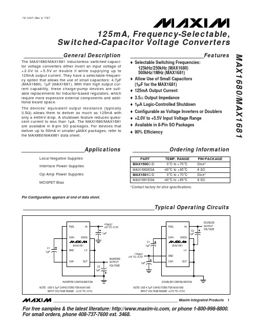
PART MAX1680C/D MAX1680ESA MAX1681C/D MAX1681ESA
TEMP. RANGE 0°C to +70°C -40°C to +85°C 0°C to +70°C -40°C to +85°C
*Contact factory for dice specifications.
Note 1: Shorting OUT to IN may damage the device and should be avoided.
Stresses beyond those listed under “Absolute Maximum Ratings” may cause permanent damage to the device. These are stress ratings only, and functional operation of the device at these or any other conditions beyond those indicated in the operational sections of the specifications is not implied. Exposure to absolute maximum rating conditions for extended periods may affect device reliability.
2.0
MAX1681
3.0
MAX1680
2.5
MAX1681
4.0
5.5 5.5
V 5.5
V 5.5
Supply Current
MAX1680 I+
MAXIM6025资料

MAX6100EURRev. ARELIABILITY REPORTFORMAX6100EURPLASTIC ENCAPSULATED DEVICESFebruary 14, 2003MAXIM INTEGRATED PRODUCTS120 SAN GABRIEL DR.SUNNYVALE, CA 94086Written byReviewed byJim Pedicord Bryan J. Preeshl Quality Assurance Quality Assurance Reliability Lab Manager Executive DirectorConclusionThe MAX6100 successfully meets the quality and reliability standards required of all Maxim products. In addition, Maxim’s continuous reliability monitoring program ensures that all outgoing product will continue to meet Maxim’s quality and reliability standards.Table of ContentsI. ........Device Description V. ........Quality Assurance InformationII. ........Manufacturing Information VI. .......Reliability EvaluationIII. .......Packaging Information IV. .......Die Information.....AttachmentsI. Device DescriptionA. GeneralThe MAX6100 is a low-cost, low-dropout (LDO), micropower voltage references. This three-terminal reference has an output voltage option of 1.8V. It features a proprietary curvature-correction circuit and laser-trimmed, thin-filmresistors that result in a low temperature coefficient of 75ppm/°C (max) and an initial accuracy of ±0.4% (max). This device is specified over the extended temperature range (-40°C to +85°C).This series-mode voltage reference draws only 90µA of supply current and can source 5mA and sink 2mA of load current. Unlike conventional shunt-mode (two-terminal) references that waste supply current and require an external resistor, this device offers a supply current that is virtually independent of the supply voltage (with only a 4µA/Vvariation with supply voltage) and does not require an external resistor. Additionally, this internally compensated device does not require an external compensation capacitor and is stable with load capacitance. Eliminating the external compensation capacitor saves valuable board area in space-critical applications. Low dropout voltage and supply-independent, ultra-low supply current makes this device ideal for battery-operated, high-performance, low-voltage systems.The MAX6100 is available in a tiny 3-pin SOT23 packages.B. Absolute Maximum RatingsItem Rating(Voltages Referenced to GND)IN -0.3V to +13.5VOUT -0.3V to (VIN + 0.3V)Output Short-Circuit to GND or IN (VIN < 6V) ContinuousOutput Short-Circuit to GND or IN (VIN = 6V) 60sOperating Temperature Range -40°C to +85°CStorage Temperature Range -65°C to +150°CLead Temperature (soldering, 10s) +300°CContinuous Power Dissipation (TA = +70°C)3-Pin SOT23 320mWDerates above +70°C3-Pin SOT23 4.0mW/°CII. Manufacturing InformationA. Description/Function: Low-Cost, Micropower, Low-Dropout, High-Output-Current, SOT23 Voltage ReferencesB. Process: B12 (Standard 1.2 micron silicon gate CMOS)C. Number of Device Transistors: 117D. Fabrication Location: California or Oregon, USAE. Assembly Location: Malaysia or ThailandF. Date of Initial Production: March, 2001III. Packaging InformationA. Package Type: 3-Pin SOT23B. Lead Frame: Copper or Alloy 42C. Lead Finish: Solder PlateD. Die Attach: Silver-filled EpoxyE. Bondwire: Gold (1.0 mil dia.)F. Mold Material: Epoxy with silica fillerG. Assembly Diagram: # 05-0901-0179H. Flammability Rating: Class UL94-V0I. Classification of Moisture Sensitivityper JEDEC standard JESD22-112: Level 1IV. Die InformationA. Dimensions: 44 x 31milsB. Passivation: Si3N4/SiO2 (Silicon nitride/ Silicon dioxide)C. Interconnect: Aluminum/Si (Si = 1%)D. Backside Metallization: NoneE. Minimum Metal Width: 1.2 microns (as drawn)F. Minimum Metal Spacing: 1.2 microns (as drawn)G. Bondpad Dimensions: 5 mil. Sq.H. Isolation Dielectric: SiO2I. Die Separation Method: Wafer SawV. Quality Assurance InformationA. Quality Assurance Contacts: Jim Pedicord (Manager, Reliability Operations)Bryan Preeshl (Executive Director)Kenneth Huening (Vice President)B. Outgoing Inspection Level: 0.1% for all electrical parameters guaranteed by the Datasheet.0.1% For all Visual Defects.C. Observed Outgoing Defect Rate: < 50 ppmD. Sampling Plan: Mil-Std-105DVI. Reliability EvaluationA. Accelerated Life TestThe results of the 135°C biased (static) life test are shown in Table 1. Using these results, the Failure Rate (λ) is calculated as follows:λ = 1 = 1.83 (Chi square value for MTTF upper limit)MTTFλ = 6.79 x 10⁻⁹λ = 6.79 F.I.T. (60% confidence level @ 25°C)This low failure rate represents data collected from Maxim’s reliability monitor program. In addition to routine production Burn-In, Maxim pulls a sample from every fabrication process three times per week and subjects it to an extended Burn-In prior to shipment to ensure its reliability. The reliability control level for each lot to be shipped as standard product is 59 F.I.T. at a 60% confidence level, which equates to 3 failures in an 80 piece sample. Maxim performs failure analysis on any lot that exceeds this reliability control level. Attached Burn-In Schematic (Spec. # 06-5630) shows the static Burn-In circuit. Maxim also performs quarterly 1000 hour life test monitors. This data is published in the Product Reliability Report (RR-1M).B. Moisture Resistance TestsMaxim pulls pressure pot samples from every assembly process three times per week. Each lot sample must meet an LTPD = 20 or less before shipment as standard product. Additionally, the industry standard 85°C/85%RH testing is done per generic device/package family once a quarter.C. E.S.D. and Latch-Up TestingThe RF24-7die type has been found to have all pins able to withstand a transient pulse of ±1500V, per Mil-Std-883 Method 3015 (reference attached ESD Test Circuit). Latch-Up testing has shown that this device withstands a current of ±250mA.Table 1Reliability Evaluation Test ResultsMAX6100EURTEST ITEM TEST CONDITION FAILURE SAMPLE NUMBER OFIDENTIFICATION PACKAGE SIZE FAILURES Static Life Test (Note 1)Ta = 135°C DC Parameters 160 0Biased & functionalityTime = 192 hrs.Moisture Testing (Note 2)Pressure Pot Ta = 121°C DC Parameters SOT 77 0P = 15 psi. & functionalityRH= 100%Time = 168hrs.85/85 Ta = 85°C DC Parameters 77 0RH = 85% & functionalityBiasedTime = 1000hrs.Mechanical Stress (Note 2)Temperature -65°C/150°C DC Parameters 77 0Cycle 1000 Cycles & functionalityMethod 1010Note 1: Life Test Data may represent plastic DIP qualification lots.Note 2: Generic Package/Process dataAttachment #1TABLE II. Pin combination to be tested. 1/ 2/1/ Table II is restated in narrative form in 3.4 below. 2/ No connects are not to be tested. 3/ Repeat pin combination I for each named Power supply and for ground (e.g., where V PS1 is V DD , V CC , V SS , V BB , GND, +V S, -V S , V REF , etc). 3.4 Pin combinations to be tested. a.Each pin individually connected to terminal A with respect to the device ground pin(s) connected to terminal B. All pins except the one being tested and the ground pin(s) shall be open. b. Each pin individually connected to terminal A with respect to each different set of a combination of all named power supply pins (e.g., V SS1, or V SS2 or V SS3 or V CC1, or V CC2) connected to terminal B. All pins except the one being tested and the power supply pin or set of pins shall be open.c.Each input and each output individually connected to terminal A with respect to a combination of all the other input and output pins connected to terminal B. All pins except the input or output pin being tested and the combination of all the other input and output pins shall be open.Terminal A (Each pin individually connected to terminal A with the other floating) Terminal B (The common combination of all like-named pins connected to terminal B) 1. All pins except V PS1 3/ All V PS1 pins 2. All input and output pinsAll other input-output pinsMil Std 883DMethod 3015.7Notice 8TERMINAL BTERMINAL APROBE(NOTE 6) R = 1.5k Ω C = 100pf。
MAX128AEAI中文资料

Typical Operating Circuit
+5V
0.1µF µC VDD SCL SDA
Applications
Industrial Control Systems Data-Acquisition Systems Robotics Automatic Testing Battery-Powered Instruments Medical Instruments
元器件交易网
19-4773; Rev 0; 7/98
KIT ATION EVALU E L B AVAILA
Multirange, +5V, 12-Bit DAS with 2-Wire Serial Interface
General Description Features
o 12-Bit Resolution, 1/2 LSB Linearity o +5V Single-Supply Operation o I2C-Compatible, 2-Wire Serial Interface o Four Software-Selectable Input Ranges MAX127: 0 to +10V, 0 to +5V, ±10V, ±5V MAX128: 0 to +VREF, 0 to +VREF/2, ±VREF, ±VREF/2 o 8 Analog Input Channels o 8ksps Sampling Rate o ±16.5V Overvoltage-Tolerant Input Multiplexer o Internal 4.096V or External Reference o Two Power-Down Modes o 24-Pin Narrow DIP or 28-Pin SSOP Packages
- 1、下载文档前请自行甄别文档内容的完整性,平台不提供额外的编辑、内容补充、找答案等附加服务。
- 2、"仅部分预览"的文档,不可在线预览部分如存在完整性等问题,可反馈申请退款(可完整预览的文档不适用该条件!)。
- 3、如文档侵犯您的权益,请联系客服反馈,我们会尽快为您处理(人工客服工作时间:9:00-18:30)。
元器件交易网
SOT23, Low-Cost, Low-Dropout, 3-Terminal Voltage References MAX6125/MAX6141/MAX6145/MAX6150/MAX6160
ABSOLUTE MAXIMUM RATINGS
(Voltages With Respect to GND) IN .......................................................................-0.3V to +13.5V OUT, ADJ...................................................-0.3V to (VIN + 0.3V) Output Short-Circuit Duration (to IN or GND).............Continuous Continuous Power Dissipation (TA = +70°C) 8-Pin SO (derate 5.9mW/°C above +70°C)....................471mW 3-Pin SOT23 (derate 4mW/°C above +70°C).................320mW 4-Pin SOT143 (derate 4mW/°C above +70°C)...............320mW Operating Temperature Range ...........................-40°C to +85°C Storage Temperature Range .............................-65°C to +160°C Lead Temperature (soldering, 10s) .................................+300°C
MAX6125/MAX6141/MAX6145/MAX6150/MAX6160
Applications
3V/5V Systems Battery-Powered Systems Portable and Hand-Held Equipment Data-Acquisition Systems Instrumentation and Process Control
IN 1
GND 1
4
OUT
MAX6125 MAX6141 MAX6145 MAX6150 MAX6160
7 6 5
OUT 2
MAX6125 MAX6141 MAX6145 MAX6150 SOT23-3
MAX6160 3 GND
ADJ 2 3 IN
SO
( ) ARE FOR MAX6160 ONLY
Features
♦ 3-Pin SOT23 Package (MAX6125/MAX6141/MAX6145/MAX6150) 4-Pin SOT143 Package (MAX6160) ♦ Low, 200mV Dropout Voltage ♦ 75µA Supply Current, Independent of Input Voltage ♦ 15ppm/°C Typical Tempco (50ppm/°C, max) ♦ Stable for All Capacitive Loads up to 10nF ♦ Adjustable Output Voltage from 1.23V to (VIN - 0.2V) (MAX6160) ♦ Optimized for 3V/5V Operation
∆VOUT/∆VIN VIN = 2.7V to 12.6V, TA = TMIN to TMAX ∆VOUT/∆IOUT IQ ∆IQ/CTERISTICS—MAX6141
(VIN = 4.3V, IOUT = 0mA, TA = +25°C, unless otherwise noted.) (Note 1) PARAMETER Supply Voltage Output Voltage Output Voltage Temperature Coefficient Output Voltage Noise Line Regulation Load Regulation Quiescent Supply Current Change in Supply Current vs. Change in Input Voltage 2 SYMBOL VIN VOUT TCVOUT en TA = +25°C TA = TMIN to TMAX TA = TMIN to TMAX 0.1Hz to 10Hz 10Hz to 10kHz ISOURCE = 0mA to 1mA ISINK = 0mA to 1mA TA = +25°C TA = TMIN to TMAX VIN = 4.3V to 12.6V 1.7 CONDITIONS TA = TMIN to TMAX MIN 4.3 4.055 4.015 15 25 700 2 0.55 1.65 78 50 1.6 16 105 130 6 4.096 TYP MAX 12.6 4.140 4.180 50 UNITS V V ppm/°C µVP-P µV/V mV/mA µA µA/V
SOT143-4
________________________________________________________________ Maxim Integrated Products
1
For pricing, delivery, and ordering information, please contact Maxim/Dallas Direct! at 1-888-629-4642, or visit Maxim’s website at .
元器件交易网
19-1177; Rev. 1; 10/02
SOT23, Low-Cost, Low-Dropout, 3-Terminal Voltage References
General Description
The MAX6125/MAX6141/MAX6145/MAX6150/MAX6160 low-dropout, micropower, three-terminal voltage references offer 2.5V, 4.096V, 4.5V, 5.0V, and adjustable (1.23V to 12.4V) output voltages, respectively. Low, 200mV dropout makes these devices ideal for 3V and 5V systems. Unlike two-terminal references that waste battery current and require an external resistor, the MAX61xx family’s supply current is virtually independent of input voltage variations, which translates to longer battery life. Initial accuracy for these devices is ±1%. The output temperature coefficient is typically 15ppm/°C, and guaranteed to be less than 50ppm/°C (except for the MAX6160). The MAX6125/MAX6141/MAX6145/ MAX6150 are available in 3-pin SOT23 and 8-pin SO packages. The MAX6160 is available in 4-pin SOT143 and 8-pin SO packages.
Stresses beyond those listed under “Absolute Maximum Ratings” may cause permanent damage to the device. These are stress ratings only, and functional operation of the device at these or any other conditions beyond those indicated in the operational sections of the specifications is not implied. Exposure to absolute maximum rating conditions for extended periods may affect device reliability.
ELECTRICAL CHARACTERISTICS—MAX6125
(VIN = 2.7V, IOUT = 0mA, TA = +25°C, unless otherwise noted.) (Note 1) PARAMETER Supply Voltage Output Voltage Output Voltage Temperature Coefficient Output Voltage Noise Line Regulation Load Regulation Quiescent Supply Current Change in Supply Current vs. Change in Input Voltage SYMBOL VIN VOUT TCVOUT en TA = +25°C TA = TMIN to TMAX TA = TMIN to TMAX 0.1Hz to 10Hz 10Hz to 10kHz ISOURCE = 0mA to 1mA ISINK = 0mA to 1mA TA = +25°C TA = TMIN to TMAX VIN = 2.7V to 12.6V 1.7 CONDITIONS TA = TMIN to TMAX MIN 2.7 2.475 2.450 15 15 500 1 0.4 1.15 75 50 1 10 100 130 6 2.500 TYP MAX 12.6 2.525 2.550 50 UNITS V V ppm/°C µVP-P µV/V mV/mA µA µA/V