FCN2416E563K-D4中文资料
24lc256系列中文
1.8-5.5V 400 kHz (2) 2.5-5.5V 400 kHz 1.8-5.5V 400 kHz(2) 2.5-5.5V 400 kHz 4.5V-5.5V 400 kHz
8 字节
16 字节 16 字节
整个阵列
整个阵列 无
无
A0, A1, A2 A0, A1, A2
I I, E
I I C, I, E
装。
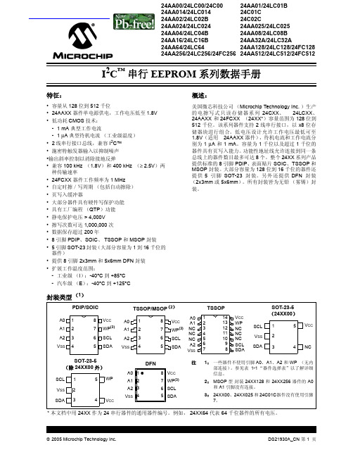
封装类型 (1)
PDIP/SOIC
TSSOP/MSOP(2)
A0 1 A1 2 A2 3 VSS 4
8 VCC
A0 1
7 WP(3) A1 2
6 SCL
A2 3
5 SDA VSS 4
8 VCC
A0 A1
7 WP(3) NC NC
6 SCL NC
5
SDA
A2 VSS
TSSOP
1
14
2
13
3
12
4
11
1.8-5.5V 2.5-5.5V 1.8-5.5V
400 kHz (2)
400 kHz 1 MHz(3)
64 字节
整个阵列
A0, A1, A2(4)
I
P, SN, SM, ST, MS, MF,
I, E ST14
I
256 千位器件
24AA256
1.8-5.5V 400 kHz (2)
24LC256 24FC256
2005 Microchip Technology Inc.
DS21930A_CN 第 3 页
24AAXX/24LCXX/24FCXX
2.0 电气特性
绝对最大额定值 (†)
VCC.............................................................................................................................................................................6.5V 相对于 Vss 的所有输入和输出 ............................................................................................................ -0.6V 到 VCC +1.0V 存储温度 ................................................................................................................................................. -65°C 到 +150°C 环境温度 (使用电源时)........................................................................................................................ -40°C 到 +125°C 所有引脚静电保护 ....................................................................................................................................................................≥ 4 kV
FCN1913E223K-E2中文资料

SpecificationsType FCN capacitors are designed for applicationsrequiring a general purpose SMT capacitor with stabletemperature and frequency characteristics similar topolyester film capacitors. They are ideal for applicationssuch as EMI noise filtering, power supply input/outputfilters, audio or signal coupling, and IC power busbypassing or decoupling. FCN SMT capacitors have anon-inductive stacked metallized PEN film constructionwhich results in a low ESR and excellent high frequencyperformance.HighlightsDesigned for reflow solderingWithstands 150% of rated voltage for 60 secondsStacked metallized polyethylene naphthalate(PEN) filmPerforms like polyester capacitorsNonmagnetic and lead-free•••••Capacitance Range:Capacitance Tolerance:Voltages:Operating Temperature Range:IR (at 20 ºC, after 60 seconds):Dissipation Factor (Tanδ):Life Test:Moisture Resistance:1000 pF to 1.0 µF (1 kHz at 5 Vrms)±5% (J), ±10% (K) (See Ratings)16, 50, 100, 250 & 400 Vdc16, 50, 100Vdc (<0.012 µF);–55 ºC to +105 ºC100 Vdc (≥ 0.012 µF), 250, 400 Vdc;–40 ºC to +85 ºCC >0.33 µF: IR = 1000 MΩ•µF Min.C ≤0.33 µF: IR ≥ 3000 MΩ1.0% Max. (1 kHz at 5 Vrms)1000 h at rated temp. & 125% rated voltage∆ Capacitance: +1%, –6% maxDissipation Factor: 1.1% maxIR: 1000 MΩmin (C>0.33 µF, 300 MΩ•µF min)No significant visual damage1000 h at 40 ºC and 90 - 95% RH & rated voltage∆ Capacitance: +8/-5%Dissipation Factor: 1.5% maxIR: 100 MΩ min (C >0.33 µF, 30 MΩ•µF min)Voltage withstanding: 1.3 times rated voltage,1 min.No significant damageStable Stacked Metallized Film (PEN) Chips for Reflow SolderingT ype FCN SMT capacitors are the general purpose line of CDE’ssurface mount product offerings. They range in capacitance from.001 µF to 1.0 µF, and they are available in voltage ratings up to400 Vdc.Complies with the EU Directive2002/95/E C r e q u i r e m e n trestricting the use of Lead (Pb),Mercury (Hg), Cadmium (Cd),Hexavalent chromium (Cr(VI)),PolyBrominated Biphenyls (PBB)and PolyBrominated DiphenylEthers (PBDE).Part Numbering SystemSpecificationsResistance to Soldering Heat:5 s at max capacitor surface temperature ∆ Capacitance: ±5% maxDissipation Factor: 1.1% maxIR: 1000 MΩ min (C >0.33 µF, 300 MΩ•µF min)Voltage withstanding: 1.5 times rated voltage, 1 min.No significant visual damage.Surface Temperature:16 V & 50 V & 100 V ≤ 0.01 µF: 240 ºC max 100 V ≥ 0.012 µF, 250 V & 400 V: 230 ºC maxMoisture Resistance:500 h at 85 ºC and 85% RH ∆ Capacitance: ±10% max Dissipation Factor: 2% maxIR: 10 MΩ min (C >0.33 µF, 3 MΩ•µF min) Voltage withstanding: 1.3 times rated voltage, 1 min.No significant damageWithstand Voltage:16 V & 50 V, 100 V ≤ 0.01 µF: 175% rated voltage, 5 s100 V ≥ 0.012 µF, 250 V and 400 V: 150% rated voltage, 5 sFCN1206A102JH2TapeTape PackagingWidth Diameter Reel Type Case SizeVoltage Capacitance Tolerance Code (mm)[in.(mm)]QuantityFCN1206C = 16 Vdc 102 = 0.001 µF J = ±5%K1=87 (178)40001913H = 50 Vdc 223 = 0.022 µF K = ±10%J1, J2=87 (178)30002416 A = 100 Vdc 474 = 0.47 µFH1, H2=87 (178)30002420E = 250 Vdc H3=87 (178)20002820G = 400 VdcG1, G2, G3=87 (178)20003022E1, E2=1213 (330)30003925E3, E4=1213 (330)20003931D1, D2=1213 (330)30006031D3, D4, D5=1213 (330)20006040B, Z =1213 (330)1500U, V, X, Y =1613 (330)1000S, T=2413 (330)750Outline Drawingt L WTt = 0.014 ± 0.008 in. (0.35 ±0.2 mm)For 0.001 µF – 0.01 µF, 100 V, t = 0.026 ±0.012 in. (0.62 ± 0.3 mm) RatingsCap Catalog L W T(µF)Part Number in (mm)in (mm)in (mm)16 Vdc.12FCN1913C124J-E10.189±0.008 (4.8±0.2)0.130±0.012 (3.3±0.3)0.055±0.008 (1.4±0.2) .15FCN1913C154J-E20.189±0.008 (4.8±0.2)0.130±0.012 (3.3±0.3)0.079±0.008 (2.0±0.2) .18FCN1913C184J-E20.189±0.008 (4.8±0.2)0.130±0.012 (3.3±0.3)0.079±0.008 (2.0±0.2) .22FCN1913C224J-E40.189±0.008 (4.8±0.2)0.130±0.012 (3.3±0.3)0.094±0.008 (2.4±0.2) .27FCN2416C274J-D10.236±0.008 (6.0±0.2)0.161±0.012 (4.1±0.3)0.071±0.008 (1.8±0.2) .33FCN2416C334J-D20.236±0.008 (6.0±0.2)0.161±0.012 (4.1±0.3)0.079±0.008 (2.0±0.2) .39FCN2416C394J-D30.236±0.008 (6.0±0.2)0.161±0.012 (4.1±0.3)0.094±0.008 (2.4±0.2) .47FCN2416C474J-D40.236±0.008 (6.0±0.2)0.161±0.012 (4.1±0.3)0.110±0.008 (2.8±0.2)50 Vdc.056FCN1913H563J-E20.189±0.008 (4.8±0.3)0.130±0.012 (3.3±0.3)0.055±0.008 (1.4±0.2) .068FCN1913H683J-E20.189±0.008 (4.8±0.3)0.130±0.012 (3.3±0.3)0.079±0.008 (2.0±0.2) .082FCN1913H823J-E40.189±0.008 (4.8±0.3)0.130±0.012 (3.3±0.3)0.079±0.008 (2.0±0.2) .10FCN1913H104J-E30.189±0.008 (4.8±0.3)0.130±0.012 (3.3±0.3)0.094±0.008 (2.4±0.2) .12FCN2416H124J-D10.236±0.008 (6.0±0.2)0.161±0.012 (4.1±0.3)0.071±0.008 (1.8±0.2) .15FCN2416H154J-D20.236±0.008 (6.0±0.2)0.161±0.012 (4.1±0.3)0.079±0.008 (2.0±0.2) .18FCN2416H184J-D30.236±0.008 (6.0±0.2)0.161±0.012 (4.1±0.3)0.094±0.008 (2.4±0.2) .22FCN2416H224J-D40.236±0.008 (6.0±0.2)0.161±0.012 (4.1±0.3)0.110±0.008 (2.8±0.2)100 Vdc.0010FCN1206A102J-H20.126±0.008 (3.2±0.2)0.063±0.012 (1.6±0.3)0.043±0.008 (1.1±0.2) .0012FCN1206A122J-H20.126±0.008 (3.2±0.2)0.063±0.012 (1.6±0.3)0.043±0.008 (1.1±0.2) .0015FCN1206A152J-H20.126±0.008 (3.2±0.2)0.063±0.012 (1.6±0.3)0.043±0.008 (1.1±0.2) .0018FCN1206A182J-H20.126±0.008 (3.2±0.2)0.063±0.012 (1.6±0.3)0.043±0.008 (1.1±0.2) .0022FCN1206A222J-H20.126±0.008 (3.2±0.2)0.063±0.012 (1.6±0.3)0.043±0.008 (1.1±0.2) .0027FCN1206A272J-H20.126±0.008 (3.2±0.2)0.063±0.012 (1.6±0.3)0.043±0.008 (1.1±0.2) .0033FCN1206A332J-H30.126±0.008 (3.2±0.2)0.063±0.012 (1.6±0.3)0.059±0.008 (1.5±0.2) .0039FCN1206A392J-H30.126±0.008 (3.2±0.2)0.063±0.012 (1.6±0.3)0.059±0.008 (1.5±0.2) .0047FCN1206A472J-H30.126±0.008 (3.2±0.2)0.063±0.012 (1.6±0.3)0.059±0.008 (1.5±0.2) .0056FCN1210A562J-G20.126±0.008 (3.2±0.2)0.063±0.012 (1.6±0.3)0.059±0.008 (1.5±0.2) .0068FCN1210A682J-G20.126±0.008 (3.2±0.2)0.063±0.012 (1.6±0.3)0.059±0.008 (1.5±0.2) .0082FCN1210A822J-G30.126±0.008 (3.2±0.2)0.063±0.012 (1.6±0.3)0.083±0.008 (2.1±0.2) .010FCN1210A103J-G30.126±0.008 (3.2±0.2)0.063±0.012 (1.6±0.3)0.083±0.008 (2.1±0.2) .012FCN1913A123K-E10.189±0.008 (4.8±0.2)0.189±0.008 (3.3±0.3)0.055±0.008 (1.4±0.2) .015FCN1913A153K-E10.189±0.008 (4.8±0.2)0.189±0.008 (3.3±0.3)0.055±0.008 (1.4±0.2) .018FCN1913A183K-E10.189±0.008 (4.8±0.2)0.189±0.008 (3.3±0.3)0.055±0.008 (1.4±0.2) .022FCN1913A223K-E10.189±0.008 (4.8±0.2)0.189±0.008 (3.3±0.3)0.055±0.008 (1.4±0.2) .027FCN1913A273K-E10.189±0.008 (4.8±0.2)0.189±0.008 (3.3±0.3)0.055±0.008 (1.4±0.2) .033FCN1913A333K-E10.189±0.008 (4.8±0.2)0.189±0.008 (3.3±0.3)0.055±0.008 (1.4±0.2) .039FCN1913A393K-E10.189±0.008 (4.8±0.2)0.189±0.008 (3.3±0.3)0.055±0.008 (1.4±0.2)Cap Catalog L W T(µF)Part Number in (mm)in (mm)in (mm)100 Vdc.047FCN1913A473K-E20.189±0.008 (4.8±0.2)0.189±0.008 (3.3±0.3)0.079±0.008 (2.0±0.2) .056FCN1913A563K-E20.189±0.008 (4.8±0.2)0.189±0.008 (3.3±0.3)0.079±0.008 (2.0±0.2) .068FCN1913A683K-E40.189±0.008 (4.8±0.2)0.189±0.008 (3.3±0.3)0.094±0.008 (2.4±0.2) .082FCN1913A823K-E30.189±0.008 (4.8±0.2)0.189±0.008 (3.3±0.3)0.110±0.012 (2.8±0.3) .10FCN2416A104K-D10.189±0.008 (4.8±0.2)0.236±0.008 (6.0±0.2)0.071±0.012 (1.8±0.3) .12FCN2416A124K-D3*0.189±0.008 (4.8±0.2)0.236±0.008 (6.0±0.2)0.099±0.012 (2.4±0.3) .15FCN2416A154K-D4*0.189±0.008 (4.8±0.2)0.236±0.008 (6.0±0.2)0.110±0.012 (2.8±0.3) .18FCN2820A184K-Z0.280±0.016 (7.1±0.4)0.197±0.016 (5.0±0.4)0.079±0.012 (2.0±0.3) .22FCN2820A224K-Z0.280±0.016 (7.1±0.4)0.197±0.016 (5.0±0.4)0.094±0.012 (2.4±0.3) .27FCN2820A274K-Z0.280±0.016 (7.1±0.4)0.197±0.016 (5.0±0.4)0.114±0.012 (2.9±0.3) .33FCN2820A334K-Z0.280±0.016 (7.1±0.4)0.197±0.016 (5.0±0.4)0.138±0.012 (3.5±0.3) .39FCN3022A394K-X0.303±0.016 (7.7±0.4)0.217±0.016 (5.5±0.4)0.134±0.012 (3.4±0.3) .47FCN3022A474K-X0.303±0.016 (7.7±0.4)0.217±0.016 (5.5±0.4)0.157±0.012 (4.0±0.3) .56FCN3925A564K-V0.386±0.016 (9.8±0.4)0.248±0.016 (6.3±0.4)0.118±0.012 (3.0±0.3) .68FCN3925A684K-V0.386±0.016 (9.8±0.4)0.248±0.016 (6.3±0.4)0.142±0.012 (3.6±0.3) .82FCN3925A824K-V0.386±0.016 (9.8±0.4)0.248±0.016 (6.3±0.4)0.169±0.012 (4.3±0.3) 1.0FCN3925A105K-V0.386±0.016 (9.8±0.4)0.248±0.016 (6.3±0.4)0.201±0.012 (5.1±0.3)250 Vdc.0010FCN1913E102K-E1*0.189±0.008 (4.8±0.2)0.130±0.012 (3.3±0.3)0.055±0.008 (1.4±0.2) .0012FCN1913E122K-E1*0.189±0.008 (4.8±0.2)0.130±0.012 (3.3±0.3)0.055±0.008 (1.4±0.2) .0015FCN1913E152K-E1*0.189±0.008 (4.8±0.2)0.130±0.012 (3.3±0.3)0.055±0.008 (1.4±0.2) .0018FCN1913E182K-E1*0.189±0.008 (4.8±0.2)0.130±0.012 (3.3±0.3)0.055±0.008 (1.4±0.2) .0022FCN1913E222K-E1*0.189±0.008 (4.8±0.2)0.130±0.012 (3.3±0.3)0.055±0.008 (1.4±0.2) .0027FCN1913E272K-E1*0.189±0.008 (4.8±0.2)0.130±0.012 (3.3±0.3)0.055±0.008 (1.4±0.2) .0033FCN1913E332K-E1*0.189±0.008 (4.8±0.2)0.130±0.012 (3.3±0.3)0.055±0.008 (1.4±0.2) .0039FCN1913E392K-E1*0.189±0.008 (4.8±0.2)0.130±0.012 (3.3±0.3)0.055±0.008 (1.4±0.2) .0047FCN1913E472K-E1*0.189±0.008 (4.8±0.2)0.130±0.012 (3.3±0.3)0.055±0.008 (1.4±0.2) .0056FCN1913E562K-E1*0.189±0.008 (4.8±0.2)0.130±0.012 (3.3±0.3)0.055±0.008 (1.4±0.2) .0068FCN1913E682K-E1*0.189±0.008 (4.8±0.2)0.130±0.012 (3.3±0.3)0.055±0.008 (1.4±0.2) .0082FCN1913E822K-E1*0.189±0.008 (4.8±0.2)0.130±0.012 (3.3±0.3)0.055±0.008 (1.4±0.2) .010FCN1913E103K-E1*0.189±0.008 (4.8±0.2)0.130±0.012 (3.3±0.3)0.055±0.008 (1.4±0.2) .012FCN1913E123K-E1*0.189±0.008 (4.8±0.2)0.130±0.012 (3.3±0.3)0.055±0.008 (1.4±0.2) .015FCN1913E153K-E1*0.189±0.008 (4.8±0.2)0.130±0.012 (3.3±0.3)0.055±0.008 (1.4±0.2) .018FCN1913E183K-E2*0.189±0.008 (4.8±0.2)0.130±0.012 (3.3±0.3)0.079±0.008 (2.0±0.2) .022FCN1913E223K-E2*0.189±0.008 (4.8±0.2)0.130±0.012 (3.3±0.3)0.094±0.008 (2.4±0.2) .027FCN1913E273K-E4*0.189±0.008 (4.8±0.2)0.130±0.012 (3.3±0.3)0.110±0.008 (2.8±0.2) .033FCN1913E333K-E3*0.189±0.008 (4.8±0.2)0.130±0.012 (3.3±0.3)0.126±0.008 (3.2±0.2) .039FCN2416E393K-D2*0.236±0.008 (6.0±0.2)0.161±0.012 (4.1±0.3)0.079±0.008 (2.0±0.2) .047FCN2416E473K-D3*0.236±0.008 (6.0±0.2)0.161±0.012 (4.1±0.3)0.079±0.008 (2.0±0.2) .056FCN2416E563K-D4*0.236±0.008 (6.0±0.2)0.161±0.012 (4.1±0.3)0.094±0.008 (2.4±0.2) .068FCN2416E683K-D5*0.236±0.008 (6.0±0.2)0.161±0.012 (4.1±0.3)0.110±0.008 (2.8±0.2) .082FCN2420E823K-B*0.236±0.008 (6.0±0.2)0.197±0.016 (5.0±0.4)0.126±0.012 (3.2±0.3) .10FCN2420E104K-B*0.236±0.008 (6.0±0.2)0.197±0.016 (5.0±0.4)0.150±0.012 (3.8±0.3) .12FCN2420E124K-B*0.236±0.008 (6.0±0.2)0.197±0.016 (5.0±0.4)0.177±0.012 (4.5±0.3) .15FCN2825E154K-Y 0.280±0.016 (7.1±0.4)0.248±0.016 (6.3±0.4)0.138±0.012 (3.5±0.3) .18FCN2825E184K-Y 0.280±0.016 (7.1±0.4)0.248±0.016 (6.3±0.4)0.161±0.012 (4.1±0.3) .22FCN2825E224K-Y 0.280±0.016 (7.1±0.4)0.248±0.016 (6.3±0.4)0.201±0.012 (5.1±0.3) .27FCN3925E274K-V 0.386±0.020 (9.8±0.5)0.248±0.016 (6.3±0.4)0.154±0.012 (3.9±0.3)Cap Catalog L W T(µF)Part Number in (mm)in (mm)in (mm)250 Vdc.33FCN3925E334K-V 0.386±0.020 (9.8±0.5)0.248±0.016 (6.3±0.4)0.189±0.012 (4.8±0.3) .39FCN3931E394K-U 0.386±0.020 (9.8±0.5)0.315±0.016 (8.0±0.4)0.173±0.012 (4.4±0.3) .47FCN3931E474K-U 0.386±0.020 (9.8±0.5)0.315±0.016 (8.0±0.4)0.209±0.012 (5.3±0.3) .56FCN6031E564K-T 0.598±0.020 (15.2±0.5)0.315±0.016 (8.0±0.4)0.146±0.012 (3.7±0.3) .68FCN6031E684K-T 0.598±0.020 (15.2±0.5)0.315±0.016 (8.0±0.4)0.173±0.012 (4.4±0.3) .82FCN6040E824K-S 0.598±0.020 (15.2±0.5)0.394±0.016 (10.0±0.4)0.165±0.012 (4.2±0.3) 1.0FCN6040E105K-S 0.598±0.020 (15.2±0.5)0.394±0.016 (10.0±0.4)0.201±0.012 (5.1±0.3)400 Vdc.0010FCN1913G102J-E10.189±0.008 (4.8±0.2) 0.130±0.012 (3.3±0.3) 0.055±0.008 (1.4±0.2) .0012FCN1913G122J-E1 0.189±0.008 (4.8±0.2) 0.130±0.012 (3.3±0.3) 0.055±0.008 (1.4±0.2) .0015FCN1913G152J-E1 0.189±0.008 (4.8±0.2) 0.130±0.012 (3.3±0.3) 0.055±0.008 (1.4±0.2) .0018FCN1913G182J-E1 0.189±0.008 (4.8±0.2) 0.130±0.012 (3.3±0.3) 0.055±0.008 (1.4±0.2) .0022FCN1913G222J-E1 0.189±0.008 (4.8±0.2) 0.130±0.012 (3.3±0.3) 0.055±0.008 (1.4±0.2) .0027FCN1913G272J-E1 0.189±0.008 (4.8±0.2) 0.130±0.012 (3.3±0.3) 0.055±0.008 (1.4±0.2) .0033FCN1913G332J-E1 0.189±0.008 (4.8±0.2) 0.130±0.012 (3.3±0.3) 0.055±0.008 (1.4±0.2) .0039FCN1913G392J-E1 0.189±0.008 (4.8±0.2) 0.130±0.012 (3.3±0.3) 0.055±0.008 (1.4±0.2) .0047FCN1913G472J-E1 0.189±0.008 (4.8±0.2) 0.130±0.012 (3.3±0.3) 0.055±0.008 (1.4±0.2) .0056FCN1913G562J-E2 0.189±0.008 (4.8±0.2) 0.130±0.012 (3.3±0.3) 0.079±0.008 (2.0±0.2) .0068FCN1913G682J-E2 0.189±0.008 (4.8±0.2) 0.130±0.012 (3.3±0.3) 0.079±0.008 (2.0±0.2) .0082FCN1913G822J-E4 0.189±0.008 (4.8±0.2) 0.130±0.012 (3.3±0.3) 0.094±0.008 (2.4±0.2) .010FCN1913G103J-E3 0.189±0.008 (4.8±0.2) 0.130±0.012 (3.3±0.3) 0.110±0.008 (2.8±0.2) .012FCN2416G123J-D2 0.236±0.008 (6.0±0.2) 0.161±0.012 (4.1±0.3) 0.079±0.008 (2.0±0.2) .015FCN2416G153J-D3 0.236±0.008 (6.0±0.2) 0.161±0.012 (4.1±0.3) 0.079±0.008 (2.0±0.2) .018FCN2416G183J-D4 0.236±0.008 (6.0±0.2) 0.161±0.012 (4.1±0.3) 0.110±0.008 (2.8±0.2) .022FCN2416G223J-D5 0.236±0.008 (6.0±0.2) 0.161±0.012 (4.1±0.3) 0.126±0.012 (3.2±0.3) .027FCN2420G273J-B 0.236±0.008 (6.0±0.2) 0.197±0.016 (5.0±0.4) 0.118±0.012 (3.0±0.3) .033FCN2420G333J-B 0.236±0.008 (6.0±0.2) 0.197±0.016 (5.0±0.4) 0.142±0.012 (3.6±0.3) .039FCN2820G393J-Z 0.280±0.016 (7.1±.0.4) 0.197±0.016 (5.0±0.4) 0.126±0.012 (3.2±0.3) .047FCN2820G473J-Z 0.280±0.016 (7.1±.0.4) 0.197±0.016 (5.0±0.4) 0.150±0.012 (3.8±0.3) .056FCN2825G563J-Y 0.280±0.016 (7.1±.0.4) 0.248±0.016 (6.3±0.4) 0.142±0.012 (3.6±0.3) .068FCN2825G683J-Y0.280±0.016 (7.1±.0.4) 0.248±0.016 (6.3±0.4) 0.173±0.012 (4.4±0.3) .082FCN3925G823J-V 0.386±0.016 (9.8±0.4)0.248±0.016 (6.3±0.4) 0.134±0.012 (3.4±0.3) .10FCN3925G104J-V 0.386±0.016 (9.8±0.4)0.248±0.016 (6.3±0.4) 0.157±0.012 (4.0±0.3) .12FCN3931G124J-U 0.386±0.016 (9.8±0.4)0.315±0.016 (8.0±0.4) 0.150±0.012 (3.8±0.3) .15FCN3931G154J-U 0.386±0.016 (9.8±0.4)0.315±0.016 (8.0±0.4) 0.181±0.012 (4.6±0.3)Typical Temperature Characteristics Typical Frequency CharacteristicsVrms vs. Frequency CharacteristicsPulse Handling CapabilityTypical ApplicationsDC Blocking for xDSLIntegration for Electroluminescent (EL) DriverWith no piezoelectric effects to deal with, the SMT film capacitor will not create electrical noise in signal circuits or bu zz ing in power circuits.CapacitanceVoltage dV/dt Capacitance VoltagedV/dt CapacitanceVoltage dV/dt (µF)(Vdc)(volts/µsec)(µF)(Vdc)(volts/µsec)(µF)(Vdc)(volts/µsec).12 - .221660.0039100530.001 - .0039250615.27 - .471640.0047100480.0047 - .033250360.056 - .1050190.0056100450.039 - .12250240.12 - .2250130.0068100410.15 - .22250190.0011001000.0082100370.27 - .47250115.0012100920.01100340.56 - 1.025065.0015100830.012 - .082100320.001 - .0039400615.0018100760.10 - .15100210.0047 - .01400360.0022100690.18 - .33100120.012 - .033400240.0027100630.39 - .47100100.039 - .068400190.0033100570.056 - 1.010070.082 - .15400115。
FR24中文资料
25 50 75 100 125 150 175 ° Ambient Temperature (°C)
100 10 Number of Cycles @ 60 Hz
Typical Instantaneous Forward Characteristics 100 Forward Current (A)
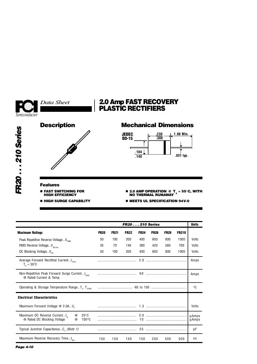
FR20 . . . 210 Series Maximum Ratings Peak Repetitive Reverse Voltage...VRRM RMS Reverse Voltage...VR(rms) DC Blocking Voltage...VDC Average Forward Rectified Current...IF(av) TA = 55°C Non-Repetitive Peak Forward Surge Current...IFSM @ Rated Current & Temp Operating & Storage Temperature Range...TJ, TSTRG Electrical Characteristics Maximum Forward Voltage @ 2.0A...VF Maximum DC Reverse Current...IR @ Rated DC Blocking Voltage @ @ 25°C 100°C ............................................. 1.3 ............................................... FR20 50 35 50 FR21 100 70 100 FR22 200 140 200 FR24 400 280 400 FR26 600 420 600 FR28 800 560 800 FR210 1000 700 1000
数字多用表

®
8845A/8846A
数字多用表
用户手册
July 2006
© 2006 Fluke Corporation. All rights reserved. All product names are trademarks of their respective companies.
目 录
章节
标题
页
概述和技术指标 ................................................................................................. 1-1 概述 ...................................................................................................................1-3 用户文件 ...........................................................................................................1-3 关于本手册 .......................................................................................................1-3 安全信息 ...........................................................................................................1-4 通用安全事项 ...............................................................................................1-4 符号和标记 ...................................................................................................1-6 仪器安全程序 ...................................................................................................1-6 易失性存储器 ...............................................................................................1-6 非易失性存储器 ...........................................................................................1-7 存储介质(仅限 8846A) ...........................................................................1-7 附件 ...................................................................................................................1-7 通用技术指标 ...................................................................................................1-9 电源 ...............................................................................................................1-9 尺寸 ...............................................................................................................1-9 显示屏 ...........................................................................................................1-9 环境 ...............................................................................................................1-9 安全 ...............................................................................................................1-9 电磁兼容(EMC) ......................................................................................1-9 触发 ...............................................................................................................1-9 存储器 ...........................................................................................................1-10 计算功能 .......................................................................................................1-10 电气 ...............................................................................................................1-10 程控接口 .......................................................................................................1-10 质量保证期 ...................................................................................................1-10 电气技术指标 ...................................................................................................1-10 直流电压技术指标 .......................................................................................1-10 交流电压技术指标 .......................................................................................1-11 电阻 ...............................................................................................................1-13 直流电流 .......................................................................................................1-15 交流电流 .......................................................................................................1-16 频率 ...............................................................................................................1-18
CAT24FC16YITE13资料

i n ue dPa rt 1© 2005 by Catalyst Semiconductor, Inc.Characteristics subject to change without notice.Doc. No. 1054, Rev. I* Catalyst Semiconductor is licensed by Philips Corporation to carry the I 2C Bus Protocol.PIN CONFIGURATIONBLOCK DIAGRAMPIN FUNCTIONSPin Name Function NC No Connect SDA Serial Data/Address SCL Serial Clock WP Write ProtectV CC2.5 V to 5.5 V Power Supply V SSGroundDIP Package (P, L)TSSOP Package (U, Y)SOIC Package (J, W)FEATURESI 400 kHz (2.5 V) I 2C bus compatible I 2.5 to 5.5 volt operation I Low power CMOS technology I 16-byte page write bufferI Industrial and extended temperature ranges I Self-timed write cycle with auto-clear I 1,000,000 program/erase cyclesI 100 year data retentionI 8-pin DIP, SOIC, TSSOP, MSOP and TDFNpackages- “Green” package option availableI 2,048 x 8 memory organization I Hardware write protectDESCRIPTIONThe CAT24FC16 is a 16-kb Serial CMOS EEPROM internally organized as 2048 words of 8 bits each.Catalyst’s advanced CMOS technology substantially reduces device power requirements. The CAT24FC16features a 16-byte page write buffer. The device operates via the I 2C bus serial interface and is available in 8-pin DIP, SOIC, TSSOP, MSOP and TDFN packages.EXTERNAL LOADTDFN Package (RD4, ZD4)SSV V V CC WP SCL SDAMSOP Package (R, Z)V CC WP SCL SDAV CC WP SCL SDANC NC NC V SSNC NC NCV SSV CC WP SCL SDANC NC NCV SSDis co n ti n ue dPa rt CAT24FC162Doc. No. 1054, Rev. ICAPACITANCE T A = 25°C, f = 400 kHz, V CC = 5 V Symbol TestConditions MinTyp Max Units C I/O (3)Input/Output Capacitance (SDA)V I/O = 0 V 8pF C IN (3)Input Capacitance (other pins)V IN = 0 V6pFRELIABILITY CHARACTERISTICS (3)Symbol Parameter MinTyp Max Un itsN END Endurance 1,000,000Cycles/Byte T DR Data Retention 100Years V ZAP ESD Susceptibility4000Volts I LTH (4)Latch-up100mAABSOLUTE MAXIMUM RATINGS*Temperature Under Bias–55°C to +125°CStorage Temperature.......................–65°C to +150°C Voltage on Any Pin withRespect to Ground (1)............–2.0 V to V CC + 2.0 V V CC with Respect to Ground .............–2.0 V to +7.0 V Package Power DissipationCapability (T A = 25°C)..................................1.0 W Note:(1)The minimum DC input voltage is –0.5 V. During transitions, inputs may undershoot to –2.0 V for periods of less than 20 ns. Maximum DCvoltage on output pins is V CC + 0.5 V, which may overshoot to V CC + 2.0 V for periods of less than 20 ns.(2)Output shorted for no more than one second. No more than one output shorted at a time.(3)These parameters are tested initially and after a design or process change that affects the parameter according to appropriate AEC-Q100and JEDEC test methods.(4)Latch-up protection is provided for stresses up to 100 mA on address and data pins from –1.0 V to V CC + 1.0 V.(5)Maximum standby current (I SB ) = 10µA for the Extended Automotive temperature range.D.C. OPERATING CHARACTERISTICSV CC = 2.5 V to 5.5 V, unless otherwise specified.Symbol ParameterTest ConditionsMin TypMax Units I CC Power Supply Current (Read)f SCL = 400 kHz 1mA I CC Power Supply Current (Write)f SCL = 400 kHz3mA I SB (5)Standby Current (V CC = 5.0 V)V IN = GND or V CC 1µA I LI Input Leakage Current V IN = GND to V CC1µA I LO Output Leakage Current V OUT = GND to V CC1µA V IL Input Low Voltage –1V CC x 0.3V V IH Input High VoltageV CC x 0.7V CC + 1.0V V OLOutput Low Voltage (V CC = 3.0 V)I OL = 3 mA 0.4VLead Soldering Temperature (10 seconds)......300°C Output Short Circuit Current (2).......................100 mA*COMMENTStresses above those listed under “Absolute Maximum Ratings ” may cause permanent damage to the device. These are stress ratings only,and functional operation of the device at these or any other conditions outside of those listed in the operational sections of this specification is not implied. Exposure to any absolute maximum rating for extended periods may affect device performance and reliability.Dis co n ti n ue dPa rt CAT24FC163Doc No. 1054, Rev. IWrite Cycle Limits Symbol ParameterMinTyp Max Un its t WRWrite Cycle Time5msA.C. CHARACTERISTICSV CC = 2.5 V to 5.5 V, unless otherwise specified.Read & Write Cycle Limits SymbolParameter2.5 V - 5.5 V MinMaxUn its F SCL Clock Frequency400kHzT I (1)Noise Suppression Time Constant at SCL, SDA Inputs 100ns t AA SCL Low to SDA Data Out and ACK Out900ns t BUF (1)Time the Bus Must be Free Before a New Transmission 1300ns Can Startt HD:STA Start Condition Hold Time 600ns t LOW Clock Low Period 1300ns t HIGH Clock High Period600ns t SU:STA Start Condition Setup Time600ns (for a Repeated Start Condition)t HD:DAT Data In Hold Time 0ns t SU:DAT Data In Setup Time 100ns t R (1)SDA and SCL Rise Time 300ns t F (1)SDA and SCL Fall Time 300ns t SU:STO Stop Condition Setup Time 600ns t DHData Out Hold Time100nsNote:(1)This parameter is tested initially and after a design or process change that affects the parameter.(2)t PUR and t PUW are the delays required from the time V CC is stable until the specified operation can be initiated.Power-Up Timing (1)(2)Symbol Parameter MinTyp Max Un its t PUR Power-up to Read Operation1ms t PUWPower-up to Write Operation1msThe write cycle time is the time from a valid stopcondition of a write sequence to the end of the internal program/erase cycle. During the write cycle, the businterface circuits are disabled, SDA is allowed to remainhigh, and the device does not respond to its slave address.dPa rt CAT24FC164Doc. No. 1054, Rev. IFUNCTIONAL DESCRIPTIONThe CAT24FC16 supports the I 2C Bus data transmission protocol. This Inter-Integrated Circuit Bus protocol defines any device that sends data to the bus to be a transmitter and any device receiving data to be a receiver. Data transfer is controlled by the Master device which generates the serial clock and all START and STOP conditions for bus access. The CAT24FC16 operates as a Slave device. Both the Master and Slave devices can operate as either transmitter or receiver, but the Master device controls which mode is activated.START BITSDA STOP BITSCLFigure 3. Start/Stop TimingSCLSDA INSDA OUTPIN DESCRIPTIONSSCL: Serial ClockThe CAT24FC16 serial clock input pin is used to clock all data transfers into or out of the device. This is an input pin.SDA: Serial Data/AddressThe CAT24FC16 bidirectional serial data/address pin is used to transfer data into and out of the device. The SDA pin is an open drain output and can be wire-ORed with other open drain or open collector outputs.WP: Write ProtectThis input, when tied to GND, allows write operations to the entire memory. For CAT24FC16 when this pin is tied to V CC , the entire array of memory is write protected.When left floating, memory is unprotected.D i s co nt i nu ed Pa r tCAT24FC165Doc No. 1054, Rev. II2C BUS PROTOCOLThe following defines the features of the I2C bus proto-col:(1)Data transfer may be initiated only when the bus isnot busy.(2)During a data transfer, the data line must remainstable whenever the clock line is high. Any changes in the data line while the clock line is high will be interpreted as a START or STOP condition. START ConditionThe START Condition precedes all commands to the device, and is defined as a HIGH to LOW transition of SDA when SCL is HIGH. The CAT24FC16 monitor the SDA and SCL lines and will not respond until this condition is met.STOP ConditionA LOW to HIGH transition of SDA when SCL is HIGH determines the STOP condition. All operations must end with a STOP condition.DEVICE ADDRESSINGThe Master begins a transmission by sending a START condition. The Master then sends the address of the particular slave device it is requesting. The four most significant bits of the 8-bit slave address are fixed as 1010 for the CAT24FC16 (see Fig. 5). The next three significant bits (A10, A9, A8) are the memory array address bits. The last bit of the slave address specifies whether a Read or Write operation is to be performed. When this bit is set to 1, a Read operation is selected, and when set to 0, a Write operation is selected.After the Master sends a START condition and the slave address byte, the CAT24FC16 monitors the bus and responds with an acknowledge (on the SDA line) when its address matches the transmitted slave address. The CAT24FC16 then performs a Read or a Write operation depending on the state of the R/W bit.AcknowledgeAfter a successful data transfer, each receiving device is required to generate an acknowledge. The Acknowledg-ing device pulls down the SDA line during the ninth clock cycle, signaling that it received the 8 bits of data.The CAT24FC16 responds with an acknowledge after receiving a START condition and its slave address. If the device has been selected along with a write operation, it responds with an acknowledge after receiving each byte.When the CAT24FC16 begins a READ mode, it trans-mits 8 bits of data, releases the SDA line, and monitors the line for an acknowledge. Once it receives this ac-knowledge, the CAT24FC16 will continue to transmit data. If no acknowledge is sent by the Master, the device terminates data transmission and waits for a STOP condition.Figure 4. Acknowledge TimingFigure 5. Slave Address BitsACKNOWLEDGE STARTSCL FROMMASTERDATA OUTPUTFROM TRANSMITTERDATA OUTPUTFROM RECEIVER1DEVICE ADDRESS010A10A9A8R/W Normal Read and WriteDis co n ti n ue dPa rt CAT24FC166Doc. No. 1054, Rev. IWRITE OPERATIONSByte WriteIn the Byte Write mode, the Master device sends the START condition and the slave address information (with the R/W bit set to zero) to the Slave device. After the Slave generates an acknowledge, the Master sends the byte address that is to be written into the address pointer of the CAT24FC16. After receiving another acknowledge from the Slave, the Master device transmits the data byte to be written into the addressed memory location. The CAT24FC16 acknowledges once more and the Master generates the STOP condition, at which time the device begins its internal programming to nonvolatile memory. While this internal cycle is in progress, the device will not respond to any request from the Master device.Page WriteThe CAT24FC16 writes up to 16 bytes of data in a single write cycle, using the Page Write operation. The Page Write operation is initiated in the same manner as the Byte Write operation, however instead of terminating after the initial word is transmitted, the Master is allowed to send up to 15 additional bytes. After each byte has been transmitted the CAT24FC16 will respond with an acknowledge, and internally increment the low order address bits by one. The high order bits remain unchanged.If the Master transmits more than 16 bytes prior to sending the STOP condition, the address counter ‘wraps around ’, and previously transmitted data will be overwritten.Once all 16 bytes are received and the STOP condition has been sent by the Master, the internal programming cycle begins. At this point all received data is written to the CAT24FC16 in a single write cycle.Acknowledge PollingThe disabling of the inputs can be used to take advantage of the typical write cycle time. Once the stop condition is issued to indicate the end of the host ’s write operation,the CAT24FC16 initiates the internal write cycle. ACK polling can be initiated immediately. This involves issuing the start condition followed by the slave address for a write operation. If the CAT24FC16 is still busy with the write operation, no ACK will be returned. If the CAT24FC16 has completed the write operation, an ACK will be returned and the host can then proceed with the next read or write operation.WRITE PROTECTIONThe CAT24FC16 is designed with a hardware protect pin that enables the user to protect the entire memory.The hardware protection feature of the CAT24FC16 is designed into the part to provide added flexibility to the design engineers. The write protection feature of CAT24FC16 allows the user to protect against inadvertent programming of the memory array. If the WP pin is tied to Vcc, the entire memory array is protected and becomesread only. The entire memory becomes write protected regardless of whether the write protect register has been written or not. When WP pin is tied to Vcc, the user cannot program the write protect register. If the WP pin is left floating or tied to Vss, the device can be written into.Figure 7. Page Write TimingBYTE ADDRESSSLAVEADDRESS SDATAS T O PPBUS ACTIVITY:MASTERSDA LINES T A R T BUS ACTIVITY:MASTERSDA LINEBYTE C KC KC KS T O C KC KS T A R SLAVE NOTE: IN THIS EXAMPLE n = XXXX 0000(B); X = 1 or 0Figure 6. Byte Write TimingDis co n ti n ue dPa rt CAT24FC167Doc No. 1054, Rev. IRead OperationsThe READ operation for the CAT24FC16 is initiated in the same manner as the write operation with the one exception that the R/W bit is set to a one. Three different READ operations are possible: Immediate Address READ, Selective READ and Sequential READ.Immediate Address ReadThe CAT24FC16’s address counter contains the address of the last byte accessed, incremented by one. In other words, if the last READ or WRITE access was to address N, the READ immediately following would access data from address N + 1. If N = 2047 for 24FC16, then the counter will ‘wrap around ’ to address 0 and continue to clock out data. After the CAT24FC16 receives its slave address information (with the R/W bit set to one), it issues an acknowledge, then transmits the 8-bit byte requested. The master device does not send an acknowledge but will generate a STOP condition.Selective ReadSelective READ operations allow the Master device to select at random any memory location for a READ operation. The Master device first performs a ‘dummy ’write operation by sending the START condition, slave address and byte address of the location it wishes to read. After the CAT24FC16 acknowledge the word address, the Master device resends the START condition and the slave address, this time with the R/W bit set to one. The CAT24FC16 then responds with its acknowledge and sends the 8-bit byte requested. The master device does not send an acknowledge but will generate a STOP condition.Sequential ReadThe Sequential READ operation can be initiated by either the Immediate Address READ or Selective READ operations. After the CAT24FC16 sends the initial 8-bit data requested, the Master will respond with an acknowledge which tells the device it requires more data. The CAT24FC16 will continue to output a byte for each acknowledge sent by the Master. The operation will terminate operation when the Master fails to respond with an acknowledge, thus sending the STOP condition.The data being transmitted from the CAT24FC16 is outputted sequentially with data from address N followed by data from address N + 1. The READ operation address counter increments all of the CAT24FC16address bits so that the entire memory array can be read during one operation. If more than the 2047 bytes are read out, the counter will “wrap around ” and continue to clock out data bytes.Figure 8. Immediate Address Read TimingSCL 98SDA8TH BIT STOPNO ACK DATA OUTSLAVEADDRESSS A C KDATAN O A C KST O P PBUS ACTIVITY:MASTERSDA LINES T A R TDis co n ti n uert CAT24FC168Doc. No. 1054, Rev. IFigure 9. Selective Read TimingFigure 10. Sequential Read TimingSLAVE ADDRESS SA C KN O A C KS T O P PBUS ACTIVITY:MASTERSDA LINES T A R T BYTE ADDRESS (n)SA C KDATA nSLAVE ADDRESSA C K S T A R T BUS ACTIVITY:MASTERSDA LINEC K C K C KST O O A C KC KSLAVEDis coCAT24FC169Doc No. 1054, Rev. IORDERING INFORMATIONNotes:(1) The device used in the above example is a 24FC16JI-TE13 (SOIC, Industrial Temperature, 2.5 Volt to 5.5 Volt Operating Voltage, Tape & Reel)Dis co n ti n ue dPa rt CAT24FC1610Doc. No. 1054, Rev. IREVISION HISTORYe t a D n o i s i v e R st n e m m o C 30/81/11A eu s s I l a i t i n I 30/90/21B g n i r e d r o n i ”k n a l B “m o r f ”I “o t p m e T l a i r t s u d n I d e g n a h C no i t a m r o f n i 40/01/30C o f n i g n i r e d r o N F D T d e t c e r r o C 40/20/40D no i t a n g i s e d t e e h s a t a d d e t a n i m i l E ”n o i t c e t o r P e t i r W “n i r e t s i g e r t c e t o r p e t i r w a o t e c n e r e f e r d e v o m e R 40/51/50Es c i t s i r e t c a r a h C g n i t a r e p O .C .D st i m i L e l c y C e t i r W n o i t a m r o f n I g n i r e d r O e t a d p U y r o t s i H n o i s i v e R e t a d p U re b m u N v e R e t a d p U 40/70/60F s t i m i L e l c y C e t i r W e t a d p U 40/72/7G 2e g a p n o s e t o n e t a d p U 50/42/30Hs e r u t a e F d e t a d p U n o i t p i r c s e D d e t a d p U no i t c n u F n i P d e t a d p U s c i t s i r e t c a r a h C y t i l i b a i l e R d e t a d p U s c i t s i r e t c a r a h C g n i t a r e p O d e t a d p U s c i t s i r e t c a r a h C .C .A d e t a d p U no i t a m r o f n I g n i r e d r O de t a d p U 50/32/60I no i t a m r o f n I g n i r e d r O e t a d p UD i s co nt i nu ed Pa r tCatalyst Semiconductor, Inc. Corporate Headquarters 1250 Borregas Avenue Sunnyvale, CA 94089Phone: 408.542.1000Fax: 408.542.1200 Publication #:1054 Revison:IIssue date:06/23/05Copyrights, Trademarks and PatentsTrademarks and registered trademarks of Catalyst Semiconductor include each of the following:DPP ™DPPs ™AE2 ™Catalyst Semiconductor has been issued U.S. and foreign patents and has patent applications pending that protect its products. For a complete list of patents issued to Catalyst Semiconductor contact the Company’s corporate office at 408.542.1000.CATALYST SEMICONDUCTOR MAKES NO WARRANTY, REPRESENTATION OR GUARANTEE, EXPRESS OR IMPLIED, REGARDING THE SUITABILITY OF ITS PRODUCTS FOR ANY PARTICULAR PURPOSE, NOR THAT THE USE OF ITS PRODUCTS WILL NOT INFRINGE ITS INTELLECTUAL PROPERTY RIGHTS OR THE RIGHTS OF THIRD PARTIES WITH RESPECT TO ANY PARTICULAR USE OR APPLICATION AND SPECIFICALLY DISCLAIMS ANY AND ALL LIABILITY ARISING OUT OF ANY SUCH USE OR APPLICATION, INCLUDING BUT NOT LIMITED TO, CONSEQUENTIAL OR INCIDENTAL DAMAGES.Catalyst Semiconductor products are not designed, intended, or authorized for use as components in systems intended for surgical implant into the body, or other applications intended to support or sustain life, or for any other application in which the failure of the Catalyst Semiconductor product could create asituation where personal injury or death may occur.Catalyst Semiconductor reserves the right to make changes to or discontinue any product or service described herein without notice. Products with data sheets labeled "Advance Information" or "Preliminary" and other products described herein may not be in production or offered for sale.Catalyst Semiconductor advises customers to obtain the current version of the relevant product information before placing orders. Circuit diagrams illustrate typical semiconductor applications and may not be complete.元器件交易网。
HC-FC-24说明书

第 1 章HC-F/C-24箱概述HC-F/C-24 CDIO多功能教学实验箱集多种功能于一体,是SOPC、EDA、DSP、ARM9 SOC以及MSP430教学实验,科研开发的最佳选择。
箱采用核心板+主板的结构,只需更换核心板即可实现不同的功能。
HC-F/C-24教学实验箱除了标配的Altera EP2C20核心板外,现提供选配的核心板有:SAMSUNG ARM9 2440核心板、TI DSP TMS320C5509核心板和MSP430F5438核心板。
FPGA核心板上可以进行SOPC、EDA以及DSP的实验和开发。
ARM9核心板可以进行ARM9 的SOC实验和开发。
DSP 5509核心则可以进行DSP算法的开发和实验。
MSP430核心板可进行单片机的开发和实验。
核心板+主板结构大大有利于用户做实验和开发,用户可根据自己的实际开发需求,选择通过我们的核心板扩展你自己的相关设备,或者在我们的主板上设计自己的核心板,以便快速、高效率的完成项目设计。
考虑到核心板对用户的实用性,核心板上除设计有FPGA、各类存储器以及用户扩展PACK外,还设计有LED、EPCS下载口。
用户通过在PACK上实现自己的功能电路(如:主板上的某部分电路),核心板就能脱离主板而单独使用,这样核心板可用于用户自己的设计中,亦可以用于电子设计大赛。
与一般的实验箱不同,HC-F/C-24教学实验箱主板上的大部分外设不需要进行跳线设置,实验时方便简单。
总之,一切设计为用户考虑是箱的出发点。
本章以HC-F/C-24_2C20教学实验箱做介绍,首先简单介绍实验套件的功能特点,然后详细分析FPGA核心板的硬件电路以及HC-F/C-24实验套件的主板(底板)的硬件电路。
读者只有熟悉实验套件的电路原理之后才能更有效并有目的性的进行实验,遇到问题也能分析解决,同时也为读者以后设计自己的硬件电路提供参考。
1.1 实验箱功能特点HC-F/C-24教学实验箱的功能特点如下:核心板标准配置为Altera公司的EP2C20Q240C8、配置芯片EPCS4。
菱FXN控制器FXN系列PLC产品介绍,FXs系列,fxnc控制器
三菱控制器介绍与型号,三菱控制器详细规格FX2N控制器产品介绍:FX2n系列是FX系列PLC家族中最先进的系列。
由于FX2n系列具备如下特点:最大范围的包容了标准特点、程式执行更快、全面补充了通信功能、适合世界各国不同的电源以及满足单个需要的大量特殊功能模块,它可以为你的工厂自动化应用提供最大的灵活性和控制能力。
FX2N控制器交流电源、24V直流输入类型:模型I/O总数输入输出尺寸 mm(英寸)(宽)x(厚)x(高)数目类型数目类型FX2N-16MR-00116 8 漏型8 继电器130x87x90(5.12x3.4x3.5)FX2N-16MT 晶体管FX2N-32MR-00132 16 漏型16 继电器150x87x90(5.9x3.4x3.5)FX2N-32MT 晶体管FX2N-48MR-00148 24 漏型24 继电器182x87x90(7.2x3.4x3.5)FX2N-48MT 晶体管FX2N-64MR-00164 32 漏型32 继电器220x87x90(8.7x3.4x3.5)FX2N-64MT 晶体管FX2N-80MR-00180 40 漏型40 继电器285x87x90(11.2x3.4x3.5)FX2N-80MT 晶体管FX2N-128MR-001128 64 漏型64 继电器350x87x90(13.8x3.4x3.5)FX2N-128MT 晶体管24V直流电源、24V直流输入类型:模型I/O总数输入输出尺寸 mm(英寸)(宽)x(厚)x(高)数目类型数目类型FX2N-32MR-D32 16 漏型16 继电器150x87x90(5.9x3.4x3.5)FX2N-32MT-D 晶体管FX2N-48MR-D48 24 漏型24 继电器182x87x90(7.2x3.4x3.5)FX2N-48MT-D 晶体管FX2N-64MR-D64 32 漏型32 继电器220x87x90(8.7x3.4x3.5)FX2N-64MT-D 晶体管FX2N-80MR-D80 40 漏型40 继电器285x87x90(11.2x3.4x3.5)1200 注:1. 表示适用电机容量足以使用三菱标准4极电机时的最大适用容量。
HC24C16数据手册_v0.01
特征
工作电压 z 1.8 V~ 5.5V
内部结构 z 2048*8(16K)
支持 16 字节页写模式 标准二线双向串行接口 双向数据传输协议 兼容 1Mz (5V),400 kHz (1.8V,2.5V,2.7V)
操作 写周期内部定时(最大 5ms)
支持硬件数据写保护 输入引脚经施密特触发器滤波抑制噪声 高可靠性
单位
VCC ICC1 ICC2 ISB ILI ILO VIL VIH VOL3 VOL2 VOL1
电源电压 电源电流 电源电流 等待态电流 输入漏电流 输出漏电流 输入低电平 输入高电平 输出低电平 输出低电平 输出低电平
VCC=5.0V,在 100 KHz 工作频率下读 VCC=5.0V,在 100 KHz 工作频率下写
地址正确匹配,器件将应答一个“0”;否则,芯片将返回等待模式。
图 5 器件地址
-8-
HC24C16
写操作
字节写:在输入器件地址并得到器件应答后,需要一个 8 位数据地址和一个 8 位数据来进 行写操作;器件收到数据地址并再次返回应答信号后,时钟将前 8 位数据送入器件;接收到这 8 位数据后,器件返回应答信号,并且主控器件在收到停止命令后结束写操作(参见图 6)。
V
0.4
1.0
mA
2.0
3.0
mA
—
1.0
μA
—
3.0
μA
0.05
3.0
μA
—
VCC×0.3 V
— VCC+0.3 V
—
0.4
V
—
0.4
V
—
0.2
V
-5-
HC24C16
- 1、下载文档前请自行甄别文档内容的完整性,平台不提供额外的编辑、内容补充、找答案等附加服务。
- 2、"仅部分预览"的文档,不可在线预览部分如存在完整性等问题,可反馈申请退款(可完整预览的文档不适用该条件!)。
- 3、如文档侵犯您的权益,请联系客服反馈,我们会尽快为您处理(人工客服工作时间:9:00-18:30)。
SpecificationsType FCN capacitors are designed for applicationsrequiring a general purpose SMT capacitor with stabletemperature and frequency characteristics similar topolyester film capacitors. They are ideal for applicationssuch as EMI noise filtering, power supply input/outputfilters, audio or signal coupling, and IC power busbypassing or decoupling. FCN SMT capacitors have anon-inductive stacked metallized PEN film constructionwhich results in a low ESR and excellent high frequencyperformance.HighlightsDesigned for reflow solderingWithstands 150% of rated voltage for 60 secondsStacked metallized polyethylene naphthalate(PEN) filmPerforms like polyester capacitorsNonmagnetic and lead-free•••••Capacitance Range:Capacitance Tolerance:Voltages:Operating Temperature Range:IR (at 20 ºC, after 60 seconds):Dissipation Factor (Tanδ):Life Test:Moisture Resistance:1000 pF to 1.0 µF (1 kHz at 5 Vrms)±5% (J), ±10% (K) (See Ratings)16, 50, 100, 250 & 400 Vdc16, 50, 100Vdc (<0.012 µF);–55 ºC to +105 ºC100 Vdc (≥ 0.012 µF), 250, 400 Vdc;–40 ºC to +85 ºCC >0.33 µF: IR = 1000 MΩ•µF Min.C ≤0.33 µF: IR ≥ 3000 MΩ1.0% Max. (1 kHz at 5 Vrms)1000 h at rated temp. & 125% rated voltage∆ Capacitance: +1%, –6% maxDissipation Factor: 1.1% maxIR: 1000 MΩmin (C>0.33 µF, 300 MΩ•µF min)No significant visual damage1000 h at 40 ºC and 90 - 95% RH & rated voltage∆ Capacitance: +8/-5%Dissipation Factor: 1.5% maxIR: 100 MΩ min (C >0.33 µF, 30 MΩ•µF min)Voltage withstanding: 1.3 times rated voltage,1 min.No significant damageStable Stacked Metallized Film (PEN) Chips for Reflow SolderingT ype FCN SMT capacitors are the general purpose line of CDE’ssurface mount product offerings. They range in capacitance from.001 µF to 1.0 µF, and they are available in voltage ratings up to400 Vdc.Complies with the EU Directive2002/95/E C r e q u i r e m e n trestricting the use of Lead (Pb),Mercury (Hg), Cadmium (Cd),Hexavalent chromium (Cr(VI)),PolyBrominated Biphenyls (PBB)and PolyBrominated DiphenylEthers (PBDE).Part Numbering SystemSpecificationsResistance to Soldering Heat:5 s at max capacitor surface temperature ∆ Capacitance: ±5% maxDissipation Factor: 1.1% maxIR: 1000 MΩ min (C >0.33 µF, 300 MΩ•µF min)Voltage withstanding: 1.5 times rated voltage, 1 min.No significant visual damage.Surface Temperature:16 V & 50 V & 100 V ≤ 0.01 µF: 240 ºC max 100 V ≥ 0.012 µF, 250 V & 400 V: 230 ºC maxMoisture Resistance:500 h at 85 ºC and 85% RH ∆ Capacitance: ±10% max Dissipation Factor: 2% maxIR: 10 MΩ min (C >0.33 µF, 3 MΩ•µF min) Voltage withstanding: 1.3 times rated voltage, 1 min.No significant damageWithstand Voltage:16 V & 50 V, 100 V ≤ 0.01 µF: 175% rated voltage, 5 s100 V ≥ 0.012 µF, 250 V and 400 V: 150% rated voltage, 5 sFCN1206A102JH2TapeTape PackagingWidth Diameter Reel Type Case SizeVoltage Capacitance Tolerance Code (mm)[in.(mm)]QuantityFCN1206C = 16 Vdc 102 = 0.001 µF J = ±5%K1=87 (178)40001913H = 50 Vdc 223 = 0.022 µF K = ±10%J1, J2=87 (178)30002416 A = 100 Vdc 474 = 0.47 µFH1, H2=87 (178)30002420E = 250 Vdc H3=87 (178)20002820G = 400 VdcG1, G2, G3=87 (178)20003022E1, E2=1213 (330)30003925E3, E4=1213 (330)20003931D1, D2=1213 (330)30006031D3, D4, D5=1213 (330)20006040B, Z =1213 (330)1500U, V, X, Y =1613 (330)1000S, T=2413 (330)750Outline Drawingt L WTt = 0.014 ± 0.008 in. (0.35 ±0.2 mm)For 0.001 µF – 0.01 µF, 100 V, t = 0.026 ±0.012 in. (0.62 ± 0.3 mm) RatingsCap Catalog L W T(µF)Part Number in (mm)in (mm)in (mm)16 Vdc.12FCN1913C124J-E10.189±0.008 (4.8±0.2)0.130±0.012 (3.3±0.3)0.055±0.008 (1.4±0.2) .15FCN1913C154J-E20.189±0.008 (4.8±0.2)0.130±0.012 (3.3±0.3)0.079±0.008 (2.0±0.2) .18FCN1913C184J-E20.189±0.008 (4.8±0.2)0.130±0.012 (3.3±0.3)0.079±0.008 (2.0±0.2) .22FCN1913C224J-E40.189±0.008 (4.8±0.2)0.130±0.012 (3.3±0.3)0.094±0.008 (2.4±0.2) .27FCN2416C274J-D10.236±0.008 (6.0±0.2)0.161±0.012 (4.1±0.3)0.071±0.008 (1.8±0.2) .33FCN2416C334J-D20.236±0.008 (6.0±0.2)0.161±0.012 (4.1±0.3)0.079±0.008 (2.0±0.2) .39FCN2416C394J-D30.236±0.008 (6.0±0.2)0.161±0.012 (4.1±0.3)0.094±0.008 (2.4±0.2) .47FCN2416C474J-D40.236±0.008 (6.0±0.2)0.161±0.012 (4.1±0.3)0.110±0.008 (2.8±0.2)50 Vdc.056FCN1913H563J-E20.189±0.008 (4.8±0.3)0.130±0.012 (3.3±0.3)0.055±0.008 (1.4±0.2) .068FCN1913H683J-E20.189±0.008 (4.8±0.3)0.130±0.012 (3.3±0.3)0.079±0.008 (2.0±0.2) .082FCN1913H823J-E40.189±0.008 (4.8±0.3)0.130±0.012 (3.3±0.3)0.079±0.008 (2.0±0.2) .10FCN1913H104J-E30.189±0.008 (4.8±0.3)0.130±0.012 (3.3±0.3)0.094±0.008 (2.4±0.2) .12FCN2416H124J-D10.236±0.008 (6.0±0.2)0.161±0.012 (4.1±0.3)0.071±0.008 (1.8±0.2) .15FCN2416H154J-D20.236±0.008 (6.0±0.2)0.161±0.012 (4.1±0.3)0.079±0.008 (2.0±0.2) .18FCN2416H184J-D30.236±0.008 (6.0±0.2)0.161±0.012 (4.1±0.3)0.094±0.008 (2.4±0.2) .22FCN2416H224J-D40.236±0.008 (6.0±0.2)0.161±0.012 (4.1±0.3)0.110±0.008 (2.8±0.2)100 Vdc.0010FCN1206A102J-H20.126±0.008 (3.2±0.2)0.063±0.012 (1.6±0.3)0.043±0.008 (1.1±0.2) .0012FCN1206A122J-H20.126±0.008 (3.2±0.2)0.063±0.012 (1.6±0.3)0.043±0.008 (1.1±0.2) .0015FCN1206A152J-H20.126±0.008 (3.2±0.2)0.063±0.012 (1.6±0.3)0.043±0.008 (1.1±0.2) .0018FCN1206A182J-H20.126±0.008 (3.2±0.2)0.063±0.012 (1.6±0.3)0.043±0.008 (1.1±0.2) .0022FCN1206A222J-H20.126±0.008 (3.2±0.2)0.063±0.012 (1.6±0.3)0.043±0.008 (1.1±0.2) .0027FCN1206A272J-H20.126±0.008 (3.2±0.2)0.063±0.012 (1.6±0.3)0.043±0.008 (1.1±0.2) .0033FCN1206A332J-H30.126±0.008 (3.2±0.2)0.063±0.012 (1.6±0.3)0.059±0.008 (1.5±0.2) .0039FCN1206A392J-H30.126±0.008 (3.2±0.2)0.063±0.012 (1.6±0.3)0.059±0.008 (1.5±0.2) .0047FCN1206A472J-H30.126±0.008 (3.2±0.2)0.063±0.012 (1.6±0.3)0.059±0.008 (1.5±0.2) .0056FCN1210A562J-G20.126±0.008 (3.2±0.2)0.063±0.012 (1.6±0.3)0.059±0.008 (1.5±0.2) .0068FCN1210A682J-G20.126±0.008 (3.2±0.2)0.063±0.012 (1.6±0.3)0.059±0.008 (1.5±0.2) .0082FCN1210A822J-G30.126±0.008 (3.2±0.2)0.063±0.012 (1.6±0.3)0.083±0.008 (2.1±0.2) .010FCN1210A103J-G30.126±0.008 (3.2±0.2)0.063±0.012 (1.6±0.3)0.083±0.008 (2.1±0.2) .012FCN1913A123K-E10.189±0.008 (4.8±0.2)0.189±0.008 (3.3±0.3)0.055±0.008 (1.4±0.2) .015FCN1913A153K-E10.189±0.008 (4.8±0.2)0.189±0.008 (3.3±0.3)0.055±0.008 (1.4±0.2) .018FCN1913A183K-E10.189±0.008 (4.8±0.2)0.189±0.008 (3.3±0.3)0.055±0.008 (1.4±0.2) .022FCN1913A223K-E10.189±0.008 (4.8±0.2)0.189±0.008 (3.3±0.3)0.055±0.008 (1.4±0.2) .027FCN1913A273K-E10.189±0.008 (4.8±0.2)0.189±0.008 (3.3±0.3)0.055±0.008 (1.4±0.2) .033FCN1913A333K-E10.189±0.008 (4.8±0.2)0.189±0.008 (3.3±0.3)0.055±0.008 (1.4±0.2) .039FCN1913A393K-E10.189±0.008 (4.8±0.2)0.189±0.008 (3.3±0.3)0.055±0.008 (1.4±0.2)Cap Catalog L W T(µF)Part Number in (mm)in (mm)in (mm)100 Vdc.047FCN1913A473K-E20.189±0.008 (4.8±0.2)0.189±0.008 (3.3±0.3)0.079±0.008 (2.0±0.2) .056FCN1913A563K-E20.189±0.008 (4.8±0.2)0.189±0.008 (3.3±0.3)0.079±0.008 (2.0±0.2) .068FCN1913A683K-E40.189±0.008 (4.8±0.2)0.189±0.008 (3.3±0.3)0.094±0.008 (2.4±0.2) .082FCN1913A823K-E30.189±0.008 (4.8±0.2)0.189±0.008 (3.3±0.3)0.110±0.012 (2.8±0.3) .10FCN2416A104K-D10.189±0.008 (4.8±0.2)0.236±0.008 (6.0±0.2)0.071±0.012 (1.8±0.3) .12FCN2416A124K-D3*0.189±0.008 (4.8±0.2)0.236±0.008 (6.0±0.2)0.099±0.012 (2.4±0.3) .15FCN2416A154K-D4*0.189±0.008 (4.8±0.2)0.236±0.008 (6.0±0.2)0.110±0.012 (2.8±0.3) .18FCN2820A184K-Z0.280±0.016 (7.1±0.4)0.197±0.016 (5.0±0.4)0.079±0.012 (2.0±0.3) .22FCN2820A224K-Z0.280±0.016 (7.1±0.4)0.197±0.016 (5.0±0.4)0.094±0.012 (2.4±0.3) .27FCN2820A274K-Z0.280±0.016 (7.1±0.4)0.197±0.016 (5.0±0.4)0.114±0.012 (2.9±0.3) .33FCN2820A334K-Z0.280±0.016 (7.1±0.4)0.197±0.016 (5.0±0.4)0.138±0.012 (3.5±0.3) .39FCN3022A394K-X0.303±0.016 (7.7±0.4)0.217±0.016 (5.5±0.4)0.134±0.012 (3.4±0.3) .47FCN3022A474K-X0.303±0.016 (7.7±0.4)0.217±0.016 (5.5±0.4)0.157±0.012 (4.0±0.3) .56FCN3925A564K-V0.386±0.016 (9.8±0.4)0.248±0.016 (6.3±0.4)0.118±0.012 (3.0±0.3) .68FCN3925A684K-V0.386±0.016 (9.8±0.4)0.248±0.016 (6.3±0.4)0.142±0.012 (3.6±0.3) .82FCN3925A824K-V0.386±0.016 (9.8±0.4)0.248±0.016 (6.3±0.4)0.169±0.012 (4.3±0.3) 1.0FCN3925A105K-V0.386±0.016 (9.8±0.4)0.248±0.016 (6.3±0.4)0.201±0.012 (5.1±0.3)250 Vdc.0010FCN1913E102K-E1*0.189±0.008 (4.8±0.2)0.130±0.012 (3.3±0.3)0.055±0.008 (1.4±0.2) .0012FCN1913E122K-E1*0.189±0.008 (4.8±0.2)0.130±0.012 (3.3±0.3)0.055±0.008 (1.4±0.2) .0015FCN1913E152K-E1*0.189±0.008 (4.8±0.2)0.130±0.012 (3.3±0.3)0.055±0.008 (1.4±0.2) .0018FCN1913E182K-E1*0.189±0.008 (4.8±0.2)0.130±0.012 (3.3±0.3)0.055±0.008 (1.4±0.2) .0022FCN1913E222K-E1*0.189±0.008 (4.8±0.2)0.130±0.012 (3.3±0.3)0.055±0.008 (1.4±0.2) .0027FCN1913E272K-E1*0.189±0.008 (4.8±0.2)0.130±0.012 (3.3±0.3)0.055±0.008 (1.4±0.2) .0033FCN1913E332K-E1*0.189±0.008 (4.8±0.2)0.130±0.012 (3.3±0.3)0.055±0.008 (1.4±0.2) .0039FCN1913E392K-E1*0.189±0.008 (4.8±0.2)0.130±0.012 (3.3±0.3)0.055±0.008 (1.4±0.2) .0047FCN1913E472K-E1*0.189±0.008 (4.8±0.2)0.130±0.012 (3.3±0.3)0.055±0.008 (1.4±0.2) .0056FCN1913E562K-E1*0.189±0.008 (4.8±0.2)0.130±0.012 (3.3±0.3)0.055±0.008 (1.4±0.2) .0068FCN1913E682K-E1*0.189±0.008 (4.8±0.2)0.130±0.012 (3.3±0.3)0.055±0.008 (1.4±0.2) .0082FCN1913E822K-E1*0.189±0.008 (4.8±0.2)0.130±0.012 (3.3±0.3)0.055±0.008 (1.4±0.2) .010FCN1913E103K-E1*0.189±0.008 (4.8±0.2)0.130±0.012 (3.3±0.3)0.055±0.008 (1.4±0.2) .012FCN1913E123K-E1*0.189±0.008 (4.8±0.2)0.130±0.012 (3.3±0.3)0.055±0.008 (1.4±0.2) .015FCN1913E153K-E1*0.189±0.008 (4.8±0.2)0.130±0.012 (3.3±0.3)0.055±0.008 (1.4±0.2) .018FCN1913E183K-E2*0.189±0.008 (4.8±0.2)0.130±0.012 (3.3±0.3)0.079±0.008 (2.0±0.2) .022FCN1913E223K-E2*0.189±0.008 (4.8±0.2)0.130±0.012 (3.3±0.3)0.094±0.008 (2.4±0.2) .027FCN1913E273K-E4*0.189±0.008 (4.8±0.2)0.130±0.012 (3.3±0.3)0.110±0.008 (2.8±0.2) .033FCN1913E333K-E3*0.189±0.008 (4.8±0.2)0.130±0.012 (3.3±0.3)0.126±0.008 (3.2±0.2) .039FCN2416E393K-D2*0.236±0.008 (6.0±0.2)0.161±0.012 (4.1±0.3)0.079±0.008 (2.0±0.2) .047FCN2416E473K-D3*0.236±0.008 (6.0±0.2)0.161±0.012 (4.1±0.3)0.079±0.008 (2.0±0.2) .056FCN2416E563K-D4*0.236±0.008 (6.0±0.2)0.161±0.012 (4.1±0.3)0.094±0.008 (2.4±0.2) .068FCN2416E683K-D5*0.236±0.008 (6.0±0.2)0.161±0.012 (4.1±0.3)0.110±0.008 (2.8±0.2) .082FCN2420E823K-B*0.236±0.008 (6.0±0.2)0.197±0.016 (5.0±0.4)0.126±0.012 (3.2±0.3) .10FCN2420E104K-B*0.236±0.008 (6.0±0.2)0.197±0.016 (5.0±0.4)0.150±0.012 (3.8±0.3) .12FCN2420E124K-B*0.236±0.008 (6.0±0.2)0.197±0.016 (5.0±0.4)0.177±0.012 (4.5±0.3) .15FCN2825E154K-Y 0.280±0.016 (7.1±0.4)0.248±0.016 (6.3±0.4)0.138±0.012 (3.5±0.3) .18FCN2825E184K-Y 0.280±0.016 (7.1±0.4)0.248±0.016 (6.3±0.4)0.161±0.012 (4.1±0.3) .22FCN2825E224K-Y 0.280±0.016 (7.1±0.4)0.248±0.016 (6.3±0.4)0.201±0.012 (5.1±0.3) .27FCN3925E274K-V 0.386±0.020 (9.8±0.5)0.248±0.016 (6.3±0.4)0.154±0.012 (3.9±0.3)Cap Catalog L W T(µF)Part Number in (mm)in (mm)in (mm)250 Vdc.33FCN3925E334K-V 0.386±0.020 (9.8±0.5)0.248±0.016 (6.3±0.4)0.189±0.012 (4.8±0.3) .39FCN3931E394K-U 0.386±0.020 (9.8±0.5)0.315±0.016 (8.0±0.4)0.173±0.012 (4.4±0.3) .47FCN3931E474K-U 0.386±0.020 (9.8±0.5)0.315±0.016 (8.0±0.4)0.209±0.012 (5.3±0.3) .56FCN6031E564K-T 0.598±0.020 (15.2±0.5)0.315±0.016 (8.0±0.4)0.146±0.012 (3.7±0.3) .68FCN6031E684K-T 0.598±0.020 (15.2±0.5)0.315±0.016 (8.0±0.4)0.173±0.012 (4.4±0.3) .82FCN6040E824K-S 0.598±0.020 (15.2±0.5)0.394±0.016 (10.0±0.4)0.165±0.012 (4.2±0.3) 1.0FCN6040E105K-S 0.598±0.020 (15.2±0.5)0.394±0.016 (10.0±0.4)0.201±0.012 (5.1±0.3)400 Vdc.0010FCN1913G102J-E10.189±0.008 (4.8±0.2) 0.130±0.012 (3.3±0.3) 0.055±0.008 (1.4±0.2) .0012FCN1913G122J-E1 0.189±0.008 (4.8±0.2) 0.130±0.012 (3.3±0.3) 0.055±0.008 (1.4±0.2) .0015FCN1913G152J-E1 0.189±0.008 (4.8±0.2) 0.130±0.012 (3.3±0.3) 0.055±0.008 (1.4±0.2) .0018FCN1913G182J-E1 0.189±0.008 (4.8±0.2) 0.130±0.012 (3.3±0.3) 0.055±0.008 (1.4±0.2) .0022FCN1913G222J-E1 0.189±0.008 (4.8±0.2) 0.130±0.012 (3.3±0.3) 0.055±0.008 (1.4±0.2) .0027FCN1913G272J-E1 0.189±0.008 (4.8±0.2) 0.130±0.012 (3.3±0.3) 0.055±0.008 (1.4±0.2) .0033FCN1913G332J-E1 0.189±0.008 (4.8±0.2) 0.130±0.012 (3.3±0.3) 0.055±0.008 (1.4±0.2) .0039FCN1913G392J-E1 0.189±0.008 (4.8±0.2) 0.130±0.012 (3.3±0.3) 0.055±0.008 (1.4±0.2) .0047FCN1913G472J-E1 0.189±0.008 (4.8±0.2) 0.130±0.012 (3.3±0.3) 0.055±0.008 (1.4±0.2) .0056FCN1913G562J-E2 0.189±0.008 (4.8±0.2) 0.130±0.012 (3.3±0.3) 0.079±0.008 (2.0±0.2) .0068FCN1913G682J-E2 0.189±0.008 (4.8±0.2) 0.130±0.012 (3.3±0.3) 0.079±0.008 (2.0±0.2) .0082FCN1913G822J-E4 0.189±0.008 (4.8±0.2) 0.130±0.012 (3.3±0.3) 0.094±0.008 (2.4±0.2) .010FCN1913G103J-E3 0.189±0.008 (4.8±0.2) 0.130±0.012 (3.3±0.3) 0.110±0.008 (2.8±0.2) .012FCN2416G123J-D2 0.236±0.008 (6.0±0.2) 0.161±0.012 (4.1±0.3) 0.079±0.008 (2.0±0.2) .015FCN2416G153J-D3 0.236±0.008 (6.0±0.2) 0.161±0.012 (4.1±0.3) 0.079±0.008 (2.0±0.2) .018FCN2416G183J-D4 0.236±0.008 (6.0±0.2) 0.161±0.012 (4.1±0.3) 0.110±0.008 (2.8±0.2) .022FCN2416G223J-D5 0.236±0.008 (6.0±0.2) 0.161±0.012 (4.1±0.3) 0.126±0.012 (3.2±0.3) .027FCN2420G273J-B 0.236±0.008 (6.0±0.2) 0.197±0.016 (5.0±0.4) 0.118±0.012 (3.0±0.3) .033FCN2420G333J-B 0.236±0.008 (6.0±0.2) 0.197±0.016 (5.0±0.4) 0.142±0.012 (3.6±0.3) .039FCN2820G393J-Z 0.280±0.016 (7.1±.0.4) 0.197±0.016 (5.0±0.4) 0.126±0.012 (3.2±0.3) .047FCN2820G473J-Z 0.280±0.016 (7.1±.0.4) 0.197±0.016 (5.0±0.4) 0.150±0.012 (3.8±0.3) .056FCN2825G563J-Y 0.280±0.016 (7.1±.0.4) 0.248±0.016 (6.3±0.4) 0.142±0.012 (3.6±0.3) .068FCN2825G683J-Y0.280±0.016 (7.1±.0.4) 0.248±0.016 (6.3±0.4) 0.173±0.012 (4.4±0.3) .082FCN3925G823J-V 0.386±0.016 (9.8±0.4)0.248±0.016 (6.3±0.4) 0.134±0.012 (3.4±0.3) .10FCN3925G104J-V 0.386±0.016 (9.8±0.4)0.248±0.016 (6.3±0.4) 0.157±0.012 (4.0±0.3) .12FCN3931G124J-U 0.386±0.016 (9.8±0.4)0.315±0.016 (8.0±0.4) 0.150±0.012 (3.8±0.3) .15FCN3931G154J-U 0.386±0.016 (9.8±0.4)0.315±0.016 (8.0±0.4) 0.181±0.012 (4.6±0.3)Typical Temperature Characteristics Typical Frequency CharacteristicsVrms vs. Frequency CharacteristicsPulse Handling CapabilityTypical ApplicationsDC Blocking for xDSLIntegration for Electroluminescent (EL) DriverWith no piezoelectric effects to deal with, the SMT film capacitor will not create electrical noise in signal circuits or bu zz ing in power circuits.CapacitanceVoltage dV/dt Capacitance VoltagedV/dt CapacitanceVoltage dV/dt (µF)(Vdc)(volts/µsec)(µF)(Vdc)(volts/µsec)(µF)(Vdc)(volts/µsec).12 - .221660.0039100530.001 - .0039250615.27 - .471640.0047100480.0047 - .033250360.056 - .1050190.0056100450.039 - .12250240.12 - .2250130.0068100410.15 - .22250190.0011001000.0082100370.27 - .47250115.0012100920.01100340.56 - 1.025065.0015100830.012 - .082100320.001 - .0039400615.0018100760.10 - .15100210.0047 - .01400360.0022100690.18 - .33100120.012 - .033400240.0027100630.39 - .47100100.039 - .068400190.0033100570.056 - 1.010070.082 - .15400115。