MAX6364HUT23中文资料
MAX6348XR中文资料
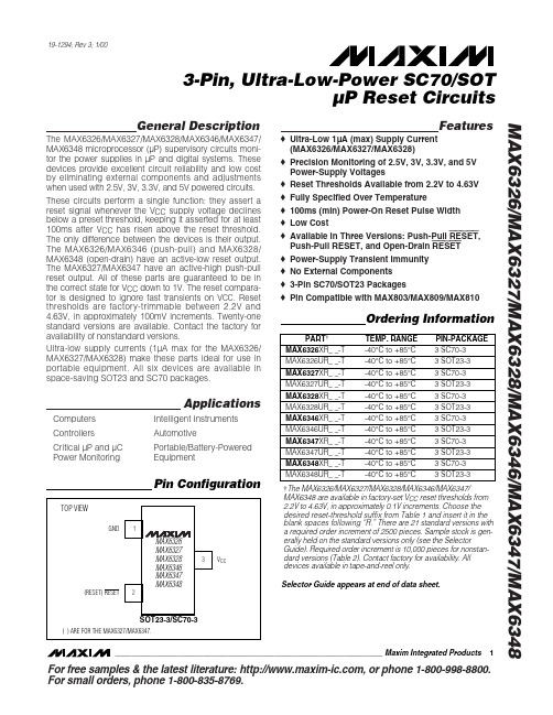
For free samples & the latest literature: , or phone 1-800-998-8800.For small orders, phone 1-800-835-8769.General DescriptionThe MAX6326/MAX6327/MAX6328/MAX6346/MAX6347/MAX6348 microprocessor (µP) supervisory circuits moni-tor the power supplies in µP and digital systems. These devices provide excellent circuit reliability and low cost by eliminating external components and adjustments when used with 2.5V, 3V, 3.3V, and 5V powered circuits.These circuits perform a single function: they assert a reset signal whenever the V CC supply voltage declines below a preset threshold, keeping it asserted for at least 100ms after V CC has risen above the reset threshold.The only difference between the devices is their output.The MAX6326/MAX6346 (push-pull) and MAX6328/MAX6348 (open-drain) have an active-low reset output.The MAX6327/MAX6347 have an active-high push-pull reset output. All of these parts are guaranteed to be in the correct state for V CC down to 1V. The reset compara-tor is designed to ignore fast transients on V CC . Reset thresholds are factory-trimmable between 2.2V and 4.63V, in approximately 100mV increments. Twenty-one standard versions are available. Contact the factory for availability of nonstandard versions.Ultra-low supply currents (1µA max for the MAX6326/MAX6327/MAX6328) make these parts ideal for use in portable equipment. All six devices are available in space-saving SOT23 and SC70 packages.ApplicationsComputers Intelligent Instruments Controllers AutomotiveCritical µP and µC Portable/Battery-Powered Power MonitoringEquipmentFeatureso Ultra-Low 1µA (max) Supply Current (MAX6326/MAX6327/MAX6328)o Precision Monitoring of 2.5V, 3V, 3.3V, and 5V Power-Supply Voltageso Reset Thresholds Available from 2.2V to 4.63V o Fully Specified Over Temperatureo 100ms (min) Power-On Reset Pulse Width o Low Costo Available in Three Versions: Push-Pull RESET ,Push-Pull RESET, and Open-Drain RESET o Power-Supply Transient Immunity o No External Componentso 3-Pin SC70/SOT23 Packageso Pin Compatible with MAX803/MAX809/MAX810MAX6326/MAX6327/MAX6328/MAX6346/MAX6347/MAX63483-Pin, Ultra-Low-Power SC70/SOTµP Reset Circuits________________________________________________________________Maxim Integrated Products 1Pin Configuration19-1294; Rev 3; 1/00†The MAX6326/MAX6327/MAX6328/MAX6346/MAX6347/MAX6348 are available in factory-set V CC reset thresholds from 2.2V to 4.63V, in approximately 0.1V increments. Choose the desired reset-threshold suffix from Table 1 and insert it in the blank spaces following “R.”There are 21 standard versions witha required order increment of 2500 pieces. Sample stock is gen-erally held on the standard versions only (see the SelectorGuide). Required order increment is 10,000 pieces for nonstan-dard versions (Table 2). Contact factory for availability. All devices available in tape-and-reel only.Selector Guide appears at end of data sheet.M A X 6326/M A X 6327/M A X 6328/M A X 6346/M A X 6347/M A X 63483-Pin, Ultra-Low-Power SC70/SOT µP Reset Circuits 2_______________________________________________________________________________________ABSOLUTE MAXIMUM RATINGSELECTRICAL CHARACTERISTICS(V CC = full range, T A = -40°C to +85°C, unless otherwise noted. Typical values are at T A = +25°C and V CC = 3V.) (Note 1)Stresses beyond those listed under “Absolute Maximum Ratings” may cause permanent damage to the device. These are stress ratings only, and functional operation of the device at these or any other conditions beyond those indicated in the operational sections of the specifications is not implied. Exposure to absolute maximum rating conditions for extended periods may affect device reliability.Terminal Voltage (with respect to GND)V CC ...........................................................................-0.3V to +6V RESET, RESET (push-pull).........................-0.3V to (V CC + 0.3V)RESET (open drain)..................................................-0.3V to +6V Input Current (V CC ).............................................................20mA Output Current (RESET, RESET ).........................................20mA Rate of Rise (V CC )...........................................................100V/µsContinuous Power Dissipation (T A = +70°C)3-Pin SC70 (derate 2.7mW/°C above +70°C)...............174mW 3-Pin SOT23 (derate 4mW/°C above +70°C)................320mW Operating Temperature Range ...........................-40°C to +85°C Storage Temperature Range.............................-65°C to +150°C Lead Temperature (soldering, 10s).................................+300°CNote 1:Overtemperature limits are guaranteed by design and not production tested.MAX6326/MAX6327/MAX6328/MAX6346/MAX6347/MAX63483-Pin, Ultra-Low-Power SC70/SOTµP Reset Circuits_______________________________________________________________________________________3__________________________________________Typical Operating Characteristics(T A = +25°C, unless otherwise noted.)00.30.20.10.40.50.60.70.80.91.0-400-2020406080SUPPLY CURRENT vs. TEMPERATURE TEMPERATURE (°C)S U P P L Y C U R R E N T(µA)050100150200-400-2020406080POWER-DOWN RESET DELAY vs. TEMPERATURE TEMPERATURE (°C)R E S E T D E L A Y(µs)130150140160170180190200210-400-2020406080POWER-UP RESET TIMEOUT vs. TEMPERATURE M A X6326-03TEMPERATURE (°C)P O W E R-U P R E S E T T I M E O U T(m s)500011001000MAXIMUM TRANSIENT DURATION vs. RESET THRESHOLD OVERDRIVE (SC70)100300400200M A X6326-04RESET THRESHOLD OVERDRIVE,V TH - V CC (mV)M A X I M U M T R A N S I E N T D U R A T I O N(µs)10______________________________________________________________Pin DescriptionM A X 6326/M A X 6327/M A X 6328/M A X 6346/M A X 6347/M A X 63483-Pin, Ultra-Low-Power SC70/SOT µP Reset Circuits 4___________________________________________________________________________________________________Applications InformationInterfacing to µPs with Bidirectional Reset PinsSince the RESET output on the MAX6328/MAX6348 is open drain, these devices interface easily with micro-processors (µPs) that have bidirectional reset pins,such as the Motorola 68HC11. Connecting the µP supervisor’s RESET output directly to the microcon-troller’s (µC’s) RESET pin with a single pull-up resistor allows either device to assert reset (Figure 1).Negative-Going V CC TransientsIn addition to issuing a reset to the µP during power-up,power-down, and brownout conditions, these devices are relatively immune to short-duration, negative-going V CC transients (glitches).The Typical Operating Characteristics show the Maxi-mum Transient Duration vs. Reset Threshold Overdrive graph, for which reset pulses are not generated. The graph shows the maximum pulse width that a negative-going V CC transient may typically have when issuing a reset signal. As the amplitude of the transient increas-es, the maximum allowable pulse width decreases.Figure 1. Interfacing to µPs with Bidirectional Reset PinsTable 1. Factory-Trimmed Reset Thresholds ‡‡Factory-trimmed reset thresholds are available in approximately 100mV increments with a 1.5% room-temperature variance.MAX6326/MAX6327/MAX6328/MAX6346/MAX6347/MAX63483-Pin, Ultra-Low-Power SC70/SOTµP Reset Circuits_______________________________________________________________________________________5Table 1. Factory-Trimmed Reset Thresholds‡(continued)‡Factory-trimmed reset thresholds are available in approximately 100mV increments with a 1.5% room-temperature variance.Table 2. Device Marking Codes and Minimum Order IncrementsM A X 6326/M A X 6327/M A X 6328/M A X 6346/M A X 6347/M A X 63483-Pin, Ultra-Low-Power SC70/SOT µP Reset Circuits 6__________________________________________________________________________________________________________Chip InformationTRANSISTOR COUNT: 419Table 2. Device Marking Codes and Minimum Order Increments (continued)Selector Guide(standard versions*)*Sample stock is generally held on all standard versions.________________________________________________________Package InformationMAX6326/MAX6327/MAX6328/MAX6346/MAX6347/MAX63483-Pin, Ultra-Low-Power SC70/SOTµP Reset Circuits_______________________________________________________________________________________7M A X 6326/M A X 6327/M A X 6328/M A X 6346/M A X 6347/M A X 63483-Pin, Ultra-Low-Power SC70/SOT µP Reset Circuits Maxim cannot assume responsibility for use of any circuitry other than circuitry entirely embodied in a Maxim product. No circuit patent licenses are implied. Maxim reserves the right to change the circuitry and specifications without notice at any time.8_____________________Maxim Integrated Products, 120 San Gabriel Drive, Sunnyvale, CA 94086 408-737-7600©2000 Maxim Integrated ProductsPrinted USAis a registered trademark of Maxim Integrated Products.Package Information (continued)。
MAX4234中文资料

PARAMETER
SYMBOL
CONDITIONS
MIN
Operating Supply Voltage Range
VDD
Inferred from PSRR test
2.7
Input Offset Voltage
VOS
Input Bias Current
IB
VCM = VSS to VDD
Input Offset Current
DC ELECTRICAL CHARACTERISTICS
(VDD = 2.7V, VSS = 0V, VCM = VDD/2, VOUT = (VDD/2), RL = ∞ connected to (VDD/2), VSHDN = VDD, TA = +25°C, unless otherwise noted.) (Note 2)
MAX4053CSE+中文资料

MAX4053CSE+中文资料General DescriptionThe MAX4051/MAX4052/MAX4053 and MAX4051A/MAX4052A/MAX4053A are low-voltage, CMOS analog ICs configured as an 8-channel multiplexer (MAX4051/A),two 4-channel multiplexers (MAX4052/A), and three sin-gle-pole/double-throw (SPDT) switches (MAX4053/A).The A-suffix parts are fully characterized for on-resistance match, on-resistance flatness, and low leakage.These CMOS devices can operate continuously with dual power supplies ranging from ±2.7V to ±8V or a single supply between +2.7V and +16V. Each switch can handle rail-to-rail analog signals. The off-leakage current is only 0.1nA at +25°C or 5nA at +85°C (MAX4051A/MAX4052A/MAX4053A).All digital inputs have 0.8V to 2.4V logic thresholds,ensuring TTL/CMOS-logic compatibility when using ±5V or a single +5V supply.________________________ApplicationsBattery-Operated Equipment Audio and Video Signal Routing Low-Voltage Data-Acquisition Systems Communications Circuits____________________________FeaturesPin Compatible with Industry-Standard74HC4051/74HC4052/74HC4053?Guaranteed On-Resistance:100?with ±5V SuppliesGuaranteed Match Between Channels:6?(MAX4051A–MAX4053A)12?(MAX4051–MAX4053)?Guaranteed Low Off-Leakage Currents:0.1nA at +25°C (MAX4051A–MAX4053A)1nA at +25°C (MAX4051–MAX4053)?Guaranteed Low On-Leakage Currents:0.1nA at +25°C (MAX4051A–MAX4053A)1nA at +25°C (MAX4051–MAX4053)?Single-Supply Operation from +2.0V to +16V Dual-Supply Operation from ±2.7V to ±8V ?TTL/CMOS-Logic Compatible ?Low Distortion: < 0.04% (600?)?Low Crosstalk: < -90dB (50?)?High Off-Isolation: < -90dB (50?)MAX4051/A, MAX4052/A, MAX4053/ALow-Voltage, CMOS AnalogMultiplexers/Switches________________________________________________________________ Maxim Integrated Products1___________________________________PinConfigurations/Functional Diagrams19-0463; Rev 2; 10/05Ordering Information continued at end of data sheet.For pricing, delivery, and ordering information,pleasecontact Maxim/Dallas Direct!at 1-888-629-4642, or visit Maxim’s website at .M A X 4051/A , M A X 4052/A , M A X 4053/ALow-Voltage, CMOS Analog Multiplexers/Switches 2___________________________________________________________________ ____________________ABSOLUTE MAXIMUM RATINGSELECTRICAL CHARACTERISTICS—Dual Supplies(V+ = +4.5V to +5.5V, V- = -4.5V to -5.5V, T A = T MIN to T MAX , unless otherwise noted. Typical values are at T A = +25°C.) Stresses beyond those listed under “Absolute Maximum Ratings” may cause permanent damage to the device. These are stress ratings only, and functional operation of the device at these or any other conditions beyond those indicated in the operational sections of the specifications is not implied. Exposure to absolute maximum rating conditions for extended periods may affect device reliability.Voltages Referenced to GNDV+........................................................................-0.3V to +17V V-..........................................................................+0.3V to -17V V+ toV-................................................................-0.3V to +17V Voltage into Any Terminal (Note 1)..........(V- - 2V) to (V+ + 2V)or 30mA (whichever occurs first)Continuous Current into Any Terminal..............................±30mA Peak Current, NO or COM(pulsed at 1ms, 10% duty cycle).................................±100mAContinuous Power Dissipation (T A = +70°C)Plastic DIP (derate 10.53m W/°C above +70°C)............842mW Narrow SO (derate 8.70mW/°C above +70°C)..............696mW QSOP (derate 8.00mW/°C above +70°C).....................640mW CERDIP (derate 10.00mW/°C above +70°C)................800mW Operating Temperature RangesMAX405_C_ E/MAX405_AC_E.............................0°C to +70°C MAX405_E_ E/MAX405_AE_E...........................-40°C to +85°C MAX405_MJE/MAX405_AMJE........................-55°C to +125°C Storage Temperature Range.............................-65°C to +150°C Lead Temperature (soldering, 10s).................................+300°CNote 1:Signals on any terminal exceeding V+ or V- are clamped by internal diodes. Limit forward-diode current to maximumcurrent rating.ELECTRICAL CHARACTERISTICS—Dual Supplies (continued) MAX4051/A, MAX4052/A, MAX4053/A Low-Voltage, CMOS Analog Multiplexers/Switches(V+ = +4.5V to +5.5V, V- = -4.5V to -5.5V, T A= T MIN to T MAX, unless otherwise noted. Typical values are at T A= +25°C.)M A X 4051/A , M A X 4052/A , M A X 4053/ALow-Voltage, CMOS Analog Multiplexers/Switches 4___________________________________________________________________ ____________________Note 2:The algebraic convention is used in this data sheet; the most negative value is shown in the minimum column.Note 3:?R ON = R ON(MAX)- R ON(MIN).Note 4:Flatness is defined as the difference between the maximum and minimum value of on-resistance as measured over thespecified analog signal ranges; i.e., V NO = 3V to 0V and 0V to -3V.Note 5:Leakage parameters are 100% tested at maximum-rated hot operating temperature, and guaranteed by correlation atT A = +25°C.Note 6:Guaranteed by design, not production tested.ELECTRICAL CHARACTERISTICS—Dual Supplies (continued) (V+ = +4.5V to +5.5V, V- = -4.5V to -5.5V, T A = T MIN to T MAX , unless otherwise noted. Typical values are at T A = +25°C.) ELECTRICAL CHARACTERISTICS—Single +5V SupplyMAX4051/A, MAX4052/A, MAX4053/A Low-Voltage, CMOS Analog Multiplexers/Switches(V+ = +4.5V to +5.5V, V- = 0V, T A= T MIN to T MAX, unless otherwise noted. Typical values are at T A= +25°C.)M A X 4051/A , M A X 4052/A , M A X 4053/ALow-Voltage, CMOS Analog Multiplexers/Switches 6___________________________________________________________________ ____________________ELECTRICAL CHARACTERISTICS—Single +5V Supply (continued)(V+ = +4.5V to +5.5V, V- = 0V, T A = T MIN to T MAX , unless otherwise noted. Typical values are at T A = +25°C.)Note 2:The algebraic convention is used in this data sheet; the most negative value is shown in the minimum column.Note 3:?R ON = R ON(MAX)- R ON(MIN).Note 4:Flatness is defined as the difference between the maximum and minimum value of on-resistance as measured over thespecified analog signal ranges; i.e., V NO = 3V to 0V and 0V to -3V.Note 5:Leakage parameters are 100% tested at maximum-rated hot operating temperature, and guaranteed by correlation atT A = +25°C.Note 6:Guaranteed by design, not production tested.ELECTRICAL CHARACTERISTICS—Single +3V SupplyMAX4051/A, MAX4052/A, MAX4053/A Low-Voltage, CMOS Analog Multiplexers/Switches(V+ = +3.0V to +3.6V, V- = 0V, T A= T MIN to T MAX, unless otherwise noted. Typical values are at T A= +25°C.)M A X 4051/A , M A X 4052/A , M A X 4053/ALow-Voltage, CMOS Analog Multiplexers/Switches 8_______________________________________________________________________________________ELECTRICAL CHARACTERISTICS—Single +3V Supply (continued)(V+ = +3.0V to +3.6V, V- = 0V, T A = T MIN to T MAX , unless otherwise noted. Typical values are at T A = +25°C.)Note 2:The algebraic convention is used in this data sheet; the most negative value is shown in the minimum column.Note 3:?R ON = R ON(MAX)- R ON(MIN).Note 4:Flatness is defined as the difference between the maximum and minimum value of on-resistance as measured over thespecified analog signal ranges; i.e., V NO = 3V to 0V and 0V to -3V.Note 5:Leakage parameters are 100% tested at maximum-rated hot operating temperature, and guaranteed by correlation atT A = +25°C.Note 6:Guaranteed by design, not production tested.MAX4051/A, MAX4052/A, MAX4053/ALow-Voltage, CMOS AnalogMultiplexers/Switches________________________________________________________________ _______________________911030-5-31ON-RESISTANCE vs. V COM(DUAL SUPPLIES)5090V COM (V)R O N (?)-13701004080605-40-22411030-5-31ON-RESISTANCE vs. V COM AND TEMPERATURE (DUAL SUPPLIES) 5090V COM (V)R O N (?)-137********605-40-2243005002ON-RESISTANCE vs. V COM (SINGLE SUPPLY)100200V COM (V)R O N (?) 4150250275225 7517512515318002ON-RESISTANCE vs. V COMAND TEMPERATURE (SINGLE SUPPLY) 100V COM (V)R O N (?)4601401601208040153-5-31CHARGE INJECTION vs. V COM-55V COM (V)Q j (p C )-135-40-2240.1OFF-LEAKAGE vs.TEMPERATURE 1000TEMPERATURE (°C)O F F -L E A K A G E (p A )101100-5012525-25075501000.1ON-LEAKAGE vs.TEMPERATURE100010,000TEMPERATURE (°C)O N -L E A K A G E (p A )101100-5012525-25075501000.1SUPPLY CURRENT vs.TEMPERATURE10TEMPERATURE (°C)I +, I - (n A )1-5012525-2507550100__________________________________________Typical Operating Characteristics(V+ = +5V, V- = -5V, GND = 0V, T A = +25°C, unlessotherwise noted.)M A X 4051/A , M A X 4052/A , M A X 4053/ALow-Voltage, CMOS Analog Multiplexers/Switches 10________________________________________________________________ __________________________________________________Typical Operating Characteristics (continued)(V+ = +5V, V- = -5V, GND = 0V, T A = +25°C, unless otherwise noted.)_____________________________________________________________Pi n Descriptions67————31, 2, 4, 5——Note:NO, NC, and COM pins are identical and interchangeable. Any may be considered an input or output; signals pass equallywell in both directions.67123515NO0B–NO3B ———MAX4052/MAX4052AMAX4053/MAX4053A0.01101001k10kTOTAL HARMONIC DISTORTIONvs. FREQUENCY0.1FREQUENCY (Hz)T H D (%)110100PIN0-10-900.010.1110100300FREQUENCY RESPONSE-80-70FREQUENCY (MHz)L O S S (d B )P H A S E (D E G R E E S )-50-60-40-20-3050-40-35-30-20-25-15-5-10INSERTION LOSS50? IN/OUT OFF-ISOLATIONON PHASE__________Applications InformationPower-Supply ConsiderationsOverviewThe MAX4051/MAX4052/MAX4053 and MAX4051A/MAX4052A/MAX4053A construction is typical of most CMOS analog switches. They have three supply pins:V+, V-,and GND. V+ and V- are used to drive the inter-nal CMOS switches and set the limits of the analog volt-age on any switch. Reverse ESD-protection diodes are internally connected between each analog signal pin and both V+ and V-. If any analog signal exceeds V+ or V-, one of these diodes will conduct. During normal operation, these (and other) reverse-biased ESD diodes leak, forming the only current drawn from V+ or V-.Virtually all the analog leakage current comes from the ESD diodes. Although the ESD diodes on a given signal pin are identical, and therefore fairly well balanced,they are reverse biased differently. Each is biased by either V+ or V- and the analog signal. This means their leakages will vary as the signal varies. The difference in the two diode leakages to the V+ and V- pins consti-tutes the analog signal path leakage current. All analog leakage current flows between each pin and one of the supply terminals, not to the other switch terminal. This is why both sides of a given switch can show leakage cur-rents of either the same or opposite polarity.There is no connection between the analog signal paths and GND.MAX4051/A, MAX4052/A, MAX4053/ALow-Voltage, CMOS AnalogMultiplexers/Switches________________________________________________________________ ______________________11Table 1. Truth Table/Switch ProgrammingX = Don’t care * ADDC not present on MAX4052.Note:NO and COM pins are identical and interchangeable. Either may be considered an input or output; signals pass equally wellin either direction.M A X 4051/A , M A X 4052/A , M A X 4053/AV+ and G ND power the internal logic and logic-level translators, and set both the input and output logic lim-its. The logic-level translators convert the logic levels into switched V+ and V- signals to drive the gates of the analog signals. This drive signal is the only connec-tion between the logic supplies (and signals) and the analog supplies. V+ and V- have ESD-protection diodes to GND.The logic-level thresholds are TTL/CMOS compatible when V+ is +5V. As V+ rises, the threshold increases slightly, so when V+ reaches +12V, the threshold is about 3.1V; above the TTL-guaranteed high-level mini-mum of 2.8V, but still compatible with CMOS outputs.Bipolar SuppliesThe se devices operate with bipolar supplies between ±3.0V and ±8V. The V+ and V- supplies need not be symmetrical, buttheir sum cannot exceed the absolute maximum rating of +17V.Single SupplyThese devices operate from a single supply between +3V and +16V when V- is connected to GND. All of the bipolar precautions must be observed. At room temper-ature, they actually “work” with a single supply at near or below +1.7V, although as supply voltage decreases,switch on-resistance and switching times become very high.Overvoltage ProtectionProper power-supply sequencing is recommended for all CMOS devices. Do not exceed the absolute maxi-mum ratings, because stresses beyond the listed rat-ings can cause permanent damage to the devices.Always sequence V+ on first, then V-, followed by the logic inputs (NO) and by COM. If power-supply sequencing is not possible, add two small signal diodes (D1, D2) in series with the supply pins for overvoltage protection (Figure 1).Adding diodes reduces the analog signal range to one diode drop below V+ and one diode drop above V-, but does not affect the devices’ low switch resistance and low leakage characteristics. Device operation is unchanged, and the difference between V+ and V-should not exceed 17V. These protection diodes are not recommended when using a single supply if signal levels must extend to ground.High-Frequency PerformanceIn 50?systems, signal response is reasonably flat up to 50MHz (see Typical Operating Characteristics ).Above 20MHz, the on response has several minor peaks which are highly layout dependent. The problem is not turning the switch on, but turning it off. The off-state switch acts like a capacitor, and passes higherfrequencies with less attenuation. At 10MHz, off isola-tion is about -45dB in 50?systems, becoming worse (approximately 20dB per decade) as frequency increases. Higher circuit impedances also make off iso-lation worse. Adjacent channel attenuation is about 3dB above that of a bare IC socket, and is entirely due to capacitive coupling.Low-Voltage, CMOS Analog Multiplexers/Switches 12__________________________________________________________________ ____________________Figure 1. Overvoltage Protection Using External Blocking DiodesMAX4051/A, MAX4052/A, MAX4053/ALow-Voltage, CMOS AnalogMultiplexers/Switches________________________________________________________________ ______________________13Figure 2. Address Transition Time______________________________________________T est Circuits/Timing DiagramsFigure 3. Enable Switching TimeM A X 4051/A , M A X 4052/A , M A X 4053/ALow-Voltage, CMOS Analog Multiplexers/Switches 14__________________________________________________________________ ____________________MAX4051/A, MAX4052/A, MAX4053/ALow-Voltage, CMOS AnalogMultiplexers/Switches________________________________________________________________ ______________________15Figure 4. Break-Before-Make Interval Figure 5. Charge InjectionM A X 4051/A , M A X 4052/A , M A X 4053/ALow-Voltage, CMOS Analog Multiplexers/Switches 16________________________________________________________________ ______________________Figure 6. Off-Isolation, On-Loss, and CrosstalkFigure 7. NO/COM CapacitanceMAX4051/A, MAX4052/A, MAX4053/ALow-Voltage, CMOS AnalogMultiplexers/Switches________________________________________________________________ ______________________17Chip InformationTRANSISTOR COUNT: 161SUBSTRATE CONNECTED TO V+.___________________________________________Ordering Information (continued)M A X 4051/A , M A X 4052/A , M A X 4053/ALow-Voltage, CMOS Analog Multiplexers/SwitchesPackage Information(The package drawing(s) in this data sheet may not reflect the most current specifications. For the latest package outline information,go to /packages .)Maxim cannot assume responsibility for use of any circuitry other than circuitry entirely embodied in a Maxim product. No circuit patent licenses are implied. Maxim reserves the right to change the circuitry and specifications without notice at any time.Maxim Integrated Products, 120 San Gabriel Drive, Sunnyvale,CA 94086 (408) 737-7600___________________19?2005 Maxim Integrated ProductsPrinted USAis a registered trademark of Maxim Integrated Products.Package Information (continued)(The package drawing(s) in this data sheet may not reflect the most current specifications. For the latest package outlineinformation,go to /packages .) MAX4051/A, MAX4052/A, MAX4053/ALow-Voltage, CMOS AnalogMultiplexers/Switches。
MAX6389XS29D4+T中文资料

General Description The MAX6381–MAX6390 microprocessor (µP) supervisory circuits monitor power-supply voltages from +1.8V to +5.0V while consuming only 3µA of supply current at +1.8V. Whenever V CC falls below the factory-set reset thresholds, the reset output asserts and remains assert-ed for a minimum reset timeout period after V CC rises above the reset threshold. Reset thresholds are available from +1.58V to +4.63V, in approximately 100mV incre-ments. Seven minimum reset timeout delays ranging from 1ms to 1200ms are available.The MAX6381/MAX6384/MAX6387 have a push-pull active-low reset output. The MAX6382/MAX6385/ MAX6388 have a push-pull active-high reset output, and the MAX6383/MAX6386/MAX6389/MAX6390 have an open-drain active-low reset output. The MAX6384/MAX6385/MAX6386 also feature a debounced manual reset input (with internal pullup resistor). The MAX6387/MAX6388/MAX6389 have an auxiliary input for monitoring a second voltage. The MAX6390 offers a manual reset input with a longer V CC reset timeout period (1120ms or 1200ms) and a shorter manual reset timeout (140ms or 150ms).The MAX6381/MAX6382/MAX6383 are available in 3-pin SC70 and6-pinµDFN packages and the MAX6384–MAX6390 are available in 4-pin SC70 andFeatures♦Factory-Set Reset Threshold Voltages Rangingfrom +1.58V to +4.63V in Approximately 100mVIncrements♦±2.5% Reset Threshold Accuracy OverTemperature (-40°C to +125°C)♦Seven Reset Timeout Periods Available: 1ms,20ms, 140ms, 280ms, 560ms, 1120ms,1200ms (min)♦3 Reset Output OptionsActive-Low Push-PullActive-High Push-PullActive-Low Open-Drain♦Reset Output State Guaranteed ValidDown to V CC= 1V♦Manual Reset Input (MAX6384/MAX6385/MAX6386)♦Auxiliary RESET IN(MAX6387/MAX6388/MAX6389)♦V CC Reset Timeout (1120ms or 1200ms)/ManualReset Timeout (140ms or 150ms) (MAX6390)♦Negative-Going V CC Transient Immunity♦Low Power Consumption of 6µA at +3.6Vand 3µA at +1.8V♦Pin Compatible withMAX809/MAX810/MAX803/MAX6326/MAX6327/MAX6328/MAX6346/MAX6347/MAX6348,and MAX6711/MAX6712/MAX6713♦Tiny 3-Pin/4-Pin SC70 and 6-Pin µDFN PackagesMAX6381–MAX6390 SC70/µDFN, Single/Dual Low-Voltage,Low-Power µP Reset Circuits ________________________________________________________________Maxim Integrated Products1Pin Configurations19-1839; Rev 4; 4/07Ordering InformationOrdering Information continued at end of data sheet.Typi cal Operati ng Ci rcui t appears at end of data sheet.Selector Guide appears at end of data sheet.after "XR", "XS", or "LT." Insert reset timeout delay (see ResetTimeout Delay table) after "D" to complete the part number.Sample stock is generally held on standard versions only (seeStandard Versions table). Standard versions have an orderincrement requirement of 2500 pieces. Nonstandard versionshave an order increment requirement of 10,000 pieces.Contact factory for availability of nonstandard versions.+Denotes a lead-free package.For pricing, delivery, and ordering information,please contact Maxim Direct at 1-888-629-4642,or visit Maxim’s website at .ComputersControllersIntelligent InstrumentsCritical µP and µCPower MonitoringPortable/Battery-Powered EquipmentDual Voltage SystemsM A X 6381–M A X 6390SC70/µDFN, Single/Dual Low-Voltage, Low-Power µP Reset CircuitsABSOLUTE MAXIMUM RATINGSELECTRICAL CHARACTERISTICS(V CC = full range, T A = -40°C to +125°C, unless otherwise specified. Typical values are at T A = +25°C.) (Note 1)Stresses beyond those listed under “Absolute Maximum Ratings” may cause permanent damage to the device. These are stress ratings only, and functional operation of the device at these or any other conditions beyond those indicated in the operational sections of the specifications is not implied. Exposure to absolute maximum rating conditions for extended periods may affect device reliability.V CC to GND..........................................................-0.3V to +6.0V RESET Open-Drain Output....................................-0.3V to +6.0V RESET , RESET (push-pull output)..............-0.3V to (V CC + 0.3V)MR , RESET IN.............................................-0.3V to (V CC + 0.3V)Input Current (V CC ).............................................................20mA Output Current (all pins).....................................................20mAContinuous Power Dissipation (T A = +70°C)3-Pin SC70 (derate 2.9mW/°C above +70°C)..............235mW 4-Pin SC70 (derate 3.1mW/°C above +70°C)..............245mW 6-Pin µDFN (derate 2.1mW/°C above +70°C)..........167.7mW Operating Temperature Range .........................-40°C to +125°C Storage Temperature Range.............................-65°C to +150°C Lead Temperature (soldering, 10s).................................+300°CMAX6381–MAX6390SC70/µDFN, Single/Dual Low-Voltage,Low-Power µP Reset Circuits_______________________________________________________________________________________3M A X 6381–M A X 6390SC70/µDFN, Single/Dual Low-Voltage, Low-Power µP Reset Circuits 4______________________________________________________________________________________Typical Operating Characteristics(T A = +25°C, unless otherwise noted.)215436789-40-105-25203550658095110125SUPPLY CURRENT vs. TEMPERATURE(NO LOAD)TEMPERATURE (°C)S U P P L Y C U R R E N T (µA )25292735333137394143-40-105-25203550658095110125POWER-DOWN RESET DELAYvs. TEMPERATURETEMPERATURE (°C)P O W E R -D O W N R E S E T D E L A Y (µs )0.940.980.961.021.001.061.041.08-40-10520-253550658095110125NORMALIZED POWER-UP RESET TIMEOUTvs. TEMPERATUREM A X 6381/90 t o c 03TEMPERATURE (°C)N O R M A L I Z E D R E S E T T I M E O U T P E R I O D0.9900.9851.0150.9950.9901.0001.0051.0101.020-40-10520-253550958011065125M A X 6381/90 t o c 04TEMPERATURE (°C)N O R M A L I Z E D R E S E T TH R E S H O L D NORMALIZED RESET THRESHOLDvs. TEMPERATURE00.40.20.80.61.01.2063912OUTPUT-VOLTAGE LOW vs. SINK CURRENTI SINK (mA)V O L (V )01.00.52.01.52.53.00500750250100012501500OUTPUT-VOLTAGE HIGH vs. SOURCE CURRENTI SOURCE (µA)V O H (V )45001100010010MAXIMUM TRANSIENT DURATION vs. RESET COMPARATOR OVERDRIVE15050350250500200100400300RESET COMPARATOR OVERDRIVE, V TH - V CC (mV)M A X I M U M T R A N S I E N T D U R A T I O N (µs )3.53.93.74.54.34.14.74.95.35.15.5-40-105-25203550658095110125RESET IN TO RESET DELAYvs. TEMPERATUREM A X 6381/90 t o c 08TEMPERATURE (°C)R E S E T I N D E L A Y (µs )MAX6381–MAX6390SC70/µDFN, Single/Dual Low-Voltage,Low-Power µP Reset CircuitsPin DescriptionM A X 6381–M A X 6390SC70/µDFN, Single/Dual Low-Voltage, Low-Power µP Reset Circuits 6_______________________________________________________________________________________Detailed DescriptionRESET OutputA µP reset input starts the µP in a known state. These µP supervisory circuits assert reset to prevent code execution errors during power-up, power-down, or brownout conditions.Reset asserts when V CC is below the reset threshold;once V CC exceeds the reset threshold, an internal timer keeps the reset output asserted for the reset timeout period. After this interval, reset output deasserts. Reset output is guaranteed to be in the correct logic state for V CC ≥1V.Manual Reset Input (MAX6384/MAX6385/MAX6386/MAX6390)Many µP-based products require manual reset capabil-ity, allowing the operator, a test technician, or external logic circuitry to initiate a reset. A logic low on MR asserts reset. Reset remains asserted while MR is low,and for the reset active timeout period (t RP ) after MR returns high. This input has an internal 63k Ωpullup resistor (1.56k Ωfor MAX6390), so it can be left uncon-nected if it is not used. MR can be driven with TTL or CMOS logic levels, or with open-drain/collector outputs.Connect a normally open momentary switch from MR to G ND to create a manual-reset function; external debounce circuitry is not required. If MR is driven from long cables or if the device is used in a noisy environ-ment, connecting a 0.1µF capacitor from MR to G ND provides additional noise immunity.RESET IN Comparator(MAX6387/MAX6388/MAX6389)RESET IN is compared to an internal +1.27V reference.If the voltage at RESET IN is less than 1.27V, reset asserts. Use the RESET IN comparator as a user-adjustable reset detector or as a secondary power-sup-ply monitor by implementing a resistor-divider at RESET IN (shown in Figure 1). Reset asserts when either V CC or RESET IN falls below its respective threshold volt-age. Use the following equation to set the threshold:V INTH = V THRST (R1/R2 + 1)where V THRST = +1.27V. To simplify the resistor selec-tion, choose a value of R2 and calculate R1:R1 = R2 [(V INTH /V THRST ) - 1]Since the input current at RESET IN is 50nA (max),large values can be used for R2 with no significant loss in accuracy.___________Applications InformationNegative-Going V CC TransientsIn addition to issuing a reset to the µP during power-up,power-down, and brownout conditions, the MAX6381–MAX6390 are relatively immune to short dura-tion negative-going V CC transients (glitches).The Typical Operating Characteristics section shows the Maximum Transient Durations vs. Reset Comparator Overdrive, for which the MAX6381–MAX6390 do not generate a reset pulse. This graph was generated usinga negative-going pulse applied to V CC , starting above the actual reset threshold and ending below it by the magnitude indicated (reset comparator overdrive). The graph indicates the typical maximum pulse width a neg-ative-going V CC transient may have without causing a reset pulse to be issued. As the magnitude of the tran-sient increases (goes farther below the reset threshold),the maximum allowable pulse width decreases. A 0.1µF capacitor mounted as close as possible to V CC provides additional transient immunity.Ensuring a Valid RESET Output Down to V CC = 0VThe MAX6381–MAX6390 are guaranteed to operate properly down to V CC = 1V. In applications that require valid reset levels down to V CC = 0V, a pulldown resistor to active-low outputs (push/pull only, Figure 2) and a pullup resistor to active-high outputs (push/pull only)will ensure that the reset line is valid while the reset out-put can no longer sink or source current. This schemedoes not work with the open-drain outputs of the MAX6383/MAX6386/MAX6389/MAX6390. The resistor value used is not critical, but it must be small enough not to load the reset output when V CC is above the reset threshold. For most applications, 100k Ωis ade-quate.MAX6381–MAX6390SC70/µDFN, Single/Dual Low-Voltage,Low-Power µP Reset Circuits_______________________________________________________________________________________7M A X 6381–M A X 6390SC70/µDFN, Single/Dual Low-Voltage, Low-Power µP Reset Circuits 8_______________________________________________________________________________________Selector GuideOrdering Information (continued)Note:Insert reset threshold suffix (see Reset Threshold table)after "XR", "XS", or "LT." Insert reset timeout delay (see Reset Timeout Delay table) after "D" to complete the part number.Sample stock is generally held on standard versions only (see Standard Versions table). Standard versions have an order increment requirement of 2500 pieces. Nonstandard versions have an order increment requirement of 10,000 pieces.Contact factory for availability of nonstandard versions.*MAX6390 is available with D4 or D7 timing only.+Denotes a lead-free package.MAX6381–MAX6390SC70/µDFN, Single/Dual Low-Voltage,Low-Power µP Reset Circuits_______________________________________________________________________________________9Chip InformationTRANSISTOR COUNT: 647PROCESS: BiCMOSPin Configurations (continued)M A X 6381–M A X 6390SC70/µDFN, Single/Dual Low-Voltage, Low-Power µP Reset Circuits 10______________________________________________________________________________________Package Information(The package drawing(s) in this data sheet may not reflect the most current specifications. For the latest package outline information,go to /packages .)MAX6381–MAX6390SC70/µDFN, Single/Dual Low-Voltage,Low-Power µP Reset Circuits______________________________________________________________________________________11Package Information (continued)(The package drawing(s) in this data sheet may not reflect the most current specifications. For the latest package outline information,go to /packages .)M A X 6381–M A X 6390SC70/µDFN, Single/Dual Low-Voltage, Low-Power µP Reset Circuits 12______________________________________________________________________________________Package Information (continued)(The package drawing(s) in this data sheet may not reflect the most current specifications. For the latest package outline information,go to /packages .)SC70/µDFN, Single/Dual Low-Voltage,Low-Power µP Reset CircuitsMaxim cannot assume responsibility for use of any circuitry other than circuitry entirely embodied in a Maxim product. No circuit patent licenses are implied. Maxim reserves the right to change the circuitry and specifications without notice at any time.Maxim Integrated Products, 120 San Gabriel Drive, Sunnyvale, CA 94086 408-737-7600____________________13©2007 Maxim Integrated Productsis a registered trademark of Maxim Integrated Products, Inc.MAX6381–MAX6390Package Information (continued)(The package drawing(s) in this data sheet may not reflect the most current specifications. For the latest package outline information,go to /packages .)Revision HistoryPages changed at Rev 4: Title on all pages, 1, 2, 5,7–13。
MAX262中文资料
M A X262中文资料(总5页) -CAL-FENGHAI.-(YICAI)-Company One1-CAL-本页仅作为文档封面,使用请直接删除在电子电路中,滤波器是不可或缺的部分,其中有源滤波器更为常用。
一般有源滤波器由运算放大器和RC元件组成,对元器件的参数精度要求比较高,设计和调试也比较麻烦。
美国Maxim公司生产的可编程滤波器芯片MAX262可以通过编程对各种低频信号实现低通、高通、带通、带阻以及全通滤波处理,且滤波的特性参数如中心频率、品质因数等,可通过编程进行设置,电路的外围器件也少。
本文介绍MAX262的情况以及由它构成的程控滤波器电路。
1 MAX262芯片介绍MAX262芯片是Maxim公司推出的双二阶通用开关电容有源滤波器,可通过微处理器精确控制滤波器的传递函数(包括设置中心频率、品质因数和工作方式)。
它采用CMOS工艺制造,在不需外部元件的情况下就可以构成各种带通、低通、高通、陷波和全通滤波器。
图1是它的引脚排列情况。
图1 MAX262引脚V+ ——正电源输入端。
V- ——负电源输入端。
GND ——模拟地。
CLKA ——外接晶体振荡器和滤波器A 部分的时钟输入端,在滤波器内部,时钟频率被2分频。
CLKB ——滤波器B 部分的时钟输入端,同样在滤波器内部,时钟频率被2分频。
CLKOUT ——晶体振荡器和R-C振荡的时钟输出端。
OSCOUT ——与晶体振荡器或R-C振荡器相连,用于自同步。
INA、INB ——滤波器的信号输入端。
BPA、BPB——带通滤波器输出端。
LPA、LPB——低通滤波器输出端。
HPA、HPB——高通、带阻、全通滤波器输出端。
WR ——写入有效输入端。
接V+时,输人数据不起作用;接V-时,数据可通过逻辑接口进入一个可编程的内存之中,以完成滤波器的工作模式、f0及Q的设置。
此外,还可以接收TTL电平信号,并上升沿锁存输人数据。
A0、A1、A2、A3 ——地址输人端,可用来完成对滤波器工作模式、f0和Q的相应设置。
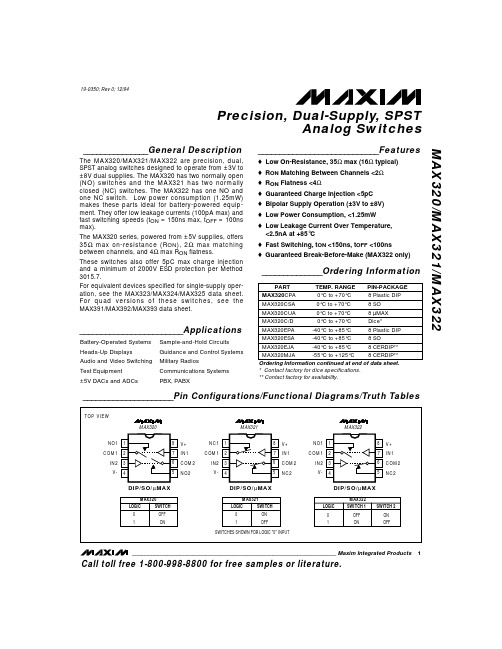
MAX320-MAX322中文资料
ELECTRICAL CHARACTERISTICS
(V+ = +5V ±10%, V- = -5V ±10%, VINH = 3.5V, VINL = 2.5V, TA = TMIN to TMAX, unless otherwise noted.)
PARAMETER ANALOG SWITCH Analog Signal Range
For equivalent devices specified for single-supply operation, see the MAX323/MAX324/MAX325 data sheet. For quad versions of these switches, see the MAX391/MAX392/MAX393 data sheet.
Plastic DIP (derate 9.09mW/°C above +70°C) .............727mW Narrow SO (derate 5.88mW/°C above +70°C) .............471mW
µMAX (derate 4.10mW/°C above +70°C) .....................330mW CERDIP (derate 8.00mW/°C above +70°C) ..................640mW Operating Temperature Ranges MAX32_C_ _ ........................................................0°C to +70°C MAX32_E_ _......................................................-40°C to +85°C MAX32_MJA ...................................................-55°C to +125°C Storage Temperature Range .............................-65°C to +150°C Lead Temperature (soldering, 10sec) .............................+300°C
MAX6362PUT23+T中文资料

For free samples and the latest literature, visit or phone 1-800-998-8800.For small orders, phone 1-800-835-8769.General DescriptionThe MAX6361–MAX6364 supervisory circuits reduce the complexity and number of components required for power-supply monitoring and battery control functions in microprocessor (µP) systems. The circuits significantly improve system reliability and accuracy compared to that obtainable with separate ICs or discrete components.Their functions include µP reset, backup battery switchover, and power failure warning.The MAX6361–MAX6364 operate from supply voltages as low as +1.2V. The factory-preset reset threshold voltage ranges from 2.32V to 4.63V (see Ordering Information ).These devices provide a manual reset input (MAX6361),watchdog timer input (MAX6362), battery-on output (MAX6363), and an auxiliary adjustable reset input (MAX6364). In addition, each part type is offered in three reset output versions: an active-low open-drain reset, an active-low open-drain reset, and an active-high open-drain reset (see Selector Guide at end of data sheet).ApplicationsFeatures♦Low +1.2V Operating Supply Voltage (V CC or V BATT )♦Precision Monitoring of +5.0V, +3.3V, +3.0V, and +2.5V Power-Supply Voltages♦Debounced Manual Reset Input (MAX6361)♦Watchdog Timer with 1.6s Timeout Period (MAX6362)♦Battery-On Output Indicator (MAX6363)♦Auxiliary User-Adjustable RESET IN (MAX6364)♦Three Available Output StructuresPush-Pull RESET , Open-Drain RESET , Open-Drain RESET♦RESET/RESET Valid Down to 1.2V Guaranteed (V CC or V BATT )♦Power-Supply Transient Immunity ♦150ms (min) Reset Timeout Period ♦Small 6-Pin SOT23 PackageMAX6361–MAX6364SOT23, Low-Power µP Supervisory Circuitswith Battery Backup________________________________________________________________Maxim Integrated Products119-1615; Rev 3; 11/05Ordering InformationPin ConfigurationsFrom the table below, select the suffix corresponding to the desired threshold voltage and insert it into the part number to complete it. When ordering from the factory, there is a 2500-piece minimum on the SOT package (tape-and-reel only).Devices are available in both leaded and lead-free packaging.Specify lead-free by replacing "-T" with "+T" when ordering.Computers ControllersIntelligent Instruments Critical µP/µC Power MonitoringFax Machines Industrial Control POS EquipmentPortable/Battery-Powered EquipmentSelector Guide appears at end of data sheet.Typical Operating Circuit appears at end of data sheet.M A X 6361–M A X 6364SOT23, Low-Power µP Supervisory Circuits with Battery BackupABSOLUTE MAXIMUM RATINGSELECTRICAL CHARACTERISTICS(V CC = +2.4V to +5.5V, V BATT = 3V, T A = -40°C to +85°C, reset not asserted. Typical values are at T A = +25°C, unless otherwise noted.) (Note 1)Stresses beyond those listed under “Absolute Maximum Ratings” may cause permanent damage to the device. These are stress ratings only, and functional operation of the device at these or any other conditions beyond those indicated in the operational sections of the specifications is not implied. Exposure to absolute maximum rating conditions for extended periods may affect device reliability.Terminal Voltages (with respect to GND)V CC , BATT, OUT.......................................................-0.3V to +6V RESET (open drain), RESET (open drain)................-0.3V to +6V BATT ON, RESET (push-pull), RESET IN,WDI.......................................................-0.3V to (V OUT + 0.3V)MR .............................................................-0.3V to (V CC + 0.3V)Input CurrentV CC Peak ............................................................................1A V CC Continuous............................................................250mA BATT Peak....................................................................250mA BATT Continuous............................................................40mAGND................................................................................75mA Output CurrentOUT................................Short-Circuit Protection for up to 10s RESET, RESET , BATT ON ..............................................20mA Continuous Power Dissipation (T A = +70°C)6-Pin SOT23 (derate 8.70mW/°C above +70°C) .........696mW Operating Temperature Range ...........................-40°C to +85°C Junction Temperature......................................................+150°C Storage Temperature Range.............................-65°C to +150°C Lead Temperature (soldering, 10s).................................+300°CMAX6361–MAX6364SOT23, Low-Power µP Supervisory Circuitswith Battery Backup_______________________________________________________________________________________3ELECTRICAL CHARACTERISTICS (continued)(V CC = +2.4V to +5.5V, V BATT = 3V, T A = -40°C to +85°C, reset not asserted. Typical values are at T A = +25°C, unless otherwise noted.) (Note 1)Note 1:All devices are 100% production tested at T A = +25°C. Limits over temperature are guaranteed by design.Note 2:V BATT can be 0 anytime or V CC can go down to 0 if V BATT is active (except at startup).M A X 6361–M A X 6364SOT23, Low-Power µP Supervisory Circuits with Battery Backup 4_______________________________________________________________________________________Typical Operating Characteristics(T A = +25°C, unless otherwise noted.)1214161820SUPPLY CURRENT vs. TEMPERATURE(NO LOAD)TEMPERATURE (°C)S U P P L Y C U R R E N T (µA )-402040-2060800.20.60.40.81.01.2BATTERY SUPPLY CURRENT (BACKUP MODE) vs. TEMPERATURETEMPERATURE (°C)B A T T E R Y S U P P L Y C U R R E N T (µA )-402040-20060801432567BATTERY TO OUT ON-RESISTANCEvs. TEMPERATURETEMPERATURE (°C)B A T T T O O U T O N -R E S I S T A NC E (Ω)-402040-20608000.30.90.61.2V CC TO OUT ON-RESISTANCEvs. TEMPERATURETEMPERATURE (°C)V O U T T O O U T O N -R E S I S T A N C E (Ω)-402040-206080190195205200210RESET TIMEOUT PERIOD vs. TEMPERATUREM A X 6361 t o c 05TEMPERATURE (°C)R E S E T T I M E O U T P E R I O D (m s )-402040-206080301575604513512010590V CC TO RESET PROPAGATION DELAYvs. TEMPERATURETEMPERATURE (°C)P R O P A G A T I O N D E LA Y (µs )-402040-2060802.03.02.55.04.54.03.5RESET THRESHOLD vs. TEMPERATURETEMPERATURE (°C)T H R E S H O L D (V )-402040-2060801.21.41.31.61.51.91.81.72.0-40-2020406080MAX6362WATCHDOG TIMEOUT PERIODvs. TEMPERATUREM A X 6361t o c 06aTEMPERATURE (°C)W A T C H D O G T I M E O U T P E R I O D (s )1100101k10kMAXIMUM TRANSIENT DURATION vs. RESET THRESHOLD OVERDRIVERESET THRESHOLD OVERDRIVE V TH - V CC (mV)M A X I M U M T R A N S I E N T D U R A T I O N (µs )400300350250200050150100MAX6361–MAX6364SOT23, Low-Power µP Supervisory Circuitswith Battery Backup1.2341.2351.236MAX6364RESET IN THRESHOLD vs. TEMPERATUREM A X 6361 t o c 10TEMPERATURE (°C)T H R E S H O L D (V )-402040-206080Typical Operating Characteristics (continued)(T A = +25°C, unless otherwise noted.)1.01.91.61.32.82.52.2MAX6364RESET IN TO RESET PROPAGATION DELAYvs. TEMPERATURETEMPERATURE (°C)P R O P A G A T I O N D E L A Y (µs )-402040-206080Pin Description0321456789101234BATTERY SUPPLY CURRENT vs. SUPPLY VOLTAGEV CC (V)B A T T E R Y S U P P L YC U R R E N T (µA )M A X 6361–M A X 6364Detailed DescriptionThe Typical Operating Circuit shows a typical connection for the MAX6361–MAX6364 family. OUT powers the stat-ic random-access memory (SRAM). OUT is internally connected to V CC if V CC is greater than the reset thresh-old, or to the greater of V CC or V BATT when V CC is less than the reset threshold. OUT can supply up to 150mA from V CC . When V CC is higher than V BATT , the BATT ON (MAX6363) output is low. When V CC is lower than V BATT ,an internal MOSF ET connects the backup battery to OUT. The on-resistance of the MOSFET is a function of backup-battery voltage and is shown in the Battery to Out On-Resistance vs. Temperature graph in the Typical Operating Characteristics section.Backup-Battery SwitchoverIn a brownout or power failure, it may be necessary to preserve the contents of the RAM. With a backup bat-tery installed at BATT, the MAX6361–MAX6364 auto-matically switch the RAM to backup power when V CC falls. The MAX6363 has a BATT ON output that goes high when in battery-backup mode. These devices require two conditions before switching to battery-backup mode:1)V CC must be below the reset threshold.2)V CC must be below V BATT .Table 1 lists the status of the inputs and outputs in bat-tery-backup mode. The device will not power up if the only voltage source is on BATT. OUT will only power up from V CC at startup.Manual Reset Input (MAX6361 Only)Many µP-based products require manual reset capabili-ty, allowing the operator, a test technician, or external logic circuitry to initiate a reset. For the MAX6361, a logic low on MR asserts reset. Reset remains asserted while MR is low, and for a minimum of 150ms (t RP ) after it returns high. MR has an internal 20k Ωpull-up resistor to V CC . This input can be driven with TTL/CMOS logic lev-els or with open-drain/collector outputs. Connect a nor-mally open momentary switch from MR to GND to create a manual reset function; external debounce circuitry is not required. If MR is driven from long cables or the device is used in a noisy environment, connect a 0.1µF capacitor from MR to GND to provide additional noise immunity.Watchdog Input (MAX6362 Only)The watchdog monitors µP activity through the input WDI. If the µP becomes inactive, the reset output is asserted in pulses. To use the watchdog function, con-nect WDI to a bus line or µP I/O line. A change of state(high to low or low to high) within the watchdog timeout period (t WD ) with a 100ns minimum pulse width clears the watchdog timer. If WDI remains high or low for longer than the watchdog timeout period, the internal watchdog timer runs out and a reset pulse is triggered for the reset timeout period (t RP ). The internal watchdog timer clears whenever reset asserts or the WDI sees a rising or falling edge within the watchdog timeout period. If WDI remains in a high or low state for an extended period of time, a reset pulse asserts after every watchdog timeout period (t WD ) (Figure 1).Reset In (MAX6364 Only)RESET IN is compared to an internal 1.235V reference.If the voltage at RESET IN is less than 1.235V, reset is asserted. The RESET IN comparator may be used as an undervoltage detector to signal a failing power sup-ply. It can also be used as a secondary power-supply reset monitor.To program the reset threshold (V RTH ) of the secondary power supply, use the following equation (see Typical Operating Circuit ):where V REF = 1.235V. To simplify the resistor selection,choose a value for R2 and calculate R1:Since the input current at RESET IN is 25nA (max), large values (up to 1M Ω) can be used for R2 with no signifi-cant loss in accuracy. F or example, in the TypicalSOT23, Low-Power µP Supervisory Circuits with Battery Backup 6_______________________________________________________________________________________R R V V RTH REF 121 /=()−[]MAX6361–MAX6364SOT23, Low-Power µP Supervisory Circuitswith Battery Backup_______________________________________________________________________________________7Operating Circuit,the MAX6362 monitors two supply voltages. To monitor the secondary 5V logic or analog supply with a 4.60V nominal programmed reset thresh-old, choose R2 = 100k Ω, and calculate R1 = 273k Ω.Reset OutputA µP’s reset input starts the µP in a known state. The MAX6361–MAX6364 µP supervisory circuits assert a reset to prevent code-execution errors during power-up, power-down, and brownout conditions. RESET is guaranteed to be a logic low or high depending on the device chosen (see Ordering Information ). RESET or RESET asserts when V CC is below the reset threshold and for at least 150ms (t RP ) after V CC rises above the reset threshold. RESET or RESET also asserts when MR is low (MAX6361) and when RESET IN is less than 1.235V (MAX6364). The MAX6362 watchdog function will cause RESET (or RESET ) to assert in pulses follow-ing a watchdog timeout (Figure 1).Applications InformationOperation Without a BackupPower SourceThe MAX6361–MAX6364 were designed for battery-backed applications. If a backup battery is not used,connect V CC to OUT and connect BATT to GND.Replacing the Backup BatteryIf BATT is decoupled with a 0.1µF capacitor to ground,the backup power source can be removed while V CC remains valid without danger of triggering a reset pulse.The device does not enter battery-backup mode when V CC stays above the reset threshold voltage.Negative-Going V CC TransientsThese supervisors are relatively immune to short-dura-tion, negative-going V CC transients. Resetting the µPwhen V CC experiences only small glitches is usually not desirable.The Typical Operating Characteristics section shows a graph of Maximum Transient Duration vs. Reset Threshold Overdrive for which reset is not asserted.The graph was produced using negative-going V CC pulses, starting at V CC and ending below the reset threshold by the magnitude indicated (reset threshold overdrive). The graph shows the maximum pulse width that a negative-going V CC transient can typically have without triggering a reset pulse. As the amplitude of the transient increases (i.e., goes further below the reset threshold), the maximum allowable pulse width decreases. Typically, a V CC transient that goes 100mV below the reset threshold and lasts for 30µs will not trigger a reset pulse.A 0.1µF bypass capacitor mounted close to the V CC pin provides additional transient immunity.Figure 1. MAX6362 Watchdog Timeout Period and Reset Active TimeM A X 6361–M A X 6364Watchdog Software Considerations(MAX6362 Only)To help the watchdog timer monitor software execution more closely, set and reset the watchdog input at dif-ferent points in the program, rather than “pulsing” the watchdog input low-high-low. This technique avoids a “stuck” loop, in which the watchdog timer would contin-ue to be reset within the loop, keeping the watchdog from timing out. F igure 2 shows an example of a flow diagram where the I/O driving the WDI is set low at the beginning of the program, set high at the beginning of every subroutine or loop, then set low again when the program returns to the beginning. If the program should “hang” in any subroutine, the problem would quickly be corrected, since the I/O is continually set low and the watchdog timer is allowed to time out, trigger-ing a reset.SOT23, Low-Power µP Supervisory Circuits with Battery Backup 8_______________________________________________________________________________________Figure 2. Watchdog Flow DiagramMAX6361–MAX6364SOT23, Low-Power µP Supervisory Circuitswith Battery Backup_______________________________________________________________________________________9*Sample stock generally held on standard versions only. Contact factory for availability of nonstandard versions.Device Marking CodesSelector GuideM A X 6361–M A X 6364SOT23, Low-Power µP Supervisory Circuits with Battery Backup 10______________________________________________________________________________________Pin Configurations (continued)Typical Operating CircuitChip InformationTRANSISTOR COUNT: 720MAX6361–MAX6364SOT23, Low-Power µP Supervisory Circuits with Battery Backup______________________________________________________________________________________11Package InformationM A X 6361–M A X 6364SOT23, Low-Power µP Supervisory Circuits with Battery BackupMaxim cannot assume responsibility for use of any circuitry other than circuitry entirely embodied in a Maxim product. No circuit patent licenses are implied. Maxim reserves the right to change the circuitry and specifications without notice at any time.12____________________Maxim Integrated Products, 120 San Gabriel Drive, Sunnyvale, CA 94086 408-737-7600©2005 Maxim Integrated Products Printed USA is a registered trademark of Maxim Integrated Products, Inc.NOTES。
MAX6412UK28+中文资料

Continuous Power Dissipation (TA = +70°C) 5-Pin SOT23-5 (derate 7.1mW/°C above +70°C) ........571mW
Operating Temperature Range .........................-40°C to +125°C Junction Temperature ......................................................+150°C Storage Temperature Range .............................-65°C to +150°C Lead Temperature (soldering, 10s) .................................+300°C
TEMP RANGE -40°C to +125°C -40°C to +125°C -40°C to +125°C -40°C to +125°C -40°C to +125°C -40°C to +125°C -40°C to +125°C -40°C to +125°C -40°C to +125°C
♦ Guaranteed Reset Valid to VCC = 1V ♦ Power-Supply Transient Immunity
♦ Small SOT23-5 Packages
Ordering Information
PART MAX6412UK_ _-T MAX6413UK_ _-T MAX6414UK_ _-T MAX6415UK-T MAX64168UK_ _-T MAX6419UK_ _-T MAX6420UK_ _-T
- 1、下载文档前请自行甄别文档内容的完整性,平台不提供额外的编辑、内容补充、找答案等附加服务。
- 2、"仅部分预览"的文档,不可在线预览部分如存在完整性等问题,可反馈申请退款(可完整预览的文档不适用该条件!)。
- 3、如文档侵犯您的权益,请联系客服反馈,我们会尽快为您处理(人工客服工作时间:9:00-18:30)。
For free samples and the latest literature, visit or phone 1-800-998-8800.For small orders, phone 1-800-835-8769.General DescriptionThe MAX6361–MAX6364 supervisory circuits reduce the complexity and number of components required for power-supply monitoring and battery control functions in microprocessor (µP) systems. The circuits significantly improve system reliability and accuracy compared to that obtainable with separate ICs or discrete components.Their functions include µP reset, backup battery switchover, and power failure warning.The MAX6361–MAX6364 operate from supply voltages as low as +1.2V. The factory-preset reset threshold voltage ranges from 2.32V to 4.63V (see Ordering Information ).These devices provide a manual reset input (MAX6361),watchdog timer input (MAX6362), battery-on output (MAX6363), and an auxiliary adjustable reset input (MAX6364). In addition, each part type is offered in three reset output versions: an active-low open-drain reset, an active-low open-drain reset, and an active-high open-drain reset (see Selector Guide at end of data sheet).ApplicationsFeatures♦Low +1.2V Operating Supply Voltage (V CC or V BATT )♦Precision Monitoring of +5.0V, +3.3V, +3.0V, and +2.5V Power-Supply Voltages♦Debounced Manual Reset Input (MAX6361)♦Watchdog Timer with 1.6s Timeout Period (MAX6362)♦Battery-On Output Indicator (MAX6363)♦Auxiliary User-Adjustable RESET IN (MAX6364)♦Three Available Output StructuresPush-Pull RESET , Open-Drain RESET , Open-Drain RESET♦RESET/RESET Valid Down to 1.2V Guaranteed (V CC or V BATT )♦Power-Supply Transient Immunity ♦150ms (min) Reset Timeout Period ♦Small 6-Pin SOT23 PackageMAX6361–MAX6364SOT23, Low-Power µP Supervisory Circuitswith Battery Backup________________________________________________________________Maxim Integrated Products119-1615; Rev 3; 11/05Ordering InformationPin ConfigurationsFrom the table below, select the suffix corresponding to the desired threshold voltage and insert it into the part number to complete it. When ordering from the factory, there is a 2500-piece minimum on the SOT package (tape-and-reel only).Devices are available in both leaded and lead-free packaging.Specify lead-free by replacing "-T" with "+T" when ordering.Computers ControllersIntelligent Instruments Critical µP/µC Power MonitoringFax Machines Industrial Control POS EquipmentPortable/Battery-Powered EquipmentSelector Guide appears at end of data sheet.Typical Operating Circuit appears at end of data sheet.M A X 6361–M A X 6364SOT23, Low-Power µP Supervisory Circuits with Battery BackupABSOLUTE MAXIMUM RATINGSELECTRICAL CHARACTERISTICS(V CC = +2.4V to +5.5V, V BATT = 3V, T A = -40°C to +85°C, reset not asserted. Typical values are at T A = +25°C, unless otherwise noted.) (Note 1)Stresses beyond those listed under “Absolute Maximum Ratings” may cause permanent damage to the device. These are stress ratings only, and functional operation of the device at these or any other conditions beyond those indicated in the operational sections of the specifications is not implied. Exposure to absolute maximum rating conditions for extended periods may affect device reliability.Terminal Voltages (with respect to GND)V CC , BATT, OUT.......................................................-0.3V to +6V RESET (open drain), RESET (open drain)................-0.3V to +6V BATT ON, RESET (push-pull), RESET IN,WDI.......................................................-0.3V to (V OUT + 0.3V)MR .............................................................-0.3V to (V CC + 0.3V)Input CurrentV CC Peak ............................................................................1A V CC Continuous............................................................250mA BATT Peak....................................................................250mA BATT Continuous............................................................40mAGND................................................................................75mA Output CurrentOUT................................Short-Circuit Protection for up to 10s RESET, RESET , BATT ON ..............................................20mA Continuous Power Dissipation (T A = +70°C)6-Pin SOT23 (derate 8.70mW/°C above +70°C) .........696mW Operating Temperature Range ...........................-40°C to +85°C Junction Temperature......................................................+150°C Storage Temperature Range.............................-65°C to +150°C Lead Temperature (soldering, 10s).................................+300°CMAX6361–MAX6364SOT23, Low-Power µP Supervisory Circuitswith Battery Backup_______________________________________________________________________________________3ELECTRICAL CHARACTERISTICS (continued)(V CC = +2.4V to +5.5V, V BATT = 3V, T A = -40°C to +85°C, reset not asserted. Typical values are at T A = +25°C, unless otherwise noted.) (Note 1)Note 1:All devices are 100% production tested at T A = +25°C. Limits over temperature are guaranteed by design.Note 2:V BATT can be 0 anytime or V CC can go down to 0 if V BATT is active (except at startup).M A X 6361–M A X 6364SOT23, Low-Power µP Supervisory Circuits with Battery Backup 4_______________________________________________________________________________________Typical Operating Characteristics(T A = +25°C, unless otherwise noted.)1214161820SUPPLY CURRENT vs. TEMPERATURE(NO LOAD)TEMPERATURE (°C)S U P P L Y C U R R E N T (µA )-402040-2060800.20.60.40.81.01.2BATTERY SUPPLY CURRENT (BACKUP MODE) vs. TEMPERATURETEMPERATURE (°C)B A T T E R Y S U P P L Y C U R R E N T (µA )-402040-20060801432567BATTERY TO OUT ON-RESISTANCEvs. TEMPERATURETEMPERATURE (°C)B A T T T O O U T O N -R E S I S T A NC E (Ω)-402040-20608000.30.90.61.2V CC TO OUT ON-RESISTANCEvs. TEMPERATURETEMPERATURE (°C)V O U T T O O U T O N -R E S I S T A N C E (Ω)-402040-206080190195205200210RESET TIMEOUT PERIOD vs. TEMPERATUREM A X 6361 t o c 05TEMPERATURE (°C)R E S E T T I M E O U T P E R I O D (m s )-402040-206080301575604513512010590V CC TO RESET PROPAGATION DELAYvs. TEMPERATURETEMPERATURE (°C)P R O P A G A T I O N D E LA Y (µs )-402040-2060802.03.02.55.04.54.03.5RESET THRESHOLD vs. TEMPERATURETEMPERATURE (°C)T H R E S H O L D (V )-402040-2060801.21.41.31.61.51.91.81.72.0-40-2020406080MAX6362WATCHDOG TIMEOUT PERIODvs. TEMPERATUREM A X 6361t o c 06aTEMPERATURE (°C)W A T C H D O G T I M E O U T P E R I O D (s )1100101k10kMAXIMUM TRANSIENT DURATION vs. RESET THRESHOLD OVERDRIVERESET THRESHOLD OVERDRIVE V TH - V CC (mV)M A X I M U M T R A N S I E N T D U R A T I O N (µs )400300350250200050150100MAX6361–MAX6364SOT23, Low-Power µP Supervisory Circuitswith Battery Backup1.2341.2351.236MAX6364RESET IN THRESHOLD vs. TEMPERATUREM A X 6361 t o c 10TEMPERATURE (°C)T H R E S H O L D (V )-402040-206080Typical Operating Characteristics (continued)(T A = +25°C, unless otherwise noted.)1.01.91.61.32.82.52.2MAX6364RESET IN TO RESET PROPAGATION DELAYvs. TEMPERATURETEMPERATURE (°C)P R O P A G A T I O N D E L A Y (µs )-402040-206080Pin Description0321456789101234BATTERY SUPPLY CURRENT vs. SUPPLY VOLTAGEV CC (V)B A T T E R Y S U P P L YC U R R E N T (µA )M A X 6361–M A X 6364Detailed DescriptionThe Typical Operating Circuit shows a typical connection for the MAX6361–MAX6364 family. OUT powers the stat-ic random-access memory (SRAM). OUT is internally connected to V CC if V CC is greater than the reset thresh-old, or to the greater of V CC or V BATT when V CC is less than the reset threshold. OUT can supply up to 150mA from V CC . When V CC is higher than V BATT , the BATT ON (MAX6363) output is low. When V CC is lower than V BATT ,an internal MOSF ET connects the backup battery to OUT. The on-resistance of the MOSFET is a function of backup-battery voltage and is shown in the Battery to Out On-Resistance vs. Temperature graph in the Typical Operating Characteristics section.Backup-Battery SwitchoverIn a brownout or power failure, it may be necessary to preserve the contents of the RAM. With a backup bat-tery installed at BATT, the MAX6361–MAX6364 auto-matically switch the RAM to backup power when V CC falls. The MAX6363 has a BATT ON output that goes high when in battery-backup mode. These devices require two conditions before switching to battery-backup mode:1)V CC must be below the reset threshold.2)V CC must be below V BATT .Table 1 lists the status of the inputs and outputs in bat-tery-backup mode. The device will not power up if the only voltage source is on BATT. OUT will only power up from V CC at startup.Manual Reset Input (MAX6361 Only)Many µP-based products require manual reset capabili-ty, allowing the operator, a test technician, or external logic circuitry to initiate a reset. For the MAX6361, a logic low on MR asserts reset. Reset remains asserted while MR is low, and for a minimum of 150ms (t RP ) after it returns high. MR has an internal 20k Ωpull-up resistor to V CC . This input can be driven with TTL/CMOS logic lev-els or with open-drain/collector outputs. Connect a nor-mally open momentary switch from MR to GND to create a manual reset function; external debounce circuitry is not required. If MR is driven from long cables or the device is used in a noisy environment, connect a 0.1µF capacitor from MR to GND to provide additional noise immunity.Watchdog Input (MAX6362 Only)The watchdog monitors µP activity through the input WDI. If the µP becomes inactive, the reset output is asserted in pulses. To use the watchdog function, con-nect WDI to a bus line or µP I/O line. A change of state(high to low or low to high) within the watchdog timeout period (t WD ) with a 100ns minimum pulse width clears the watchdog timer. If WDI remains high or low for longer than the watchdog timeout period, the internal watchdog timer runs out and a reset pulse is triggered for the reset timeout period (t RP ). The internal watchdog timer clears whenever reset asserts or the WDI sees a rising or falling edge within the watchdog timeout period. If WDI remains in a high or low state for an extended period of time, a reset pulse asserts after every watchdog timeout period (t WD ) (Figure 1).Reset In (MAX6364 Only)RESET IN is compared to an internal 1.235V reference.If the voltage at RESET IN is less than 1.235V, reset is asserted. The RESET IN comparator may be used as an undervoltage detector to signal a failing power sup-ply. It can also be used as a secondary power-supply reset monitor.To program the reset threshold (V RTH ) of the secondary power supply, use the following equation (see Typical Operating Circuit ):where V REF = 1.235V. To simplify the resistor selection,choose a value for R2 and calculate R1:Since the input current at RESET IN is 25nA (max), large values (up to 1M Ω) can be used for R2 with no signifi-cant loss in accuracy. F or example, in the TypicalSOT23, Low-Power µP Supervisory Circuits with Battery Backup 6_______________________________________________________________________________________R R V V RTH REF 121 /=()−[]MAX6361–MAX6364SOT23, Low-Power µP Supervisory Circuitswith Battery Backup_______________________________________________________________________________________7Operating Circuit,the MAX6362 monitors two supply voltages. To monitor the secondary 5V logic or analog supply with a 4.60V nominal programmed reset thresh-old, choose R2 = 100k Ω, and calculate R1 = 273k Ω.Reset OutputA µP’s reset input starts the µP in a known state. The MAX6361–MAX6364 µP supervisory circuits assert a reset to prevent code-execution errors during power-up, power-down, and brownout conditions. RESET is guaranteed to be a logic low or high depending on the device chosen (see Ordering Information ). RESET or RESET asserts when V CC is below the reset threshold and for at least 150ms (t RP ) after V CC rises above the reset threshold. RESET or RESET also asserts when MR is low (MAX6361) and when RESET IN is less than 1.235V (MAX6364). The MAX6362 watchdog function will cause RESET (or RESET ) to assert in pulses follow-ing a watchdog timeout (Figure 1).Applications InformationOperation Without a BackupPower SourceThe MAX6361–MAX6364 were designed for battery-backed applications. If a backup battery is not used,connect V CC to OUT and connect BATT to GND.Replacing the Backup BatteryIf BATT is decoupled with a 0.1µF capacitor to ground,the backup power source can be removed while V CC remains valid without danger of triggering a reset pulse.The device does not enter battery-backup mode when V CC stays above the reset threshold voltage.Negative-Going V CC TransientsThese supervisors are relatively immune to short-dura-tion, negative-going V CC transients. Resetting the µPwhen V CC experiences only small glitches is usually not desirable.The Typical Operating Characteristics section shows a graph of Maximum Transient Duration vs. Reset Threshold Overdrive for which reset is not asserted.The graph was produced using negative-going V CC pulses, starting at V CC and ending below the reset threshold by the magnitude indicated (reset threshold overdrive). The graph shows the maximum pulse width that a negative-going V CC transient can typically have without triggering a reset pulse. As the amplitude of the transient increases (i.e., goes further below the reset threshold), the maximum allowable pulse width decreases. Typically, a V CC transient that goes 100mV below the reset threshold and lasts for 30µs will not trigger a reset pulse.A 0.1µF bypass capacitor mounted close to the V CC pin provides additional transient immunity.Figure 1. MAX6362 Watchdog Timeout Period and Reset Active TimeM A X 6361–M A X 6364Watchdog Software Considerations(MAX6362 Only)To help the watchdog timer monitor software execution more closely, set and reset the watchdog input at dif-ferent points in the program, rather than “pulsing” the watchdog input low-high-low. This technique avoids a “stuck” loop, in which the watchdog timer would contin-ue to be reset within the loop, keeping the watchdog from timing out. F igure 2 shows an example of a flow diagram where the I/O driving the WDI is set low at the beginning of the program, set high at the beginning of every subroutine or loop, then set low again when the program returns to the beginning. If the program should “hang” in any subroutine, the problem would quickly be corrected, since the I/O is continually set low and the watchdog timer is allowed to time out, trigger-ing a reset.SOT23, Low-Power µP Supervisory Circuits with Battery Backup 8_______________________________________________________________________________________Figure 2. Watchdog Flow DiagramMAX6361–MAX6364SOT23, Low-Power µP Supervisory Circuitswith Battery Backup_______________________________________________________________________________________9*Sample stock generally held on standard versions only. Contact factory for availability of nonstandard versions.Device Marking CodesSelector GuideM A X 6361–M A X 6364SOT23, Low-Power µP Supervisory Circuits with Battery Backup 10______________________________________________________________________________________Pin Configurations (continued)Typical Operating CircuitChip InformationTRANSISTOR COUNT: 720MAX6361–MAX6364SOT23, Low-Power µP Supervisory Circuits with Battery Backup______________________________________________________________________________________11Package InformationM A X 6361–M A X 6364SOT23, Low-Power µP Supervisory Circuits with Battery BackupMaxim cannot assume responsibility for use of any circuitry other than circuitry entirely embodied in a Maxim product. No circuit patent licenses are implied. Maxim reserves the right to change the circuitry and specifications without notice at any time.12____________________Maxim Integrated Products, 120 San Gabriel Drive, Sunnyvale, CA 94086 408-737-7600©2005 Maxim Integrated Products Printed USA is a registered trademark of Maxim Integrated Products, Inc.NOTES。