MAX1147BCUP中文资料
MAX13085EESA-T中文资料

General DescriptionThe MAX13080E–MAX13089E +5.0V, ±15kV ESD-protect-ed, RS-485/RS-422 transceivers feature one driver and one receiver. These devices include fail-safe circuitry,guaranteeing a logic-high receiver output when receiver inputs are open or shorted. The receiver outputs a logic-high if all transmitters on a terminated bus are disabled (high impedance). The MAX13080E–MAX13089E include a hot-swap capability to eliminate false transitions on the bus during power-up or hot insertion.The MAX13080E/MAX13081E/MAX13082E feature reduced slew-rate drivers that minimize EMI and reduce reflections caused by improperly terminated cables, allowing error-free data transmission up to 250kbps. The MAX13083E/MAX13084E/MAX13085E also feature slew-rate-limited drivers but allow transmit speeds up to 500kbps. The MAX13086E/MAX13087E/MAX13088E driver slew rates are not limited, making transmit speeds up to 16Mbps possible. The MAX13089E slew rate is pin selectable for 250kbps,500kbps, and 16Mbps.The MAX13082E/MAX13085E/MAX13088E are intended for half-duplex communications, and the MAX13080E/MAX13081E/MAX13083E/MAX13084E/MAX13086E/MAX13087E are intended for full-duplex communica-tions. The MAX13089E is selectable for half-duplex or full-duplex operation. It also features independently programmable receiver and transmitter output phase through separate pins.The MAX13080E–MAX13089E transceivers draw 1.2mA of supply current when unloaded or when fully loaded with the drivers disabled. All devices have a 1/8-unit load receiver input impedance, allowing up to 256transceivers on the bus.The MAX13080E/MAX13083E/MAX13086E/MAX13089E are available in 14-pin PDIP and 14-pin SO packages.The MAX13081E/MAX13082E/MAX13084E/MAX13085E/MAX13087E/MAX13088E are available in 8-pin PDIP and 8-pin SO packages. The devices operate over the com-mercial, extended, and automotive temperature ranges.ApplicationsUtility Meters Lighting Systems Industrial Control Telecom Security Systems Instrumentation ProfibusFeatures♦+5.0V Operation♦Extended ESD Protection for RS-485/RS-422 I/O Pins±15kV Human Body Model ♦True Fail-Safe Receiver While Maintaining EIA/TIA-485 Compatibility ♦Hot-Swap Input Structures on DE and RE ♦Enhanced Slew-Rate Limiting Facilitates Error-Free Data Transmission(MAX13080E–MAX13085E/MAX13089E)♦Low-Current Shutdown Mode (Except MAX13081E/MAX13084E/MAX13087E)♦Pin-Selectable Full-/Half-Duplex Operation (MAX13089E)♦Phase Controls to Correct for Twisted-Pair Reversal (MAX13089E)♦Allow Up to 256 Transceivers on the Bus ♦Available in Industry-Standard 8-Pin SO PackageMAX13080E–MAX13089E+5.0V , ±15kV ESD-Protected, Fail-Safe, Hot-Swap, RS-485/RS-422 Transceivers________________________________________________________________Maxim Integrated Products 1Ordering Information19-3590; Rev 1; 4/05For pricing, delivery, and ordering information,please contact Maxim/Dallas Direct!at 1-888-629-4642, or visit Maxim’s website at .Selector Guide, Pin Configurations, and Typical Operating Circuits appear at end of data sheet.Ordering Information continued at end of data sheet.M A X 13080E –M A X 13089E+5.0V , ±15kV ESD-Protected, Fail-Safe, Hot-Swap, RS-485/RS-422 Transceivers 2_______________________________________________________________________________________ABSOLUTE MAXIMUM RATINGSDC ELECTRICAL CHARACTERISTICS(V CC = +5.0V ±10%, T A = T MIN to T MAX , unless otherwise noted. Typical values are at V CC = +5.0V and T A = +25°C.) (Note 1)Stresses beyond those listed under “Absolute Maximum Ratings” may cause permanent damage to the device. These are stress ratings only, and functional operation of the device at these or any other conditions beyond those indicated in the operational sections of the specifications is not implied. Exposure to absolute maximum rating conditions for extended periods may affect device reliability.(All Voltages Referenced to GND)Supply Voltage (V CC ).............................................................+6V Control Input Voltage (RE , DE, SLR,H/F , TXP, RXP)......................................................-0.3V to +6V Driver Input Voltage (DI)...........................................-0.3V to +6V Driver Output Voltage (Z, Y, A, B).............................-8V to +13V Receiver Input Voltage (A, B)....................................-8V to +13V Receiver Input VoltageFull Duplex (A, B)..................................................-8V to +13V Receiver Output Voltage (RO)....................-0.3V to (V CC + 0.3V)Driver Output Current.....................................................±250mAContinuous Power Dissipation (T A = +70°C)8-Pin SO (derate 5.88mW/°C above +70°C).................471mW 8-Pin Plastic DIP (derate 9.09mW/°C above +70°C).....727mW 14-Pin SO (derate 8.33mW/°C above +70°C)...............667mW 14-Pin Plastic DIP (derate 10.0mW/°C above +70°C)...800mW Operating Temperature RangesMAX1308_EC_ _.................................................0°C to +75°C MAX1308_EE_ _..............................................-40°C to +85°C MAX1308_EA_ _............................................-40°C to +125°C Junction Temperature......................................................+150°C Storage Temperature Range.............................-65°C to +150°C Lead Temperature (soldering, 10s).................................+300°CMAX13080E–MAX13089E+5.0V , ±15kV ESD-Protected, Fail-Safe, Hot-Swap, RS-485/RS-422 Transceivers_______________________________________________________________________________________3DC ELECTRICAL CHARACTERISTICS (continued)(V CC = +5.0V ±10%, T A = T MIN to T MAX , unless otherwise noted. Typical values are at V CC = +5.0V and T A = +25°C.) (Note 1)M A X 13080E –M A X 13089E+5.0V , ±15kV ESD-Protected, Fail-Safe, Hot-Swap, RS-485/RS-422 Transceivers 4_______________________________________________________________________________________DRIVER SWITCHING CHARACTERISTICSMAX13080E/MAX13081E/MAX13082E/MAX13089E WITH SRL = UNCONNECTED (250kbps)(V CC = +5.0V ±10%, T A = T MIN to T MAX , unless otherwise noted. Typical values are at V CC = +5.0V and T A = +25°C.)RECEIVER SWITCHING CHARACTERISTICSMAX13080E/MAX13081E/MAX13082E/MAX13089E WITH SRL = UNCONNECTED (250kbps)(V CC = +5.0V ±10%, T A = T MIN to T MAX , unless otherwise noted. Typical values are at V CC = +5.0V and T A = +25°C.)MAX13080E–MAX13089E+5.0V , ±15kV ESD-Protected, Fail-Safe, Hot-Swap, RS-485/RS-422 Transceivers_______________________________________________________________________________________5DRIVER SWITCHING CHARACTERISTICSMAX13083E/MAX13084E/MAX13085E/MAX13089E WITH SRL = V CC (500kbps)(V CC = +5.0V ±10%, T A = T MIN to T MAX , unless otherwise noted. Typical values are at V CC = +5.0V and T A = +25°C.)RECEIVER SWITCHING CHARACTERISTICSMAX13083E/MAX13084E/MAX13085E/MAX13089E WITH SRL = V CC (500kbps)(V CC = +5.0V ±10%, T A = T MIN to T MAX , unless otherwise noted. Typical values are at V CC = +5.0V and T A = +25°C.)M A X 13080E –M A X 13089E+5.0V , ±15kV ESD-Protected, Fail-Safe, Hot-Swap, RS-485/RS-422 Transceivers 6_______________________________________________________________________________________DRIVER SWITCHING CHARACTERISTICSMAX13086E/MAX13087E/MAX13088E/MAX13089E WITH SRL = GND (16Mbps)(V CC = +5.0V ±10%, T A = T MIN to T MAX , unless otherwise noted. Typical values are at V CC = +5.0V and T A = +25°C.)RECEIVER SWITCHING CHARACTERISTICSMAX13086E/MAX13087E/MAX13088E/MAX13089E WITH SRL = GND (16Mbps)(V CC = +5.0V ±10%, T A = T MIN to T MAX , unless otherwise noted. Typical values are at V CC = +5.0V and T A = +25°C.)Note 2:∆V OD and ∆V OC are the changes in V OD and V OC , respectively, when the DI input changes state.Note 3:The short-circuit output current applies to peak current just prior to foldback current limiting. The short-circuit foldback outputcurrent applies during current limiting to allow a recovery from bus contention.MAX13080E–MAX13089E+5.0V , ±15kV ESD-Protected, Fail-Safe, Hot-Swap, RS-485/RS-422 Transceivers_______________________________________________________________________________________70.800.901.501.101.001.201.301.401.60-40-10520-253550958011065125SUPPLY CURRENT vs. TEMPERATURETEMPERATURE (°C)S U P P L Y C U R R E N T (m A )0201040305060021345OUTPUT CURRENTvs. RECEIVER OUTPUT-HIGH VOLTAGEM A X 13080E -89E t o c 02OUTPUT HIGH VOLTAGE (V)O U T P U T C U R R E N T (m A )20104030605070021345OUTPUT CURRENTvs. RECEIVER OUTPUT-LOW VOLTAGEM A X 13080E -89E t o c 03OUTPUT LOW VOLTAGE (V)O U T P U T C U R R E N T (m A )4.04.44.24.84.65.25.05.4RECEIVER OUTPUT-HIGH VOLTAGEvs. TEMPERATURETEMPERATURE (°C)O U T P U T H I G H V O L T A G E (V )-40-10520-2535509580110651250.10.70.30.20.40.50.60.8RECEIVER OUTPUT-LOW VOLTAGEvs. TEMPERATURETEMPERATURE (°C)O U T P U T L O W V O L T A G E (V )-40-10520-25355095801106512502040608010012014016012345DRIVER DIFFERENTIAL OUTPUT CURRENT vs. DIFFERENTIAL OUTPUT VOLTAGEDIFFERENTIAL OUTPUT VOLTAGE (V)D I F FE R E N T I A L O U T P U T C U R R E N T (m A )2.02.82.43.63.24.44.04.8DRIVER DIFFERENTIAL OUTPUT VOLTAGE vs. TEMPERATURED I F FE R E N T I A L O U T P U T V O L T A G E (V )-40-10520-253550958011065125TEMPERATURE (°C)40201008060120140180160200-7-5-4-6-3-2-1012354OUTPUT CURRENT vs. TRANSMITTEROUTPUT-HIGH VOLTAGEOUTPUT HIGH VOLTAGE (V)O U T P U T C U R R E N T (m A )60402080100120140160180200042681012OUTPUT CURRENT vs. TRANSMITTEROUTPUT-LOW VOLTAGEOUTPUT-LOW VOLTAGE (V)O U T P U T C U R R E N T (m A )Typical Operating Characteristics(V CC = +5.0V, T A = +25°C, unless otherwise noted.)M A X 13080E –M A X 13089E+5.0V , ±15kV ESD-Protected, Fail-Safe, Hot-Swap, RS-485/RS-422 Transceivers 8_______________________________________________________________________________________21543679810SHUTDOWN CURRENT vs. TEMPERATUREM A X 13080E -89E t o c 10S H U T D O W N C U R R E N T (µA )-40-10520-253550958011065125TEMPERATURE (°C)600800700100090011001200DRIVER PROPAGATION DELAY vs. TEMPERATURE (250kbps)D R I VE R P R O P A G A T I O N D E L A Y (n s )-40-10520-253550958011065125TEMPERATURE (°C)300400350500450550600DRIVER PROPAGATION DELAY vs. TEMPERATURE (500kbps)D R I VE R P R O P A G A T I O N D E L A Y (n s )-40-10520-253550958011065125TEMPERATURE (°C)1070302040506080DRIVER PROPAGATION DELAY vs. TEMPERATURE (16Mbps)D R I VE R P R O P A G A T I O N D E L A Y (n s )-40-10520-253550958011065125TEMPERATURE (°C)40201008060120140160180RECEIVER PROPAGATION DELAYvs. TEMPERATURE (250kpbs AND 500kbps)R E C E I V E R P R O P A G A T I O N D E L A Y (n s )-40-10520-253550958011065125TEMPERATURE (°C)40201008060120140160180RECEIVER PROPAGATION DELAYvs. TEMPERATURE (16Mbps)R EC E I V E R P R O P A G AT I O N D E L A Y (n s )-40-10520-253550958011065125TEMPERATURE (°C)2µs/div DRIVER PROPAGATION DELAY (250kbps)DI 2V/divV Y - V Z 5V/divR L = 100Ω200ns/divRECEIVER PROPAGATION DELAY(250kbps AND 500kbps)V A - V B 5V/divRO 2V/divTypical Operating Characteristics (continued)(V CC = +5.0V, T A = +25°C, unless otherwise noted.)MAX13080E–MAX13089E+5.0V , ±15kV ESD-Protected, Fail-Safe, Hot-Swap, RS-485/RS-422 Transceivers_______________________________________________________________________________________9Test Circuits and Waveforms400ns/divDRIVER PROPAGATION DELAY (500kbps)DI 2V/divR L = 100ΩV Y - V Z 5V/div10ns/div DRIVER PROPAGATION DELAY (16Mbps)DI 2V/divR L = 100ΩV Y 2V/divV Z 2V/div40ns/divRECEIVER PROPAGATION DELAY (16Mbps)V B 2V/divR L = 100ΩRO 2V/divV A 2V/divTypical Operating Characteristics (continued)(V CC = +5.0V, T A = +25°C, unless otherwise noted.)Figure 2. Driver Timing Test CircuitM A X 13080E –M A X 13089E+5.0V , ±15kV ESD-Protected, Fail-Safe, Hot-Swap, RS-485/RS-422 Transceivers 10______________________________________________________________________________________Test Circuits and Waveforms (continued)Figure 4. Driver Enable and Disable Times (t DHZ , t DZH , t DZH(SHDN))DZL DLZ DLZ(SHDN)MAX13080E–MAX13089E+5.0V , ±15kV ESD-Protected, Fail-Safe, Hot-Swap, RS-485/RS-422 TransceiversTest Circuits and Waveforms (continued)Figure 6. Receiver Propagation Delay Test CircuitM A X 13080E –M A X 13089E+5.0V , ±15kV ESD-Protected, Fail-Safe, Hot-Swap, RS-485/RS-422 TransceiversMAX13080E–MAX13089E+5.0V , ±15kV ESD-Protected, Fail-Safe, Hot-Swap, RS-485/RS-422 TransceiversMAX13080E/MAX13083E/MAX13086EMAX13081E/MAX13084E/MAX13086E/MAX13087EFunction TablesM A X 13080E –M A X 13089E+5.0V , ±15kV ESD-Protected, Fail-Safe, Hot-Swap, RS-485/RS-422 Transceivers MAX13082E/MAX13085E/MAX13088EFunction Tables (continued)MAX13089EDetailed Description The MAX13080E–MAX13089E high-speed transceivers for RS-485/RS-422 communication contain one driver and one receiver. These devices feature fail-safe circuit-ry, which guarantees a logic-high receiver output when the receiver inputs are open or shorted, or when they are connected to a terminated transmission line with all dri-vers disabled (see the Fail-Safe section). The MAX13080E/MAX13082E/MAX13083E/MAX13085E/ MAX13086E/MAX13088E/MAX13089E also feature a hot-swap capability allowing line insertion without erroneous data transfer (see the Hot Swap Capability section). The MAX13080E/MAX13081E/MAX13082E feature reduced slew-rate drivers that minimize EMI and reduce reflec-tions caused by improperly terminated cables, allowing error-free data transmission up to 250kbps. The MAX13083E/MAX13084E/MAX13085E also offer slew-rate limits allowing transmit speeds up to 500kbps. The MAX13086E/MAX13087E/MAX13088Es’ driver slew rates are not limited, making transmit speeds up to 16Mbps possible. The MAX13089E’s slew rate is selectable between 250kbps, 500kbps, and 16Mbps by driving a selector pin with a three-state driver.The MAX13082E/MAX13085E/MAX13088E are half-duplex transceivers, while the MAX13080E/MAX13081E/ MAX13083E/MAX13084E/MAX13086E/MAX13087E are full-duplex transceivers. The MAX13089E is selectable between half- and full-duplex communication by driving a selector pin (H/F) high or low, respectively.All devices operate from a single +5.0V supply. Drivers are output short-circuit current limited. Thermal-shutdown circuitry protects drivers against excessive power dissi-pation. When activated, the thermal-shutdown circuitry places the driver outputs into a high-impedance state.Receiver Input Filtering The receivers of the MAX13080E–MAX13085E, and the MAX13089E when operating in 250kbps or 500kbps mode, incorporate input filtering in addition to input hysteresis. This filtering enhances noise immunity with differential signals that have very slow rise and fall times. Receiver propagation delay increases by 25% due to this filtering.Fail-Safe The MAX13080E family guarantees a logic-high receiver output when the receiver inputs are shorted or open, or when they are connected to a terminated transmission line with all drivers disabled. This is done by setting the receiver input threshold between -50mV and -200mV. If the differential receiver input voltage (A - B) is greater than or equal to -50mV, RO is logic-high. If (A - B) is less than or equal to -200mV, RO is logic-low. In the case of a terminated bus with all transmitters disabled, the receiv-er’s differential input voltage is pulled to 0V by the termi-nation. With the receiver thresholds of the MAX13080E family, this results in a logic-high with a 50mV minimumnoise margin. Unlike previous fail-safe devices, the-50mV to -200mV threshold complies with the ±200mVEIA/TIA-485 standard.Hot-Swap Capability (Except MAX13081E/MAX13084E/MAX13087E)Hot-Swap InputsWhen circuit boards are inserted into a hot or powered backplane, differential disturbances to the data buscan lead to data errors. Upon initial circuit board inser-tion, the data communication processor undergoes itsown power-up sequence. During this period, the processor’s logic-output drivers are high impedanceand are unable to drive the DE and RE inputs of these devices to a defined logic level. Leakage currents up to±10µA from the high-impedance state of the proces-sor’s logic drivers could cause standard CMOS enableinputs of a transceiver to drift to an incorrect logic level. Additionally, parasitic circuit board capacitance couldcause coupling of V CC or GND to the enable inputs. Without the hot-swap capability, these factors could improperly enable the transceiver’s driver or receiver.When V CC rises, an internal pulldown circuit holds DElow and RE high. After the initial power-up sequence,the pulldown circuit becomes transparent, resetting thehot-swap tolerable input.Hot-Swap Input CircuitryThe enable inputs feature hot-swap capability. At theinput there are two NMOS devices, M1 and M2 (Figure 9). When V CC ramps from zero, an internal 7µstimer turns on M2 and sets the SR latch, which alsoturns on M1. Transistors M2, a 1.5mA current sink, andM1, a 500µA current sink, pull DE to GND through a5kΩresistor. M2 is designed to pull DE to the disabledstate against an external parasitic capacitance up to100pF that can drive DE high. After 7µs, the timer deactivates M2 while M1 remains on, holding DE low against three-state leakages that can drive DE high. M1 remains on until an external source overcomes the required input current. At this time, the SR latch resetsand M1 turns off. When M1 turns off, DE reverts to a standard, high-impedance CMOS input. Whenever V CCdrops below 1V, the hot-swap input is reset.For RE there is a complementary circuit employing two PMOS devices pulling RE to V CC. MAX13080E–MAX13089E+5.0V, ±15kV ESD-Protected, Fail-Safe, Hot-Swap, RS-485/RS-422 TransceiversM A X 13080E –M A X 13089EMAX13089E ProgrammingThe MAX13089E has several programmable operating modes. Transmitter rise and fall times are programma-ble, resulting in maximum data rates of 250kbps,500kbps, and 16Mbps. To select the desired data rate,drive SRL to one of three possible states by using a three-state driver: V CC , GND, or unconnected. F or 250kbps operation, set the three-state device in high-impedance mode or leave SRL unconnected. F or 500kbps operation, drive SRL high or connect it to V CC .F or 16Mbps operation, drive SRL low or connect it to GND. SRL can be changed during operation without interrupting data communications.Occasionally, twisted-pair lines are connected backward from normal orientation. The MAX13089E has two pins that invert the phase of the driver and the receiver to cor-rect this problem. F or normal operation, drive TXP and RXP low, connect them to ground, or leave them uncon-nected (internal pulldown). To invert the driver phase,drive TXP high or connect it to V CC . To invert the receiver phase, drive RXP high or connect it to V CC . Note that the receiver threshold is positive when RXP is high.The MAX13089E can operate in full- or half-duplex mode. Drive H/F low, leave it unconnected (internal pulldown), or connect it to GND for full-duplex opera-tion. Drive H/F high for half-duplex operation. In full-duplex mode, the pin configuration of the driver and receiver is the same as that of a MAX13080E. In half-duplex mode, the receiver inputs are internally connect-ed to the driver outputs through a resistor-divider. This effectively changes the function of the device’s outputs.Y becomes the noninverting driver output and receiver input, Z becomes the inverting driver output and receiver input. In half-duplex mode, A and B are still connected to ground through an internal resistor-divider but they are not internally connected to the receiver.±15kV ESD ProtectionAs with all Maxim devices, ESD-protection structures are incorporated on all pins to protect against electro-static discharges encountered during handling and assembly. The driver outputs and receiver inputs of the MAX13080E family of devices have extra protection against static electricity. Maxim’s engineers have devel-oped state-of-the-art structures to protect these pins against ESD of ±15kV without damage. The ESD struc-tures withstand high ESD in all states: normal operation,shutdown, and powered down. After an ESD event, the MAX13080E–MAX13089E keep working without latchup or damage.ESD protection can be tested in various ways. The transmitter outputs and receiver inputs of the MAX13080E–MAX13089E are characterized for protec-tion to the following limits:•±15kV using the Human Body Model•±6kV using the Contact Discharge method specified in IEC 61000-4-2ESD Test ConditionsESD performance depends on a variety of conditions.Contact Maxim for a reliability report that documents test setup, test methodology, and test results.Human Body ModelFigure 10a shows the Human Body Model, and Figure 10b shows the current waveform it generates when dis-charged into a low impedance. This model consists of a 100pF capacitor charged to the ESD voltage of interest,which is then discharged into the test device through a 1.5k Ωresistor.IEC 61000-4-2The IEC 61000-4-2 standard covers ESD testing and performance of finished equipment. However, it does not specifically refer to integrated circuits. The MAX13080E family of devices helps you design equip-ment to meet IEC 61000-4-2, without the need for addi-tional ESD-protection components.+5.0V , ±15kV ESD-Protected, Fail-Safe, Hot-Swap, RS-485/RS-422 TransceiversThe major difference between tests done using the Human Body Model and IEC 61000-4-2 is higher peak current in IEC 61000-4-2 because series resistance is lower in the IEC 61000-4-2 model. Hence, the ESD with-stand voltage measured to IEC 61000-4-2 is generally lower than that measured using the Human Body Model. Figure 10c shows the IEC 61000-4-2 model, and Figure 10d shows the current waveform for IEC 61000-4-2 ESD Contact Discharge test.Machine Model The machine model for ESD tests all pins using a 200pF storage capacitor and zero discharge resis-tance. The objective is to emulate the stress caused when I/O pins are contacted by handling equipment during test and assembly. Of course, all pins require this protection, not just RS-485 inputs and outputs.Applications Information256 Transceivers on the BusThe standard RS-485 receiver input impedance is 12kΩ(1-unit load), and the standard driver can drive up to 32-unit loads. The MAX13080E family of transceivers has a1/8-unit load receiver input impedance (96kΩ), allowingup to 256 transceivers to be connected in parallel on one communication line. Any combination of these devices,as well as other RS-485 transceivers with a total of 32-unit loads or fewer, can be connected to the line.Reduced EMI and ReflectionsThe MAX13080E/MAX13081E/MAX13082E feature reduced slew-rate drivers that minimize EMI and reduce reflections caused by improperly terminated cables, allowing error-free data transmission up to250kbps. The MAX13083E/MAX13084E/MAX13085Eoffer higher driver output slew-rate limits, allowing transmit speeds up to 500kbps. The MAX13089E withSRL = V CC or unconnected are slew-rate limited. WithSRL unconnected, the MAX13089E error-free data transmission is up to 250kbps. With SRL connected toV CC,the data transmit speeds up to 500kbps. MAX13080E–MAX13089E+5.0V, ±15kV ESD-Protected, Fail-Safe, Hot-Swap, RS-485/RS-422 TransceiversM A X 13080E –M A X 13089ELow-Power Shutdown Mode (Except MAX13081E/MAX13084E/MAX13087E)Low-power shutdown mode is initiated by bringing both RE high and DE low. In shutdown, the devices typically draw only 2.8µA of supply current.RE and DE can be driven simultaneously; the devices are guaranteed not to enter shutdown if RE is high and DE is low for less than 50ns. If the inputs are in this state for at least 700ns, the devices are guaranteed to enter shutdown.Enable times t ZH and t ZL (see the Switching Characteristics section) assume the devices were not in a low-power shutdown state. Enable times t ZH(SHDN)and t ZL(SHDN)assume the devices were in shutdown state. It takes drivers and receivers longer to become enabled from low-power shutdown mode (t ZH(SHDN), t ZL(SHDN))than from driver/receiver-disable mode (t ZH , t ZL ).Driver Output ProtectionTwo mechanisms prevent excessive output current and power dissipation caused by faults or by bus contention.The first, a foldback current limit on the output stage,provides immediate protection against short circuits over the whole common-mode voltage range (see the Typical Operating Characteristics ). The second, a thermal-shut-down circuit, forces the driver outputs into a high-imped-ance state if the die temperature exceeds +175°C (typ).Line LengthThe RS-485/RS-422 standard covers line lengths up to 4000ft. F or line lengths greater than 4000ft, use the repeater application shown in Figure 11.Typical ApplicationsThe MAX13082E/MAX13085E/MAX13088E/MAX13089E transceivers are designed for bidirectional data commu-nications on multipoint bus transmission lines. F igures 12 and 13 show typical network applications circuits. To minimize reflections, terminate the line at both ends in its characteristic impedance, and keep stub lengths off the main line as short as possible. The slew-rate-lim-ited MAX13082E/MAX13085E and the two modes of the MAX13089E are more tolerant of imperfect termination.Chip InformationTRANSISTOR COUNT: 1228PROCESS: BiCMOS+5.0V , ±15kV ESD-Protected, Fail-Safe, Hot-Swap, RS-485/RS-422 TransceiversFigure 11. Line Repeater for MAX13080E/MAX13081E/MAX13083E/MAX13084E/MAX13086E/MAX13087E/MAX13089E in Full-Duplex Mode+5.0V, ±15kV ESD-Protected, Fail-Safe, Hot-Swap, RS-485/RS-422 TransceiversMAX13080E–MAX13089EM A X 13080E –M A X 13089E+5.0V , ±15kV ESD-Protected, Fail-Safe, Hot-Swap, RS-485/RS-422 TransceiversPin Configurations and Typical Operating CircuitsMAX13080E–MAX13089E+5.0V , ±15kV ESD-Protected, Fail-Safe, Hot-Swap, RS-485/RS-422 Transceivers______________________________________________________________________________________21Pin Configurations and Typical Operating Circuits (continued)M A X 13080E –M A X 13089E+5.0V , ±15kV ESD-Protected, Fail-Safe, Hot-Swap, RS-485/RS-422 Transceivers 22______________________________________________________________________________________Ordering Information (continued)MAX13080E–MAX13089E+5.0V , ±15kV ESD-Protected, Fail-Safe, Hot-Swap, RS-485/RS-422 Transceivers______________________________________________________________________________________23Package Information (continued)(The package drawing(s) in this data sheet may not reflect the most current specifications. For the latest package outline information,go to /packages .)。
VersaMax控制系统1.147商品说明书

VersaMax Control1 Automation & Control SystemsProcess Automation Control Systems Serial Communications The serial communications expansion module provides a Modbus Master port for a Genius NIU remote I/O drop . The serial port can be used to interface with a wide range of Modbus slave devices such as controllers, VFDs, bar code readers, marques and much more . The data is transferred to and from the NIU over the Genius LAN and is compatible with any controller that supports Genius Global Data .IC200CMM020Product NameModbus Master Module, 1 RS-485 port . Requires IC200CHS006 Communications Carrier . Lifecycle StatusActive Module TypeModbus Master NIU Type SupportedGenius and PROFINET Slave Number of Serial CommunicationsModulesUp to 2 per Genius NIU I/O Station Number of RTU slaves perSerial Communications Module 1 to 247Serial Port Type RS-485 . 15-pin subminiature ‘D’ connector . For RS-232communications, an RS-485 to RS-232 adapter such asIC690ACC901 can be used . Adapter IC690ACC901 can beinstalled with its right-angle cable hanging down .R S-485supports both 2-wire and 4-wire electrical interfacesBaud Rate Supported 1200, 2400, 4800, 9600, and 19200,and half or full duplex operationCOMMREQ command memory (%AQ) required in the GENERIC_COMM module hardware configuration Depends on individual COMMREQ content .Minimum: 22 words Maximum: 64 wordsRTU Master Commands 65520, Initialize RTU Master Port8000, Clear RTU Master Diag . Status8001, Read RTU Master Diag . Status8002, Send RTU Read/Force/Preset Query8003, Send RTU Diagnostic QueryPower Consumption 460 mA maximum from 5 V output,5 mA from +3 .3 V outputDimensions (W x H x D)110mm (4 .3in) x 66 .8mm (2 .63in) x 50mm (1 .956 in),not including the height of the carrieror the mating connectors。
FCX1147资料

- Collector Current (A) VCE(sat) v IC
1.2
VCE=2V IC/IB=100
600
+100 C +25 C -55 C
1.0 0.8 0.6 0.4 0.2
-55°C +25°C +100°C +150°C
400
200
0 1m 10m IC 100m 1 10 100
Base-Emitter Saturation Voltage Base-Emitter Turn-On Voltage Static Forward Current Transfer Ratio
VBE(sat) VBE(on) hFE
850
Transition Frequency Output Capacitance Switching Times
元器件交易网
FCX1147A
ELECTRICAL CHARACTERISTICS (at Tamb = 25°C unless otherwise stated).
VALUE
PARAMETER Collector-Base Breakdown Voltage Collector-Emitter Breakdown Voltage Collector-Emitter Breakdown Voltage Collector-Emitter Breakdown Voltage Emitter-Base Breakdown Voltage Collector Cut-Off Current Emitter Cut-Off Current Collector Emitter Cut-Off Current Collector-Emitter Saturation Voltage SYMBOL V(BR)CBO V(BR)CES V(BR)CEO V(BR)CEV V(BR)EBO ICBO IEBO ICES VCE(sat) MIN. -15 -12 -12 -12 -5 -0.3 -0.3 -0.3 -25 -70 -90 -115 -160 -250 -820 -770 270 250 200 200 150 90 450 400 340 300 245 145 50 115 80 150 220 -10 -10 -10 -50 -110 -130 -170 -250 -400 -1000 -950 TYP. MAX. UNIT V V V V V nA nA nA mV mV mV mV mV mV mV CONDITIONS. IC=-100µA IC=-100µA IC=-10mA IC=-100µA, VEB=+1V IE=-100µA VCB=-12V VEB=-4V VCES=-10V IC=-0.1A, IB=-1mA* IC=-0.5A, IB=-2.5mA* IC=-1A, IB=-6mA* IC=-2A, IB=-20mA* IC=-3A, IB=-30mA* IC=-5A, IB=-50mA* IC=-3A, IB=-30mA* IC=-3A, VCE=-2V* IC=-10mA, VCE=-2V* IC=-0.5A, VCE=-2V* IC=-2.0A, VCE=-2V* IC=-3.0A, VCE=-2V* IC=-5.0A, VCE=-2V* IC=-10.0A, VCE=-2V* IC=-20.0A, VCE=-2V* MHz pF ns ns IC=-50mA, VCE=-10V f=50MHz VCB=-10V, f=1MHz IC=-4A, IB=-40mA, VCC=-10V IC=-4A, IB=−40mA, VCC=-10V
ads1147

Internal Oscillator
SCLK DIN DRDY DOUT/DRDY CS START RESET
AIN0/IEXC AIN1/IEXC
AIN2/IEXC/GPIO2 AIN3/IEXC/GPIO3
AIN4/IEXC/GPIO4 AIN5/IEXC/GPIO5
AIN6/IEXC/GPIO6 AIN7/IEXC/GPIO7
• Pressure Measurement • Industrial Process Control
DESCRIPTION
The ADS1146, ADS1147, and ADS1148 are highly-integrated, precision, 16-bit analog-to-digital converters (ADCs). The ADS1146/7/8 feature an onboard, low-noise, programmable gain amplifier (PGA), a precision delta-sigma ADC with a single-cycle settling digital filter, and an internal oscillator. The ADS1147 and ADS1148 also provide a built-in, low drift voltage reference with 10mA output capacity, and two matched programmable current digital-to-analog converters (DACs). The ADS1146/7/8 provide a complete front-end solution for temperature/bridge sensor applications including thermal couples, thermistors, RTDs, and strain-gauge applications.
MAX811 MAX812 4-Pin μP电压监视器带手动复位输入说明书

MAX811/MAX8124-Pin μP Voltage Monitorswith Manual Reset InputGeneral DescriptionThe MAX811/MAX812 are low-power microprocessor (µP) supervisory circuits used to monitor power sup-plies in µP and digital systems. They provide excellent circuit reliability and low cost by eliminating external components and adjustments when used with 5V-powered or 3V-powered circuits. The MAX811/MAX812 also provide a debounced manual reset input.These devices perform a single function: They assert a reset signal whenever the V CC supply voltage falls below a preset threshold, keeping it asserted for at least 140ms after V CC has risen above the reset thresh-old. The only difference between the two devices is that the MAX811 has an active-low RESET output (which is guaranteed to be in the correct state for V CC down to 1V), while the MAX812 has an active-high RE SE T out-put. The reset comparator is designed to ignore fast transients on V CC. Reset thresholds are available for operation with a variety of supply voltages.Low supply current makes the MAX811/MAX812 ideal for use in portable equipment. The devices come in a 4-pin SOT143package.ApplicationsComputersControllersIntelligent InstrumentsCritical µP and µC Power MonitoringPortable/Battery-Powered Equipment Benefits and Features•Integrated Voltage Monitor Increases System Robustness with Added Manual Reset•Precision Monitoring of 3V, 3.3V, and 5VPower-Supply Voltages•140ms Min Power-On-Reset Pulse Width- RESET Output (MAX811), RESET Output (MAX812)•Guaranteed Over Temperature•Guaranteed RESET Valid to V CC= 1V (MAX811)•Power-Supply Transient Immunity•Saves Board Space•No External Components•4-Pin SOT143 Package•Low Power Consumption Simplifies Power-Supply Requirements•6µA Supply Current1243V CCMR(RESET) RESETGNDMAX811MAX812SOT143TOP VIEW( ) ARE FOR MAX812NOTE: SEE PACKAGE INFORMATION FOR MARKING INFORMATION.Pin ConfigurationTypical Operating CircuitRESET THRESHOLDSUFFIX VOLTAGE (V)L 4.63M 4.38T 3.08S 2.93R 2.63Absolute Maximum RatingsElectrical Characteristics(V CC = 5V for L/M versions, V CC = 3.3V for T/S versions, V CC = 3V for R version, T A = -40°C to +85°C, unless otherwise noted. Typical values are at T= +25°C.) (Note 1)Stresses beyond those listed under “Absolute Maximum Ratings” may cause permanent damage to the device. These are stress ratings only, and functional operation of the device at these or any other conditions beyond those indicated in the operational sections of the specifications is not implied. Exposure to absolute maximum rating conditions for extended periods may affect device reliability.Terminal Voltage (with respect to GND)V CC ......................................................................-0.3V to 6.0V All Other Inputs.......................................-0.3V to (V CC + 0.3V)Input Current, V CC,MR .......................................................20mA Output Current, RESET or RESET .......................................20mAContinuous Power Dissipation (T A = +70°C)SOT143(derate 4mW/°C above +70°C).......................320mW Operating Temperature Range ...........................-40°C to +85°C Storage Temperature Range.............................-65°C to +160°C Lead Temperature (soldering, 10sec).............................+300°CElectrical Characteristics (continued)(V CC= 5V for L/M versions, V CC= 3.3V for T/S versions, V CC= 3V for R version, T A= -40°C to +85°C, unless otherwise noted.Note 1:Production testing done at T A= +25°C, over temperature limits guaranteed by design using six sigma design limits.Note 2:RESET output for MAX811, RESET output for MAX812.Note 3:“Glitches” of 100ns or less typically will not generate a reset pulse.190POWER-UP RESET TIMEOUTvs. TEMPERATURE230TEMPERATURE (°C)P O W E R -U P R E S E T T I M E O U T (m s )210200220-408535-151060RESET THRESHOLD DEVIATIONvs. TEMPERATURE0.99951.00001.0005M A X 811/12-T O C 6TEMPERATURE (°C)N O R M A L I Z E D T H R E S H O L D (V )0.99850.99800.9990-408535-1510600POWER-DOWN RESET DELAY vs. TEMPERATURE(MAX81_L/M)200TEMPERATURE (°C)P O W E R -D O W N R E S E T D E L A Y (μs )10050150-408510-156035Typical Operating Characteristics(T A = +25°C, unless otherwise noted.)0-4085SUPPLY CURRENT vs. TEMPERATURE(MAX81_R/S/T)2.02.53.0TEMPERATURE (°C)S U P P L Y C U R R E N T (μA )101.00.5-15601.535SUPPLY CURRENT vs. TEMPERATURE(MAX81_L/M)8TEMPERATURE (°C)S U P P L Y C U R R E N T (μA )426-408510-1560350POWER-DOWN RESET DELAY vs. TEMPERATURE(MAX81_R/S/T)80100TEMPERATURE (°C)P O W E R -D O W N R E S E T D E L A Y (μs )402060-408510-156035Pin DescriptionDetailed DescriptionReset OutputA microprocessor’s (µP’s) reset input starts the µP in a known state. These µP supervisory circuits assert reset to prevent code execution errors during power-up,power-down, or brownout conditions.RESET is guaranteed to be a logic low for V CC > 1V.Once V CC exceeds the reset threshold, an internal timer keeps RESET low for the reset timeout period;after this interval, RESET goes high.If a brownout condition occurs (V CC dips below the reset threshold), RESET goes low. Any time V CC goes below the reset threshold, the internal timer resets to zero, and RESET goes low. The internal timer starts after V CC returns above the reset threshold, and RESET remains low for the reset timeout period.The manual reset input (MR ) can also initiate a reset.See the Manual Reset Input section.The MAX812 has an active-high RE SE T output that is the inverse of the MAX811’s RESET output.Manual Reset InputMany µP-based products require manual reset capabil-ity, allowing the operator, a test technician, or external logic circuitry to initiate a reset. A logic low on MR asserts reset. Reset remains asserted while MR is low,and for the Reset Active Timeout Period (t RP ) after MR returns high. This input has an internal 20k Ωpull-up resistor, so it can be left open if it is not used. MR can be driven with TTL or CMOS-logic levels, or with open-drain/collector outputs. Connect a normally open momentary switch from MR to GND to create a manual-reset function; external debounce circuitry is not required. If MR is driven from long cables or if the device is used in a noisy environment, connecting a 0.1µF capacitor from MR to ground provides additional noise immunity.Reset Threshold AccuracyThe MAX811/MAX812 are ideal for systems using a 5V ±5% or 3V ±5% power supply with ICs specified for 5V ±10% or 3V ±10%, respectively. They are designed to meet worst-case specifications over temperature. The reset is guaranteed to assert after the power supply falls out of regulation, but before power drops below the minimum specified operating voltage range for the system ICs. The thresholds are pre-trimmed and exhibit tight distribution, reducing the range over which an undesirable reset may occur.Manual Reset Input. A logic low on MR asserts reset. Reset remains asserted as long as MR is low and for 180ms after MR returns high. This active-low input has an internal 20k Ωpull-up resistor. It can be driven from a TTL or CMOS-logic line, or shorted to ground with a switch.Leave open if unused.33+5V, +3.3V, or +3V Supply Voltage44Active-High Reset Output. RESET remains high while V CC is below the reset threshold or while MR is held low. RESET remains high for Reset Active Timeout Period (t RP ) after the reset condi-tions are terminated.2—Active-Low Reset Output. RESET remains low while V CC is below the reset threshold or while MR is held low. RESET remains low for the Reset Active Timeout Period (t RP ) after the reset conditions are terminated.—2Ground11FUNCTIONPINMRV CCRESETRESETGND NAME MAX811MAX812Applications InformationNegative-Going V CC TransientsIn addition to issuing a reset to the µP during power-up, power-down, and brownout conditions, the MAX811/ MAX812 are relatively immune to short duration nega-tive-going V CC transients (glitches).Figure 1 shows typical transient durations vs. reset comparator overdrive, for which the MAX811/MAX812 do not generate a reset pulse. This graph was generat-ed using a negative-going pulse applied to V CC, start-ing above the actual reset threshold and ending below it by the magnitude indicated (reset comparator over-drive). The graph indicates the typical maximum pulse width a negative-going V CC transient may have without causing a reset pulse to be issued. As the magnitude of the transient increases (goes farther below the reset threshold), the maximum allowable pulse width decreases. Typically, a V CC transient that goes 125mV below the reset threshold and lasts 40µs or less (MAX81_L/M) or 20µs or less (MAX81_T/S/R) will not cause a reset pulse to be issued. A 0.1µF capacitor mounted as close as possible to V CC provides addi-tional transient immunity.Ensuring a Valid RESET OutputDown to V CC= 0VWhen V CC falls below 1V, the MAX811 RESET output no longer sinks current—it becomes an open circuit. Therefore, high-impedance CMOS-logic inputs con-nected to the RESET output can drift to undetermined voltages. This presents no problem in most applica-tions, since most µP and other circuitry is inoperative with V CC below 1V. However, in applications where the RESET output must be valid down to 0V, adding a pull-down resistor to the RESET pin will cause any stray leakage currents to flow to ground, holding RESET low (Figure 2). R1’s value is not critical; 100kΩis large enough not to load RESET and small enough to pull RESET to ground.A 100kΩpull-up resistor to V CC is also recommended for the MAX812 if RESET is required to remain valid for V CC< 1V.Interfacing to μPs with Array Bidirectional Reset PinsµPs with bidirectional reset pins (such as the Motorola 68HC11 series) can contend with the MAX811/MAX812 reset outputs. If, for example, the MAX811 RESET out-put is asserted high and the µP wants to pull it low, indeterminate logic levels may result. To correct such cases, connect a 4.7kΩresistor between the MAX811 RESET(or MAX812 RESET) output and the µP reset I/O (Figure 3). Buffer the reset output to other system com-ponents.Chip InformationTRANSISTOR COUNT: 341Package InformationFor the latest package outline information and land patterns (footprints), go to /packages. Note that a “+”, “#”, or “-” in the package code indicates RoHS status only. Package drawings may show a different suffix character, but the drawing pertains to the package regardless of RoHS status.Revision HistoryFor pricing, delivery, and ordering information, please contact Maxim Direct at 1-888-629-4642, or visit Maxim Integrated’s website at . Maxim Integrated cannot assume responsibility for use of any circuitry other than circuitry entirely embodied in a Maxim Integrated product. No circuit patent licenses are implied. Maxim Integrated reserves the right to change the circuitry and specifications without notice at any time. The parametric values (min and max limits) shown in the Electrical Characteristics table are guaranteed. Other parametric values quoted in this data sheet are provided for guidance.。
mastrys MC索克曼UPS电源说明书 中文手册改板
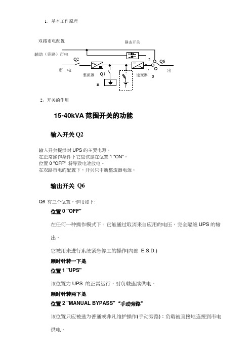
1,基本工作原理双路市电配置静态开关2,开关的作用15-40kVA范围开关的功能输入开关Q2输入开关提供对UPS的主要电源。
在正常操作条件下它应该是在位置1 "ON"。
位置0 "OFF" 将导致电池放电。
在双路市电的配置下,开关只中断整流器电源。
输出开关Q6Q6 有三个位置,作用如下:位置0 "OFF"在任何一种操作模式下,它能通过取消来自应用的电压,完全隔绝UPS的输出。
它被用来进行系统紧急停工的操作(内部 E.S.D.)顺时针转一下是位置1 "UPS"该位置为UPS 的正常运行,对负载连续供电。
顺时针转两下是位置2 "MANUAL BYPASS"“手动旁路”该位置只应被选为普通或非凡维护操作(手动旁路);负载被直接地连接到市电供电。
它可被用于UPS 从辅助市电给应用供电有故障的情形下,在等候技术人员的干预时使用。
电池开关Q13,面板介绍高级模拟面板D2: 表意文字显示区D3: 文本和图形显示区域 BL: 亮光状态条 P1: EXIT 退出 P2: UP 上翻 P3: DOWN 下翻P4: ENTER 回车/OK 确定图标含义BLMASTERYS 3/3 30KVALOAD PROTECTED BATTERY OK P1P2P3P4D3D2亮光条含义光亮条对负载供电的情况提供一个直接的指示显示:红=当前无电源或临近停工。
黄=电源存在但不稳定或临时。
绿=电源安全且稳定。
模拟面板菜单下段描述了模拟面板上可用的菜单以及它们的作用。
如图所示,显示被组织入菜单和子菜单。
访问菜单按ENTER回车键,返回到更高一级菜单,按ESC 。
使用UP 上翻/ DOWN下翻键滚动每级可用的资料信息。
当UPS 被并联连接时,模拟面板显示的系统信息好象这里只有唯一一台UPS 。
选择UPS 数量,显示关于各台机器的信息。
查看报警在正常模式下查看系统报警:从面板操作,按ESC退到原始界面如下:然后按回车键进入SYSTEM按回车进入>ALARM按回车进入>ACTIVE ALARM按回车进入报警详情如:A00:general ALARM。
ELX1147高电流表面装置Brick熔断器技术数据说明书

2822HCHigh current surface mount Brick fuseProduct features• 7.7 x 6.0 x 4.3 mm surface mount package • High current Brick fuse• Current rating: 40 A to 125 A• Voltage rating: Up to 80 Vdc• High interrupting rating• cURus recognized• Single fuse solution for highcurrent applications• Moisture sensitivity level: (MSL): 1Applications• Servers and back planes• Power distribution units (PDUs)• Power supplies• Energy storage system• Industrial automation tools• Robotic machinery• Telecom DC/DC power• Routers & switchesAgency informationcURus Recognition file number: E91958,Guide JFHR2 & JFHR8Environmental complianceHALOGENHFFREE2822HC xx -RTR Family codeAmpere ratingRoHS compliantPackaging codeOrdering part numberPackaging code suffixTR (1000 parts on a 13” diameter tape and reel)2Technical Data ELX1147Effective February 20222822HC High current surface mount Brick fuse/electronicsElectrical characteristicsAmp Rating1.0 Inminimum2.5 Inmaximum40 A ~ 125 A 4 hours 60 secondsProduct specificationsCurrent rating Voltage rating Interrupting rating @ rated voltage 1Typical cold resistance 2Typicalvoltage drop Part number (A)(Vdc)(A)(mΩ)(mV)Part marking2822HC40-R 4072*1000 A @ 72 Vdc 1000 A @ 80 Vdc 1.1075BUSS 2822HC 40A 2822HC50-R 5072*1000 A @ 72 Vdc 1000 A @ 80 Vdc 0.8775BUSS 2822HC 50A 2822HC60-R 6072*1000 A @ 72 Vdc 1000 A @ 80 Vdc 0.78100BUSS 2822HC 60A 2822HC70-R 7072*1000 A @ 72 Vdc 500 A @ 80 Vdc 0.60100BUSS 2822HC 70A 2822HC80-R 8072*1000 A @ 72 Vdc 500 A @ 80 Vdc 0.58100BUSS 2822HC 80A 2822HC90-R 9072*1000 A @ 72 Vdc 500 A @ 80 Vdc 0.54100BUSS 2822HC 90A 2822HC100-R 10072*1000 A @ 72 Vdc 500 A @ 80 Vdc 0.45100BUSS 2822HC 100A 2822HC125-R125601000 A @ 60 Vdc0.40110BUSS 2822HC 125A1. DC Interrupting rating (measured at designated voltage, time constant of less than 1 mlliseconds, battery source)2. Typical cold resistance is measured at <10% of rated current in ambient temperature of +25 °C *= UL rated at 72 Vdc and 80 VdcDimensions- mmDrawing not to scaleAmp ratingL W T W1T140 A - 90 A 7.6 ± 0.30 6.0 ± 0.30 4.2 ± 0.20 5.0 REF 1.6 REF 100 A - 125 A 7.7 ± 0.306.0 ± 0.304.3 ± 0.305.0 REF1.6 REFRecommended pad layoutStandard test boardTesting board: 1.6 mm FR4 PCBCopper thickness: 3 oz for 40 A – 70 A, 6 oz for above 70 A. Tin plated3Technical Data ELX1147Effective February 20222822HCHigh current surface mount Brick fuse /electronicsPackaging information - mm1000 parts per 13” diameter reel (EIA-481 compliant) Drawing not to scaleDimension millimeterW 16.0F 7.5E 1.75P0 4.0P 12.0P2 2.0ØD0 1.50ØD1N/A A0 6.3B08.0K04.7Reel dimension- mmDimensionmillimeterA 330B 2.2C 13.5D 22W116.5W222.4 maximumGeneral specificationsOperating temperature: -40 °C to +125 °C with proper derating factor appliedSoldering heat resistance: MIL-STD-202 method 210, Solder temperature +260 ±5 °C, solder immersion time 10±5 s Solderability test: J-STD-002, method B1, Steam aging 1 hour, Solder temperature + 255 ±5 °C, solder immersion time 5 sThermal shock: MIL-STD-202 method 107, -40 °C/+125 °C. 1000 cycles, maximum transfer time 20 seconds, Dwell time 15 minutes. Air-Air Humidity bias: MIL-STD-202 method 103, 1000 hours +85 °C/85% RH. at 10% of operating power. Vibration: MIL-STD-202F method 201, 2 hours each of 3 orientations. Test from 10-55 Hz for 1 minute Mechanical shock: MIL-STD-202 method 213, Figure 1 of Method 213. Condition C 100 g 6 msHigh temperature operating life: MIL-STD-202 method 108, Condition D steady state TA=+70 °C at 60% rated current.4Technical Data ELX1147Effective February 20222822HC High current surface mount Brick fuse/electronicsT emperature derating curveD e r a t i n g f a c t o rT emperature (°C)I 2t vs. time curveI 2t (A 2s )Time (seconds)Time vs. current curveCurrent (A)T i m e (s e c o n d s )I 2t vs. currentI 2t (A 2s )Current (A)5Technical Data ELX1147Effective February 20222822HCHigh current surface mount Brick fuse /electronics T e m p e r a t u r eTimeT T T T ReferenceProfile featureStandard SnPb solderLead (Pb) free solderPreheat • Temperature min. (T smin )100 °C 100 °C • Temperature typ. (T styp )120 °C 120 °C • Temperature max. (T smax )130 °C 130 °C • Time (T smin to T smax ) (t s )70 seconds 70 seconds D preheat to max Temperature150 °C max.150 °C max.Peak temperature (T P )*235 °C – 260 °C 250 °C – 260 °C Time at peak temperature (t p ) 6 seconds max3 seconds max each wave 6 seconds max3 seconds max each wave Ramp-down rate~ 2 K/s min ~3.5 K/s typ ~5 K/s max ~ 2 K/s min ~3.5 K/s typ ~5 K/s max Time 25 °C to 25 °C4 minutes4 minutesManual solder+350 °C (4-5 seconds by soldering iron), generally manual/hand soldering is not recommended.Wave solder profileEatonElectronics Division 1000 Eaton Boulevard Cleveland, OH 44122United States/electronics© 2022 EatonAll Rights Reserved Printed in USAPublication No. ELX1147 BU-ELX22002February 20222822HC High current surface mount Brick fuseTechnical Data ELX1147Effective February 2022Life Support Policy: Eaton does not authorize the use of any of its products for use in life support devices or systems without the express writtenapproval of an officer of the Company. Life support systems are devices which support or sustain life, and whose failure to perform, when properly used in accordance with instructions for use provided in the labeling, can be reasonably expected to result in significant injury to the user.Eaton reserves the right, without notice, to change design or construction of any products and to discontinue or limit distribution of any products. Eaton also reserves the right to change or update, without notice, any technical information contained in this bulletin.Solder reflow profileT e m p e r a t u r eT LT PEaton is a registered trademark.All other trademarks are property of their respective owners.Follow us on social media to get the latest product and support information.Reference J-STD-020Profile featureStandard SnPb solderLead (Pb) free solderPreheat and soak • Temperature min. (T smin )100 °C 150 °C • Temperature max. (T smax )150 °C 200 °C • Time (T smin to T smax ) (t s )60-120 seconds 60-120 seconds Ramp up rate T L to T p 3 °C/ second max. 3 °C/ second max.Liquidous temperature (T l ) Time (t L ) maintained above T L183 °C60-150 seconds 217 °C60-150 seconds Peak package body temperature (T P )*Table 1Table 2Time (t p )* within 5 °C of the specified classification temperature (T c )20 seconds*30 seconds*Ramp-down rate (T p to T L ) 6 °C/ second max. 6 °C/ second max.Time 25 °C to peak temperature6 minutes max.8 minutes max.* Tolerance for peak profile temperature (T p ) is defined as a supplier minimum and a user maximum.Table 1 - Standard SnPb solder (T c )Package thicknessVolume mm3 <350Volume mm3 ≥350<2.5 mm 235 °C 220 °C ≥2.5 mm220 °C220 °CTable 2 - Lead (Pb) free solder (T c )Package thicknessVolume mm 3 <350Volume mm 3350 - 2000Volume mm 3 >2000<1.6 mm 260 °C 260 °C 260 °C 1.6 – 2.5 mm 260 °C 250 °C 245 °C >2.5 mm250 °C245 °C245 °C。
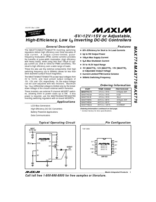
MAX774中文资料
SHDN REF
FB REF GND OUT
MAX774 MAX775 MAX776
7 6 5
DIP/SO
________________________________________________________________ Maxim Integrated Products
1
Call toll free 1-800-998-8800 for free samples or literature.
ELECTRICAL CHARACTERISTICS
PARAMETER V+ Input Voltage Range SYMBOL V+
(V+ = 5V, ILOAD = 0mA, CREF = 0.1µF, TA = TMIN to TMAX, unless otherwise noted. Typical values are at TA = +25°C.) CONDITIONS V+ = 16.5V, SHDN ≤ 0.4V (operating) Supply Current V+ = 10V, SHDN ≥ 1.6V (shutdown) V+ = 16.5V, SHDN ≥ 1.6V (shutdown) FB Trip Point 3V ≤ V+ ≤ 16.5V MAX77_C FB Input Current IFB MAX77_E MAX77_M MAX774 Output Voltage VOUT MAX775 MAX776 MAX77_C Reference Voltage VREF IREF = 0µA MAX77_E MAX77_M REF Load Regulation REF Line Regulation Output Voltage Line Regulation (Circuit of Figure 2— Bootstrapped) Output Voltage Load Regulation (Circuit of Figure 2— Bootstrapped) 0µA ≤ IREF ≤ 100µA 3V ≤ V+ ≤ 16.5V MAX774, 4V ≤ V+ ≤ 15V, ILOAD = 0.5A MAX775, 4V ≤ V+ ≤ 8V, ILOAD = 0.2A MAX776, 4V ≤ V+ ≤ 6V, ILOAD = 0.1A MAX774, 0A ≤ ILOAD ≤ 1A, V+ = 5V MAX775, 0mA ≤ ILOAD ≤ 500mA, V+ = 5V MAX776, 0mA ≤ ILOAD ≤ 400mA, V+ = 5V MAX77_C/E MAX77_M -4.80 -11.52 -14.40 1.4700 1.4625 1.4550 -5 -12 -15 1.5 1.5 1.5 4 4 40 0.035 0.088 0.137 1.5 1.5 1.0 mV/A mV/V -10 2 4 10 ±50 ±70 ±90 -5.20 -12.48 -15.60 1.5300 1.5375 1.5450 10 15 100 mV µV/V V V nA mV MIN 3.0 TYP MAX 16.5 100 5 µA UNITS V
- 1、下载文档前请自行甄别文档内容的完整性,平台不提供额外的编辑、内容补充、找答案等附加服务。
- 2、"仅部分预览"的文档,不可在线预览部分如存在完整性等问题,可反馈申请退款(可完整预览的文档不适用该条件!)。
- 3、如文档侵犯您的权益,请联系客服反馈,我们会尽快为您处理(人工客服工作时间:9:00-18:30)。
MAX1146–MAX1149
The MAX1146–MAX1149 low-power, 14-bit, multichannel, analog-to-digital converters (ADCs) feature an internal track/hold (T/H), voltage reference, and clock. The MAX1146/MAX1148 operate from a single +4.75V to +5.25V supply, and the MAX1147/MAX1149 operate from a single +2.7V to +3.6V supply. All analog inputs are software configurable for unipolar/bipolar and single-ended/differential operation. The 4-wire serial interface connects directly to SPI™/QSPI™/MICROWIRE™ devices without external logic. The serial strobe output (SSTRB) allows convenient connection to digital signal processors. The MAX1146–MAX1149 use an internal clock or an external serial-interface clock to perform successive-approximation analog-to-digital conversions. The MAX1146/MAX1148 include an internal +4.096V reference, while the MAX1147/MAX1149 include an internal +2.500V reference. All devices accept an external reference from 1.5V to VDD. The MAX1146–MAX1149 provide a hardware shutdown and two software power-down modes. Using the software power-down modes allows the devices to be powered down between conversions. When powered down, accessing the serial interface automatically powers up the devices. The quick turn-on time allows power-down between all conversions. This technique reduces supply current to under 120µA for quick turn-on. The MAX1146–MAX1149 are available in a 20-pin TSSOP package.
元器件交易网
Multichannel, True-Differential, Serial, 14-Bit ADCs MAX1146–MAX1149
ABSOLUTE MAXIMUM RATINGS
VDD to AGND, DGND ............................................-0.3V to +6.0V AGND to DGND.....................................................-0.3V to +0.3V CH0–CH7, COM to AGND..........................-0.3V to (VDD + 0.3V) REF, REFADJ to AGND ..............................-0.3V to (VDD + 0.3V) Digital Inputs to DGND...............................-0.3V to (VDD + 0.3V) Digital Outputs to DGND ............................-0.3V to (VDD + 0.3V) Digital Output Sink Current .................................................25mA Continuous Power Dissipation (TA = +70°C) 20 TSSOP (derate 10.9mW/°C above +70°C) .............879mW Operating Temperature Ranges MAX114_ BC_ _ ..................................................0°C to +70°C MAX114_ BE_ _ ...............................................-40°C to +85°C Storage Temperature Range .............................-60°C to +150°C Lead Temperature (soldering, 10s) .................................+300°C
Stresses beyond those listed under “Absolute Maximum Ratings” may cause permanent damage to the device. These are stress ratings only, and functional operation of the device at these or any other conditions beyond those indicated in the operational sections of the specifications is not implied. Exposure to absolute maximum rating conditions for extended periods may affect device reliability.
PARAMETER DC ACCURACY (Note 1) Resolution Relative Accuracy (Note 2) Differential Nonlinearity Offset Error Offset Temperature Coefficient Gain Error Gain Temperature Coefficient Channel-to-Channel Offset Matching Channel-to-Channel Gain Matching (Note 3) ±0.8 ±1 ±1 0.3 ±20 INL DNL No missing codes over temperature -1.0 14 ±0.7 ±0.5 ±2 +1.5 ±10 Bits LSB LSB LSB ppm/°C LSB ppm/°C LSB LSB SYMBOL CONDITIONS MIN TYP MAX UNITS
ELECTRICAL CHARACTERISTICS
(VDD = 5V (MAX1146/MAX1148), VDD = 3.3V (MAX1147/MAX1149), SHDN = VDD, VCOM = 0, fSCLK = 2.1MHz, external clock (50% duty cycle), 18 clocks/conversion (116ksps), VREFADJ = VDD, CREF = 2.2µF, external +4.096V reference at REF (MAX1146/ MAX1148), external 2.500V reference at REF (MAX1147/MAX1149), TA = TMIN to TMAX, unless otherwise noted. Typical values are at TA = +25°C.)
________________________________________________________________ Maxim Integrated Products