BAT54S
常用贴片二极管丝印和参数对应表

常用贴片二极管丝印和参数对应表一、常用贴片二极管丝印和参数对应表在电子元器件中,常用贴片二极管是一种重要的电子元件,具有广泛的应用。
了解二极管的丝印和参数对应关系,对于正确选择和使用二极管具有重要意义。
下面是常用贴片二极管丝印和参数对应表:1. 丝印:1N4148参数:最大反向电压(Vrrm):100V最大反向电流(Ir):150mA正向压降(Vf):1V最大连续工作温度(Tj):200℃2. 丝印:1N4007参数:最大反向电压(Vrrm):1000V最大反向电流(Ir):30mA正向压降(Vf):1V最大连续工作温度(Tj):150℃3. 丝印:1N5819参数:最大反向电压(Vrrm):40V最大反向电流(Ir):1mA正向压降(Vf):0.45V最大连续工作温度(Tj):125℃4. 丝印:BAT54S参数:最大反向电压(Vrrm):30V最大反向电流(Ir):100nA正向压降(Vf):0.32V最大连续工作温度(Tj):150℃5. 丝印:BAV99参数:最大反向电压(Vrrm):85V最大反向电流(Ir):2μA正向压降(Vf):0.8V最大连续工作温度(Tj):150℃二、结语通过以上常用贴片二极管丝印和参数对应表,我们可以清楚地了解到不同型号的贴片二极管的丝印和参数之间的对应关系。
在选择和应用贴片二极管时,我们可以根据需要的电压、电流和温度等参数,选择合适的型号的贴片二极管。
这样能够确保电路的正常工作,提高电子产品的性能和可靠性。
希望以上内容对您了解常用贴片二极管丝印和参数对应关系有所帮助。
如果您对其他电子元器件的丝印和参数对应关系也感兴趣,欢迎提出,我们将为您提供更多相关信息。
BAT54系列PDF资料
DATA SHEETProduct specificationSupersedes data of 2001Oct 122002Mar 04DISCRETE SEMICONDUCTORSBAT54 seriesSchottky barrier (double) diodes ook, halfpageM3D088Schottky barrier (double) diodes BAT54 seriesFEATURES•Low forward voltage•Guard ring protected•Small plastic SMD package.APPLICATIONS•Ultra high-speed switching•Voltage clamping•Protection circuits•Blocking diodes.DESCRIPTIONPlanar Schottky barrier diodes encapsulated in a SOT23 small plastic SMD package. Single diodes and double diodes with different pinning are available.MARKINGNote1.∗=p:Made in Hong Kong.∗=t:Made in Malaysia.∗=W: Made in China.PINNINGTYPE NUMBER MARKING CODE(1) BA T54L4∗BA T54A L42 or∗V3BA T54C L43 or∗W1BA T54S L44 or∗V4PINDESCRIPTIONBAT54BAT54A BAT54C BAT54S 1a k1a1a12n.c.k2a2k23k a1,a2k1,k2k1,a2 handbook, 2 columns213MGC421Top viewFig.1Simplified outline (SOT23) and pinconfiguration.312MLC360312MLC359312MLC358 Fig.2 Diode configuration and symbol.312n.c.MLC357(1)BAT54(2)BAT54A(3)BAT54C(4)BAT54SSchottky barrier (double) diodesBA T54 series LIMITING VALUESIn accordance with the Absolute Maximum Rating System (IEC 60134).THERMAL CHARACTERISTICSNote1.Refer to SOT23 standard mounting conditions.CHARACTERISTICST amb =25°C unless otherwise specified.SYMBOLPARAMETER CONDITIONS MIN.MAX.UNIT Per diodeV Rcontinuous reverse voltage −30V I Fcontinuous forward current −200mA I FRMrepetitive peak forward current t p ≤1s;δ≤0.5−300mA I FSMnon-repetitive peak forward current t p <10ms −600mA T stgstorage temperature −65+150°C T jjunction temperature −125°C Per deviceP tot total power dissipation T amb ≤25°C −230mW SYMBOLPARAMETER CONDITIONS VALUE UNIT R th j-athermal resistance from junction to ambient note 1500K/W SYMBOLPARAMETER CONDITIONS MAX.UNIT Per diodeV F forward voltage see Fig.3I F =0.1mA240mV I F =1mA320mV I F =10mA400mV I F =30mA500mV I F =100mA800mV I Rreverse current V R =25V; see Fig.42µA t rr reverse recovery time when switched from I F =10mAto I R =10mA; R L =100Ω;measured at I R =1mA;see Fig.65ns C d diode capacitance f =1MHz; V R =1V; see Fig.510pFSchottky barrier (double) diodes BA T54 series handbook, halfpage10I FV F (V)310(mA)21011011.20.80.40MSA892(3)(2)(1)(3)(2)(1)(1)T amb =125°C.(2)T amb =85°C.(3)T amb =25°C.Fig.3Forward current as a function of forward voltage; typical values.0102030V (V)R 103I R (µA)102101101(1)(2)(3)MSA893(1)T amb =125°C.(2)T amb =85°C.(3)T amb =25°C.Fig.4Reverse current as a function of reverse voltage; typical values.handbook, halfpage 0102030051015V R (V)C d(pF)MSA891Fig.5Diode capacitance as a function of reversevoltage; typical values.f =1MHz; T amb =25°C.Fig.6 Reverse recovery definitions.handbook, halfpage 90%10%t f Q dI dttI FI R MRC129 - 1FrSchottky barrier (double) diodesBA T54 series PACKAGE OUTLINE UNITA 1max.b p c D E e 1H E L p Q w v REFERENCES OUTLINEVERSIONEUROPEAN PROJECTION ISSUE DATE 97-02-2899-09-13IEC JEDEC EIAJ mm 0.10.480.380.150.09 3.02.8 1.41.20.95e 1.9 2.52.10.550.450.10.2DIMENSIONS (mm are the original dimensions)0.450.15 SOT23TO-236AB b p D e 1e AA 1L p Qdetail X H E E w M v M AB A B 012 mmscale A 1.10.9cX123Plastic surface mounted package; 3 leads SOT23Schottky barrier (double) diodesBA T54 series DATA SHEET STATUSNotes1.Please consult the most recently issued data sheet before initiating or completing a design.2.The product status of the device(s) described in this data sheet may have changed since this data sheet waspublished. The latest information is available on the Internet at URL .DATA SHEET STATUS (1)PRODUCT STATUS (2)DEFINITIONS Objective data Development This data sheet contains data from the objective specification for productdevelopment. Philips Semiconductors reserves the right to change thespecification in any manner without notice.Preliminary data Qualification This data sheet contains data from the preliminary specification.Supplementary data will be published at a later date. PhilipsSemiconductors reserves the right to change the specification withoutnotice, in order to improve the design and supply the best possibleproduct.Product data ProductionThis data sheet contains data from the product specification. PhilipsSemiconductors reserves the right to make changes at any time in orderto improve the design, manufacturing and supply. Changes will becommunicated according to the Customer Product/Process ChangeNotification (CPCN) procedure SNW-SQ-650A.DEFINITIONSShort-form specification The data in a short-formspecification is extracted from a full data sheet with thesame type number and title. For detailed information seethe relevant data sheet or data handbook.Limiting values definition Limiting values given are inaccordance with the Absolute Maximum Rating System(IEC 60134). Stress above one or more of the limitingvalues may cause permanent damage to the device.These are stress ratings only and operation of the deviceat these or at any other conditions above those given in theCharacteristics sections of the specification is not implied.Exposure to limiting values for extended periods mayaffect device reliability.Application information Applications that aredescribed herein for any of these products are forillustrative purposes only. Philips Semiconductors makeno representation or warranty that such applications will besuitable for the specified use without further testing ormodification.DISCLAIMERS Life support applications These products are not designed for use in life support appliances, devices, or systems where malfunction of these products can reasonably be expected to result in personal injury.Philips Semiconductors customers using or selling these products for use in such applications do so at their own risk and agree to fully indemnify Philips Semiconductors for any damages resulting from such application.Right to make changes Philips Semiconductors reserves the right to make changes,without notice,in the products, including circuits, standard cells, and/or software, described or contained herein in order to improve design and/or performance. Philips Semiconductors assumes no responsibility or liability for the use of any of these products,conveys no licence or title under any patent, copyright, or mask work right to these products,and makes no representations or warranties that these products are free from patent, copyright, or mask work right infringement, unless otherwise specified.。
BAT54SDW贴片三极管规格书

A,Sep,2010
A,Sep,2010
【领先的片式无源器整合供应商—南京南山半导体有限公司】
ELECTRICAL CHARACTERISTICS(Ta=25℃ unless otherwise specified)
Parameter Reverse voltage Reverse current Symbol V(BR) IR IR=100μA VR=25V IF=1mA Forward voltage VF IF=10mA IF=30mA IF=100mA Total capacitance Reverse recovery time Ctot trr VR=1V,f=1MHz IF= IR=10mA, Irr=0.1×IR, RL=100Ω Test conditions Min 30 2 320 400 500 1000 10 5 pF ns mV Typ Max Unit V μA
Symbol VRRM VRWM VR IO IFRM IFSM PD RΘJA Tj Tstg Parameter Repetitive Peak Reverse Voltage Peak Working Reverse Voltage DC Blocking Voltage Forward Continuous Current Repetitive Peak Forward Current Non-repetitive Peak Forward Surge Current @t≤1s Power Dissipation Thermal Resistance From Junction To Ambient Junction Temperature Storage Temperature 200 300 600 200 500 125 -55~+150 mA mA mW ℃/W ℃ ℃ 30 V Value Unit
BAT54S BAT54肖特基二极管参数
℃
TJ
Operating Junction Temperature工作结温
-55 to +150
℃
电气特性:
符号
Parameter参数
Conditions测试条件
最小
最大
单位
VR
Breakdown Voltage击穿电压
IR30-Fra bibliotekVVF
Forward Voltage正向电压
IF = 0.1mA
IF = IR = 10mA, IRR = 1.0mA,
RL = 100Ω
-
5.0
nS
BAT54封装外型及引脚图
BAT54
BAT54A
BAT54C
BAT54S
BAT54FILM
BAT54AFILM
BAT54CFILM
BAT54SFILM
BAT54S BAT54肖特基二极管参数
来源:|时间:2010年05月02日
三端贴片肖特基二极管BAT54/BAT54A/BAT54C/BAT54S
特点:
极小传导损耗
开关损耗可以忽略不计
低正向压降
表面贴装器件
肖特基势垒二极管封装采用SOT-23
绝对最大额定值:
Symbol符号
Parameter参数
Value数值
Unit单位
VRRM
Maximum Repetitive Reverse Voltage最大重复反向电压
30
V
IF(AV)
Average Rectified Forward Current平均正向电流整流
200
mA
IFSM
BAT54S-T1中文资料

BAT54 / A / C / SSURFACE MOUNT SCHOTTKY BARRIER DIODECharacteristicSymbol ValueUnitPeak Repetitive Reverse Voltage Working Peak Reverse Voltage DC Blocking Voltage V RRMV RWM V R 30V Average Rectified Output Current I O 100mA Forward Continuous Current (Note 1)I F 200mA Repetitive Peak Forward Current (Note 1)I FRM 300mA Forward Surge Current @ t p <1.0s (Note 1)I FSM 600mA Power Dissipation (Note 1)P d 200mW Typical Thermal Resistance, Junction to Ambient Air R JA 500K/W Operating and Storage Temperature Range T j , T STG-65 to +125°CNote: 1. Device on fiberglass substrate.W T EWER SEMICONDUCTORSMaximum Ratings and Electrical Characteristics, Single Diode@TA=25°C unless otherwise specified Characteristic Symbol Min Typ Max Unit Test ConditionReverse Breakdown Voltage V(BR)R30——V I RS = 100µAForward Voltage V F——2403204005001000mVtp <300µs, duty cycle <2%@I F = 0.1mA@I F = 1mA@I F = 10mA@I F = 30mA@I F = 100mAReverse Leakage Current I R—— 2.0µAtp < 300µs, duty cycle <2% @ V R = 25VJunction Capacitance C j——10pF V R = 1.0V, f = 1.0MHzReverse Recovery Time t rr—— 5.0nSI F = 10mA through I R = 10mA to I R = 1.0mA, R L = 100ORDERING INFORMATIONProduct No.!Package TypeShipping QuantityBAT54-T1SOT-233000/Tape & Reel BAT54-T3SOT-2310000/Tape & Reel BAT54A-T1SOT-233000/Tape & Reel BAT54A-T3SOT-2310000/Tape & Reel BAT54C-T1SOT-233000/Tape & Reel BAT54C-T3SOT-2310000/Tape & Reel BAT54S-T1SOT-233000/Tape & Reel BAT54S-T3SOT-2310000/Tape &ReelProducts listed in bold are WTE Preferred devices.!T1 suffix refers to a 7” reel. T3 suffix refers to a 13” reel.Shipping quantity given is for minimum packing quantity only. For minimum order quantity, please consult the Sales Department.RECOMMENDED FOOTPRINTWon-Top Electronics Co., Ltd (WTE) has checked all information carefully and believes it to be correct and accurate. However, WTE cannot assume any responsibility for inaccuracies. Furthermore, this information does not give the purchaser of semiconductor devices any license under patent rights to manufacturer. WTE reserves the right to change any or all information herein without further notice.WARNING : DO NOT USE IN LIFE SUPPORT EQUIPMENT. WTE power semiconductor products are not authorized for use as critical components in life support devices or systems without the express written approval.We power your everyday.Won-Top Electronics Co., Ltd.No. 44 Yu Kang North 3rd Road, Chine Chen Dist., Kaohsiung, Taiwan Phone: 886-7-822-5408 or 886-7-822-5410Fax: 886-7-822-5417Email: sales@Internet: 。
BAT54SLT1G双向肖特基二极管规格书

Dual Series Schottky Barrier Diodes
BAT54SLT1G
These Schottky barrier diodes are designed for high speed switching applications, circuit protection, and voltage clamping. Extremely low forward voltage reduces conduction loss. Miniature surface mount package is excellent for hand held and portable applications where space is limited.
Characteristic
Symbol
Min
Typ
Reverse Breakdown Voltage (IR = 10 µA) Total Capacitance (VR = 1.0 V, f = 1.0 MHz) Reverse Leakage (VR = 25 V)
V(BR)R
30
—
CT
—
—
IR
@ TA = 25°C
PD
Derate above 25°C
Forward Current (DC)
IF
Junction Temperature
TJ
Storage Temperature Range
Tstg
Value 30
225 1.8 200 Max 125 Max – 55 to +150
ELECTRICAL CHARACTERISTICS (TA = 25°C unless otherwise noted) (EACH DIODE)
BAT54S 保护电路
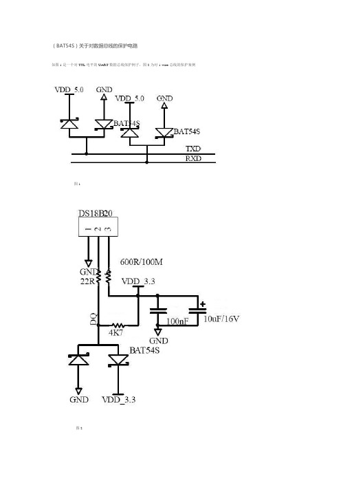
(BAT54S)关于对数据总线的保护电路如图1是一个对TTL电平的UART数据总线保护例子,图2为对1-wire总线的保护案例图1图2BAT54S是肖特基二极管,肖特基二极管是以其发明人肖特基博士(Schottky)命名的,SBD是肖特基势垒二极管(SchottkyBarrierDiode,缩写成SBD)的简称。
SBD不是利用P型半导体与N型半导体接触形成PN结原理制作的,而是利用金属与半导体接触形成的金属-半导体结原理制作的。
因此,SBD也称为金属-半导体(接触)二极管或表面势垒二极管,它是一种热载流子二极管。
优缺点是近年来问世的低功耗、大电流、超高速半导体器件。
其反向恢复时间极短(可以小到几纳秒),正向导通压降仅0.4V左右,而整流电流却可达到几千毫安。
这些优良特性是快恢复二极管所无法比拟的。
中、小功率肖特基整流二极管大多采用封装形式。
SBD具有开关频率高和正向压降低等优点,但其反向击穿电压比较低,大多不高于60V,最高仅约100V,以致于限制了其应用范围。
像在开关电源(SMPS)和功率因数校正(PFC)电路中功率开关器件的续流二极管、变压器次级用100V以上的高频整流二极管、RCD缓冲器电路中用600V~1.2kV的高速二极管以及PFC升压用600V二极管等,只有使用快速恢复外延二极管(FRED)和超快速恢复二极管(UFRD)。
目前UFRD的反向恢复时间Trr也在20ns以上,根本不能满足像空间站等领域用1MHz~3MHz的SMPS需要。
即使是硬开关为100kHz的SMPS,由于UFRD的导通损耗和开关损耗均较大,壳温很高,需用较大的散热器,从而使SMPS体积和重量增加,不符合小型化和轻薄化的发展趋势。
因此,发展100V 以上的高压SBD,一直是人们研究的课题和关注的热点。
近几年,SBD已取得了突破性的进展,150V和200V的高压SBD已经上市,使用新型材料制作的超过1kV的SBD也研制成功,从而为其应用注入了新的生机与活力。
常用二极管型号及参数大全
常用二极管型号及参数大全
二极管是一种最常用的电子器件之一,它具有方便、可靠、低成本等优点,在电子领域被广泛应用。
常用的二极管型号和参数有很多,下面我将介绍一些常见的二极管型号及其参数。
1.PN结二极管:
型号:1N4148
参数:正向电压降:0.7V,反向最大电压:75V,最大连续电流:
300mA
2.快恢复二极管:
型号:1N4937
参数:正向电压降:1.2V,反向最大电压:600V,最大连续电流:1A 3.高速二极管:
型号:BAT54
参数:正向电压降:0.55V,反向最大电压:30V,最大连续电流:350mA
4.整流二极管:
型号:1N4007
参数:正向电压降:1V,反向最大电压:1000V,最大连续电流:1A 5.功率二极管:
型号:1N5408
参数:正向电压降:1.2V,反向最大电压:1000V,最大连续电流:3A 6.双向导通二极管:
型号:BAT54S
参数:正向电压降:0.55V,反向最大电压:30V,最大连续电流:650mA
7. Zenner二极管:
型号:1N4742A
参数:正向电压降:1.2V,反向最大电压:12V,最大电流:1W
8.稳压二极管:
型号:1N5231B
参数:正向电压降:0.7V,反向最大电压:4.7V,最大连续电流:0.5W
9.光电耦合二极管:
型号:PC817
参数:正向电压降:1.2V,反向最大电压:80V,最大连续电流:50mA 10.电容二极管:
型号:BB001
参数:正向电压降:1.2V,反向最大电压:6V,最大连续电流:50mA。
- 1、下载文档前请自行甄别文档内容的完整性,平台不提供额外的编辑、内容补充、找答案等附加服务。
- 2、"仅部分预览"的文档,不可在线预览部分如存在完整性等问题,可反馈申请退款(可完整预览的文档不适用该条件!)。
- 3、如文档侵犯您的权益,请联系客服反馈,我们会尽快为您处理(人工客服工作时间:9:00-18:30)。
Small Signal Schottky (double) diodesBAT54N3/BAT54AN3 BAT54CN3/BAT54SN3DescriptionPlanar silicon Schottky barrier diodes encapsulated in a SOT-23 small plastic SMD package. Single diodes and double diodes with different pinning are available.Features•Very small conduction losses •Low forward voltage drop •Small plastic SMD packageApplications•Ultra high-speed switching •V oltage clamping •Protection circuits •Blocking diodesPinning OutlineDescriptionPinBAT54 BAT54A BAT54C BAT54S 1 A K1 A1 A1 2 NC K2 A2 K2 3 K A1,A2 K1,K2 K1,A1 231N.C.123123321SOT-23 123(1) BAT54(3)BAT54C (2)BAT54A(4)BAT54SDiode configuration and symbolMarking:Type Marking Code BAT54 N3 L4BAT54AN3 L42 BAT54CN3 L43 BAT54SN3 L44Absolute Maximum Ratings• Maximum TemperaturesStorage Temperature Tstg................................................................................................... -65~+150 °C Junction Temperature Tj.............................................................................................................. +125°C • Maximum Power DissipationTotal Power Dissipation (Ta=25°C) Ptot (Note)......................................................................... 230 mW • Maximum V oltages and Currents (Ta=25°C)Repetitive Peak Reverse V oltage V RRM .............................................................................................. 30 V Continuous Forward Current I F ................................................................................................... 200 mA Repetitive Peak Forward Current(tp ≤1s,duty cycle ≤0.5)………………………………………… 300mA Non-repetitive Peak Forward Current (tp<10ms, sinusoidal) IFSM ............................................... 600 mA Note:for double diodes, Ptot is the total power dissipation of both diodes. Characteristics (Ta=25°C)Characteristic Symbol Condition Min. Max. UnitReverse Breakdown V oltageV BRI R =100µA 30 - VV F (1) I F =0.1mA - 240 mVV F (2) I F =1mA - 320 mVV F (3) I F =10mA - 400 mVV F (4) I F =30mA - 500 mVForward V oltage (Note 1)V F (5) I F =100mA - 800 mVReverse Leakage Current (Note 2) I R V R =25V ,Tj=25℃ - 2 µA Diode Capacitance C D V R =1V , f=1MHz-10pFReverse Recovery TimetrrI F =I R =10mA R L =100Ω measured at I R =1mA- 5 nsNotes : 1.pulse test, tp=380µs,duty cycle<2%.2.pulse test, tp=5ms,duty cycle<2%.Characteristic CurvesForward Current & Forward Voltage501001502002502004006008001000Forward Voltage-V F (mV)F o r w a r d C u r r e n t -I F (m A )Diode Capacitance & Reverse-Biased Voltage1101000.1110100Reverse Biased Voltage-V R (V)D i o d e C a p a c i t a n c e -C d (p F )SOT-23 Dimension• BAT54AN3: Common Anode. (Marking Code L42) • BAT54CN3: Common Cathode. (Marking Code L43) • BAT54SN3: Series Connected. (Marking Code L44)*: TypicalInches Millimeters Inches MillimetersDIMMin. Max. Min. Max. DIMMin. Max. Min. Max.A 0.1102 0.1204 2.80 3.04 J 0.0034 0.0070 0.85 0.177B 0.0472 0.0630 1.20 1.60 K 0.0128 0.0266 0.32 0.67C 0.0335 0.0512 0.89 1.30 L 0.0335 0.0453 0.85 1.15D 0.0118 0.0197 0.30 0.50 S 0.0830 0.1083 2.10 2.75 G 0.0669 0.0910 1.70 2.30 V 0.0098 0.0256 0.25 0.65 H 0.0005 0.0040 0.013 0.10Notes: 1.Controlling dimension: millimeters. 2.Maximum lead thickness includes lead finish thickness, and minimum lead thickness is the minimum thickness of base material.3.If there is any question with packing specification or packing method, please contact your local CYStek sales office.Material:• Lead: 42 Alloy; solder plating• Mold Compound: Epoxy resin family, flammability solid burning class: UL94V-0Important Notice:• All rights are reserved. Reproduction in whole or in part is prohibited without the prior written approval of CYStek. • CYStek reserves the right to make changes to its products without notice.• CYStek semiconductor products are not warranted to be suitable for use in Life-Support Applications, or systems.• CYStek assumes no liability for any consequence of customer product design, infringement of patents, or application assistance.HJKDAL GV CB321SMarking:L4_Diagram:3-Lead SOT-23 Plastic Surface MountedPackage. CYStek Package Code: N3L4XThis datasheet has been downloaded from:Free DownloadDaily Updated Database100% Free Datasheet Search Site100% Free IC Replacement Search SiteConvenient Electronic DictionaryFast Search SystemAll Datasheets Cannot Be Modified Without PermissionCopyright © Each Manufacturing Company。