LINEAR LTC6804-1
基于LTC6804的电池参数采集系统设计
基于LTC6804的电池参数采集系统设计
摘要:分析目前电池参数采集的方法,提出采用LTC6804 进行电池参数采集的方法。
电池参数采集系统硬件包括LTC6804 单体电池电压检测、NTC 温度检测、LT3990 供电、dsPIC30F 控制部分、通信隔离等。
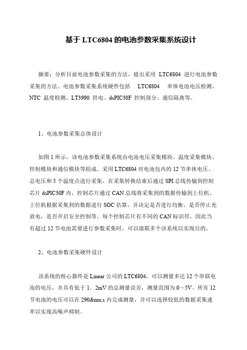
1、电池参数采集总体设计
如图1所示,该电池参数采集系统由电池电压采集模块、温度采集模块、控制模块和通信模块等组成。
采用LTC6804对电池包内的12节单体电压、总电压和5个温度点进行采集,在采集转换结束后通过SPI总线传输到控制芯片dsPIC30F内,控制芯片通过CAN总线将采集到的数据传输到上位机。
上位机根据采集到的数据进行SOC估算,并决定是否进行均衡,是否停止充放电,是否开启安全控制等。
每个控制芯片有不同的CAN标识符,因此当有超过12节电池需要进行参数采集时,可以级联多个该系统以实现目的。
2、电池参数采集硬件设计
该系统的核心器件是Linear公司的LTC6804,可以测量多达12个串联电池的电压,并具有低于1.2mV的总测量误差,测量范围为0~5V。
所有12节电池的电压可以在290μs内完成测量,并可以选择较低的数据采集速率以实现高噪声抑制。
具有36V、18V和Type_C三种电压输出的锂电池组的生产技术

本技术新型涉及一种具有36V、18V和Type_C三种电压输出的锂电池组。
包括串联连接的10节锂离子单体电池、带有通信接口的电池参数检测电路、带有通信接口的单片机、第一至第二场效应管驱动电路、第一至第四场效应管、第一至第二熔断器、双向DC/DC转换电路、Type C接口。
本技术新型使电池组的功能得到扩展,并且电源的转换效率很高,使电池组可以有多种输出电压,能应用于多类消费类电子产品进行供电,包括电动助力车、笔记本电脑、手机、路由器等等。
技术要求1.一种具有36V、18V和Type_C三种电压输出的锂电池组,其特征在于,包括串联连接的10节锂离子单体电池、带有通信接口的电池参数检测电路、带有通信接口的单片机、第一至第二场效应管驱动电路、第一至第四场效应管、双向DC/DC转换电路、Type-C接口;串联连接的10节锂离子单体电池的每个节点均与电池参数检测电路连接,第一节锂离子单体电池的负极与第四场效应管的S 极连接,第四场效应管的D极与第三场效应管的S极、双向DC/DC转换电路的输入负极连接,并作为整个锂电池组的输出负极,第十节锂电子单体电池的正极与第一场效应管的D极连接,第一场效应管的S极与第二场效应管的D极、双向DC/DC转换电路的输入正极连接,并作为整个锂电池组的输出正极,第五节锂离子单体电池与第六节锂离子单体电池的连接节点与第二场效应管的S极、第三场效应管的D极连接,单片机与电池参数检测电路、第一场效应管驱动电路、第二场效应管驱动电路连接,第一场效应管驱动电路与第一场效应管的G极、第二场效应管的G极连接,第二场效应管驱动电路与第三场效应管的G极、第四场效应管的G极连接,双向DC/DC转换电路的输出正负极分别与Type-C接口的正负极连接。
2.根据权利要求1所述的一种具有36V、18V和Type_C三种电压输出的锂电池组,其特征在于,还包括一用于选择输出电压且与单片机连接的开关。
3.根据权利要求1所述的一种具有36V、18V和Type_C三种电压输出的锂电池组,其特征在于,还包括一设于双向DC/DC转换电路的输入正极与整个锂电池组的输出正极之间的电感。
linearltc压电能量收集电源方案
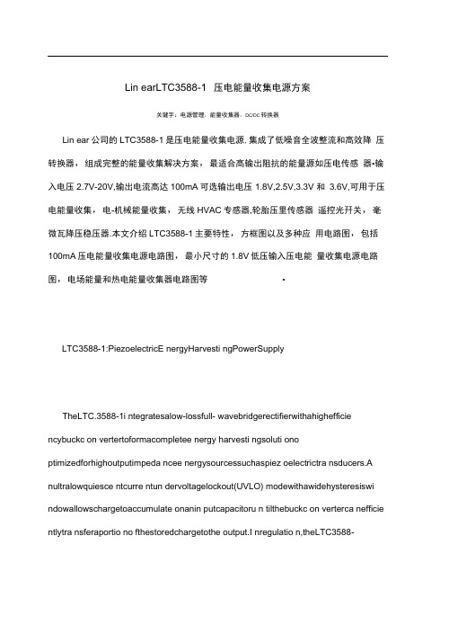
Lin earLTC3588-1 压电能量收集电源方案关键字:电源管理,能量收集器,DC/DC转换器Lin ear公司的LTC3588-1是压电能量收集电源,集成了低噪音全波整流和高效降压转换器,组成完整的能量收集解决方案,最适合高输出阻抗的能量源如压电传感器•输入电压2.7V-20V,输出电流高达100mA可选输出电压1.8V,2.5V,3.3V 和 3.6V,可用于压电能量收集,电-机械能量收集,无线HVAC专感器,轮胎压里传感器遥控光幵关,毫微瓦降压稳压器.本文介绍LTC3588-1主要特性,方框图以及多种应用电路图,包括100mA压电能量收集电源电路图,最小尺寸的1.8V低压输入压电能量收集电源电路图,电场能量和热电能量收集器电路图等•LTC3588-1:PiezoelectricE nergyHarvesti ngPowerSupplyTheLTC.3588-1i ntegratesalow-lossfull- wavebridgerectifierwithahighefficie ncybuckc on vertertoformacompletee nergy harvesti ngsoluti ono ptimizedforhighoutputimpeda ncee nergysourcessuchaspiez oelectrictra nsducers.A nultralowquiesce ntcurre ntun dervoltagelockout(UVLO) modewithawidehysteresiswi ndowallowschargetoaccumulate onanin putcapacitoru n tilthebuckc on verterca nefficie ntlytra nsferaportio no fthestoredchargetothe output.I nregulatio n,theLTC3588-1en tersasleepstate in whichboth in puta ndoutputquiesce ntcurre ntsare mini mal.T hebuckc on vertertur nsonan doffas neededtoma intain regulati on.Fouroutputvoltages,1.8V,2.5V,3.3Va nd3.6V,arepi nselectablewithupto100m Aofcontinu ousoutputcurre nt;however,theoutputcapacitormaybesizedtoservice ahigheroutputcurre ntburst.A nin putprotectivesh un tsetat20Ve nablesgreatere n ergystorageforagive namoun tofi nputcapacita nee.LTC3588-1主要特性:—NoLoad) 950nAln putQuiesce ntCurre nt(Outputi nRegulatio n450nAI nputQuiesce ntCurre nti nUVLO2.7Vto20VI nputOperati ngRa ngeIn tegratedLow-LossFull-WaveBridgeRectifierUptolOOmAofOutputCurre nt SelectableOutputVoltagesof1.8V,2.5V,3.3V,3.6VHighEfficie ncyl ntegratedHystereticBuckDC/DCIn putProtectiveShu nt —Upto25mAPull-Do wn atVIN> 20V WideI nputU ndervoltageLockout(UVLO)Ra ngeAvailablei n10-LeadMSEa nd3mmx3mmDFNPackagesLTC3588-1 应用:PiezoelectricE nergyHarvesti ngElectro-Mecha nicalE nergyHarvesti ngWirelessHVACSe nsors MobileAssetTracki ngTirePressureSe nsors BatteryReplaceme ntforl ndustrialSe nsors RemoteLightSwitchesStan dal on eNa nopowerBuckRegulator著一m函1.LTC3588匕8斎函」sm ApieicE一鱼S-rrl n E a yHaw邕?壬『OCT函 2.L T C3588—l 00m A te [>^K *t >[>M函i图3.LTC3588-13.3V 压电能量收集电源电路图:给带无线发送器的微处理器和 50mA 瞬态负载供电.P 旧电 SYSTEMS T220-.M*^3X_IDI —图4.最小尺寸的1.8V 低压输入压电能量收集电源电路图'h {OPTIONAL}VlH PGCXJDV||Q LTCK3B-1CAPsw D3 VoufDO1O|1FprePGOOOLTC3588-1$w^bur、蟻bl 1帕&0PIEZO STS T230-A4-M3XTtzu=1=T1-q —刖M|lF &vPflPZ? KWCW*|hUC358B-1.B . ¥IIE ■aiiiDI&3GND—■ JU -10UHI J-111FT2Li 卯—r- ?5V I -------1±图5.采用单个压电晶体和自动加电次序的双电源电路图iMU 比4优罚TWIflUHVOUTipF 6V—r^Ev1O0^亠*髦"F "T BYr1OyF25V I ----------------47|f图6.带备份电池的压电能量收集器电路图图7.AC 火线供电的3.6V 降压稳压器,大输出电容支持重负载PANELS ARE PLACED G bFROM T x4' FLUQRfSCFFJT LiflHT FIXTURESGOPPtR 用MEL(情綁刊IDANGER! HIGH VOLTAGE'COPPER PA 忡EL(12* x 24f \—F*GOODPGOQD9V ' BAntHVP1E2O SVSTEMS T2SOW-503XP21p 竝VlHPGOODITG33A8-1CAP SWV|W2Van00P22GHDPGOODPZ2PGOODlTCJ5B8-tswV,-,-vgyr□ lDO RND5p7?v-iPGOODLTO5^0-1GAP5W%V QUTBlI (X JHJ —*1O^F "T" SV图8.电场能量收集器电路图St _L5VT0 f6V•…SOUR PANfL rao5M4X&FrrIPF■VvVT BATTERYII%PiJOODLTG3W1GAP SWy IV3V CVT0001GNDiPG3OD5* 2.7V 蚀FX5V NESS SUPER W^ACITOR_ £5HSR-ODa30O^M2fl7图9.5-16V太阳能供电的2.5V电源,其超大电容增加输出能量存储和备份电池IPG-1 THERMALI GEMERATORMi 61-1,0-127-1.27I (TELLUflEX)—5,4VH工工工[---------1P22%卩GOODUC3506-1CAP畑V OUTDO01GUO跡47pF2.5V图10.热电能量收集器电路图。
LinearLTC3588~1压电能量收集电源方案
Lin ear LTC3588-1压电能量收集电源方案关键字:电源管理,能量收集器,DC/DC转换器Linear公司的LTC3588-1是压电能量收集电源,集成了低噪音全波整流和高效降压转换器,组成完整的能量收集解决方案,最适合高输岀阻抗的能量源如压电传感器•输入电压2.7V-20V,输岀电流高达100mA,可选输出电压1.8V, 2.5V, 3.3V和3.6V,可用于压电能量收集,电-机械能量收集无线HVAC传感器,轮胎压里传感器,遥控光开关,毫微瓦降压稳压器.本文介绍LTC3588-1主要特性,方框图以及多种应用电路图,包括100mA压电能量收集电源电路图,最小尺寸的1.8V低压输入压电能量收集电源电路图,电场能量和热电能量收集器电路图等.LTC3588-1: Piezoelectric Energy Harvesting Power SupplyThe LTC.3588-1 integrates a low-loss full-wave bridge rectifier with a high efficiency buck converter to form a complete energy harvesting solution optimized for high output impedance energy sources such as piezoelectric transducers. An ultralow quiescent current undervoltage lockout (UVLO) mode with a wide hysteresis window allows charge to accumulate on an input capacitor until the buck converter can effi ciently transfer a portion of the stored charge to the output. In regulation, the LTC3588-1 enters a sleep state in which both input and output quiescent currents are minimal. The buck converter turns on and off as needed to maintain regulation.Four output voltages, 1.8V, 2.5V, 3.3V and 3.6V, are pin selectable with up to 100mA of continuous output current; however, the output capacitor may be sized to service a higher output current burst. An input protective shunt set at 20V enables greater energy storage for a given amount of input capacitance.LTC3588-1主要特性:950nA Input Quiescent Current (Output in Regulation - No Load)450nA Input Quiescent Current in UVLO2.7V to 20V Input Operating RangeIntegrated Low-Loss Full-Wave Bridge RectifierUp to 100mA of Output CurrentSelectable Output Voltages of 1.8V, 2.5V, 3.3V, 3.6VHigh Efficiency Integrated Hysteretic Buck DC/DCInput Protective Shunt - Up to 25mA Pull- Down at VIN > 20V Wide Input Undervoltage Lockout (UVLO) RangeAvailable in 10-Lead MSE and 3mm x3mm DFN Packages LTC3588-1 应用:Piezoelectric Energy HarvestingElectro-Mechanical Energy HarvestingWireless HVAC SensorsMobile Asset TrackingTire Pressure SensorsBattery Replacement for Industrial SensorsRemote Light SwitchesStandalone Nanopower Buck Regulator6恤10, 血IIHErUIAl FUILE 31 01 M)L} "T —6V图2.LTC3588-1 100mA 压电能量收集电源电路图图1.LTC3588-1方框图 100mA Piezoelectric Energy Harvesting Power Su 叩ly ACVAWCEO CERAMETPICS PFC-WU BUCK :CCNrROLCSIORAGE25Y rIQpH---- -------------------- 畑 TI 丄< 砒 _H 刖nMi■ ] OUTPUT - ~ VOLTAGESELECTPGOOi?PGOODGWFRFJGR0ALD&APREFERENCE PZ1 PZ2v,Nsw n«&se -i如CAPPGOOO VlPiz00. Q1GRID工图 3.LTC3588-1 3.3V 压电能量收集电源电路图:给带无线发送器的微处理器和50mA 瞬态负载供电.图5.采用单个压电晶体和自动加电次序的双电源电路图PZ1VinmPGOODCAPLTG35W-1 鬧畑hiv tMHU ID9GMDCO^EENhMICROPROCESSORL.・ OpF I --------------------- ' 丄斗卉4 uS图4.最小尺寸的1.8V 低压输入压电能量收集电源电路图眺JO £*STLUSPZ2PZI PGODDDO10pF25V pdOO 序一1—MF "Rev rLTCJsea-iCAP SW图8.电场能量收集器电路图图6•带备份电池的压电能量收集器电路图图7.AC 火线供电的3.6V 降压稳压器,大输出电容支持重负载円㈣:”DANGER HIGH VOLTAGE 1150k信 DkI------------- z\l20VAC创用 1 5Qk 15CH<-T-弭9VBAHEHVPILZO SVSTEMS T22O-W-5WXtR05H40C&?7^rtFPANELS ARE PLACED G bFROM ?' x4' FLUORfSCEM LIGHT FiZTUFtESCCPPfR PAF1ELCOPPER 朋毗LP22V|kjPGOODITC358 &>1CftpSW V|H2VtMJT口DOGHCIF'A QOCP71 P7? V.|PGOODLTC3&B0-13Wv12 VOUTtnGMDPGOOD±±GU二询s图10.热电能量收集器电路图图9.5-16V 太阳能供电的2.5V 电源,其超大电容增加输出能量存储和备份电池10012I Pfi-1 THERMAL |鉅碰RATOR fflie 1-1,0-127-157I llfLLJflEKi丁阳 •ipf ■仙mi -w>5V TO 16VSOLAR PAN5LSVRAnERY[R06H4X5FTRM : HE255 S' PER TAPACiTOR TAW :RF1-'00300-^237—^— i OpfPGO QDP12WinPG&ODLTC358 时CAPBVJ恤0001 GND—團 - |'"4.7|jF 工PZ1PZ2 wPG-OTDLTG35S8-1CAPSW 畑VOUT :DOD1GNDPGOOO。
LTC6401IUD-26#PBF中文资料

1640126fFREQUENCY (MHz)O U T P U T I P3 (d B m )10203040506050100150200640126 TA01bTYPICAL APPLICATIONFEATURESAPPLICATIONSDESCRIPTIONLow Distortion Differential ADC Driver for DC-140MHzThe LTC ®6401-26 is a high-speed differential amplifi er targeted at processing signals from DC to 140MHz. The part has been specifi cally designed to drive 12-, 14- and 16-bit ADCs with low noise and low distortion, but can also be used as a general-purpose broadband gain block.The LTC6401-26 is easy to use, with minimal support circuitry required. The output common mode voltage is set using an external pin, independent of the inputs, which eliminates the need of transformers or AC-coupling ca-pacitors in many applications. The gain is internally fi xed at 26dB (20V/V).The LTC6401-26 saves space and power compared to alternative solutions using IF gain blocks and transform-ers. The LTC6401-26 is packaged in a compact 16-lead 3mm × 3mm QFN package and operates over the –40°C to 85°C temperature range.Equivalent OIP3 vs Frequency■1.6GHz –3dB Bandwidth ■ Fixed Gain of 20V/V (26dB)■ –85dBc IMD3 at 70MHz (Equivalent OIP3 = 46.5dBm)■ –72dBc IMD3 at 140MHz (Equivalent OIP3 = 40dBm)■ 1nV/√H z Internal Op Amp Noise■ 1.5nV/√H z Total Input Referred Noise ■ 6.8dB Noise Figure■ Differential Inputs and Outputs ■ 50Ω Input Impedance■ 2.85V to 3.5V Supply Voltage ■ 45mA Supply Current (135mW)■ 1V to 1.6V Output Common Mode, Adjustable ■ DC- or AC-Coupled Operation■Max Differential Output Swing 4.7V P-P■ Small 16-Lead 3mm × 3mm × 0.75mm QFN Package■Differential ADC Driver ■ Differential Driver/Receiver■ Single Ended to Differential Conversion ■ IF Sampling Receivers ■ SAW Filter InterfacingSingle-Ended to Differential ADC Driver at 140MHz IF0.1μV2640126fABSOLUTE MAXIMUM RATINGSSupply Voltage (V + – V –) ..........................................3.6V Input Current (Note 2) ..........................................±10mA Operating Temperature Range(Note 3) ...............................................–40°C to 85°C Specifi ed Temperature Range(Note 4) ...............................................–40°C to 85°C Storage Temperature Range ...................–65°C to 150°C Maximum Junction Temperature ..........................150°C(Note 1)161514135678TOP VIEW UD PACKAGE16-LEAD (3mm × 3mm) PLA S TIC QFN 9101117124321V +V OCM V +V –V –ENABLE V +V ––I N–I N+I N +I N–O U T–O U T F+O U T F+O U TT JMAX = 150°C, θJA = 68°C/W, θJC = 4.2°C/WEXPOSED PAD (PIN 17) IS V –, MUST BE SOLDERED TO PCBORDER INFORMATIONLEAD FREE FINISH TAPE AND REELPART MARKING*PACKAGE DESCRIPTIONSPECIFIED TEMPERATURE RANGE LTC6401CUD-26#PBF LTC6401CUD-26#TRPBF LCDG 16-Lead (3mm × 3mm) Plastic QFN 0°C to 70°C LTC6401IUD-26#PBFLTC6401IUD-26#TRPBF LCDG16-Lead (3mm × 3mm) Plastic QFN–40°C to 85°CConsult LTC Marketing for parts specifi ed with wider operating temperature ranges. *The temperature grade is identifi ed by a label on the shipping container.Consult LTC Marketing for information on non-standard lead based fi nish parts.For more information on lead free part marking, go to: /leadfree/ For more information on tape and reel specifi cations, go to: /tapeandreel/LTC6400 AND LTC6401 SELECTOR GUIDEPART NUMBER GAIN(dB)GAIN (V/V)Z IN (DIFFERENTIAL)(Ω)I CC (mA)LTC6401-88 2.540045LTC6401-20201020050LTC6401-2626205045LTC6400-20201020090LTC6400-2626205085In addition to the LTC6401 family of amplifi ers, a lower distortion LTC6400 family is available. The LTC6400 is pin compatible to the LTC6401, and has the same low noise performance. The low distortion of the LTC6400 comes at the expense of higher power consumption. Please refer to the separate LTC6400 data sheets for complete details. Other gain versions from 8dB to 14dB will follow.Please check each datasheet for complete details.PIN CONFIGURATIONDC ELECTRICAL CHARACTERISTICSSYMBOL PARAMETER CONDITIONS MIN TYP MAX UNITS Input/Output Characteristic (+IN, –IN, +OUT, –OUT, +OUTF, –OUTF)G DIFF Gain V IN = ±50mV Differential●252627dB TC GAIN Gain Temperature Drift V IN = ±50mV Differential●0.003dB/°C V SWINGMIN Output Swing Low Each Output, V IN = ±200mV Differential●0.090.15V V SWINGMAX Output Swing High Each Output, V IN = ±200mV Differential● 2.3 2.43V V OUTDIFFMAX Maximum Differential Output Swing1dB Compressed● 4.3 4.7V P-P I OUT Output Current Drive Each Output, V IN = ±200mV,V OUT > 2V P-P●10mA V OS Input Offset Voltage Differential●–2.5 2.5mV TCV OS Input Offset Voltage Drift Differential●1μV/°C I VRMIN Input Common Mode Voltage Range, MIN1V I VRMAX Input Common Mode Voltage Range, MAX 1.6V R INDIFF Input Resistance (+IN, –IN)Differential●42.55057.5ΩC INDIFF Input Capacitance (+IN, –IN)Differential, Includes Parasitic1pF R OUTDIFF Output Resistance (+OUT, –OUT)Differential●182532ΩR OUTFDIFF Filtered Output Resistance (+OUTF, –OUTF)Differential●85100115ΩC OUTFDIFF Filtered Output Capacitance (+OUTF, –OUTF)Differential, Includes Parasitic 2.7pF CMRR Common Mode Rejection Ratio Input Common Mode Voltage1.1V to1.4V●5075dB Output Common Mode ControlG CM Common Mode Gain V OCM = 1V to 1.6V1V/VV OCMMIN Output Common Mode Range, MIN●11.1VVV OCMMAX Output Common Mode Range, MAX●1.61.5VVV OSCM Common Mode Offset Voltage V OCM = 1.1V to 1.5V●–1515mV TCV OSCM Common Mode Offset Voltage Drift●3μV/°C IV OCM V OCM Input Current●515μA E N A B L E PinV IL E N A B L E Input Low Voltage●0.8V V IH E N A B L E Input High Voltage● 2.4V I IL E N A B L E Input Low Current E N A B L E = 0.8V●0.5μA I IH E N A B L E Input High Current E N A B L E = 2.4V● 1.43μA Power SupplyV S Operating Supply Range● 2.853 3.5V I S Supply Current E N A B L E = 0V, Both Inputs andOutputs Floating●354560mAI SHDN Shutdown Supply Current E N A B L E = 3V, Both Inputs andOutputs Floating●0.83mAPSRR Power Supply Rejection Ratio (DifferentialOutputs)2.85V to 3.5V●6095.5dBThe● denotes the specifi cations which apply over the full operating temperature range, otherwise specifi cations are at T A = 25°C. V+ = 3V, V– = 0V, +IN = –IN = V OCM = 1.25V, E N A B L E = 0V, No R L unless otherwise noted.3640126fAC ELECTRICAL CHARACTERISTICS Specifi cations are at TA = 25°C. V+ = 3V, V– = 0V, V OCM = 1.25V,E N A B L E = 0V, No R L unless otherwise noted.SYMBOL PARAMETER CONDITIONS MIN TYP MAX UNITS –3dBBW–3dB Bandwidth200mV P-P,OUT (Note 6) 1.2 1.6GHz 0.5dBBW Bandwidth for 0.5dB Flatness200mV P-P,OUT (Note 6)0.5GHz 0.1dBBW Bandwidth for 0.1dB Flatness200mV P-P,OUT (Note 6)0.22GHz 1/f1/f Noise Corner16kHz SR Slew Rate Differential V OUT = 2V Step (Note 6)3300V/μs t S1%1% Settling Time V OUT = 2V P-P (Note 6)3ns t OVDR Overdrive Recovery Time V OUT = 1.9V P-P (Note 6)19ns t ON Turn-On Time+OUT, –OUT Within 10% of Final Values93ns t OFF Turn-Off Time I CC Falls to 10% of Nominal140ns –3dBBW VOCM V OCM Pin Small Signal –3dB BW0.1V P-P at V OCM, Measured Single-Endedat Output (Note 6)14.7MHz 10MHz Input SignalHD2,10M/HD3,10M Second/Third Order Harmonic Distortion V OUT = 2V P-P , R L = 200Ω–95/–81dBcV OUT = 2V P-P , No R L–93/–96dBcIMD3,10M Third-Order Intermodulation(f1 = 9.5MHz f2 = 10.5MHz)V OUT = 2V P-P Composite, R L = 200Ω–80dBc V OUT = 2V P-P Composite, No R L–97dBcOIP3,10M Equivalent Third-Order Output InterceptPoint (f1 = 9.5MHz f2 = 10.5MHz)V OUT = 2V P-P Composite, No R L (Note 7)52.5dBm P1dB,10M1dB Compression Point R L = 375Ω (Notes 5, 7)17.3dBm NF10M Noise Figure R L = 375Ω (Note 5) 6.8dB e IN,10M Input Referred Voltage Noise Density Includes Resistors (Short Inputs) 1.5nV/√H z e ON,10M Output Referred Voltage Noise Density Includes Resistors (Short Inputs)30nV/√H z 70MHz Input SignalHD2,70M/HD3,70M Second/Third Order Harmonic Distortion V OUT = 2V P-P , R L = 200Ω–83/–66dBcV OUT = 2V P-P , No R L–86/–81dBcIMD3,70M Third-Order Intermodulation(f1 = 69.5MHz f2 = 70.5MHz)V OUT = 2V P-P Composite, R L = 200Ω–74dBc V OUT = 2V P-P Composite, No R L–85dBcOIP3,70M Equivalent Third-Order Output InterceptPoint (f1 = 69.5MHz f2 = 70.5MHz)V OUT = 2V P-P Composite, No R L (Note 7)46.5dBm P1dB,70M1dB Compression Point R L = 375Ω (Notes 5, 7)17.2dBm NF70M Noise Figure R L = 375Ω (Note 5) 6.7dB e IN,70M Input Referred Voltage Noise Density Includes Resistors (Short Inputs) 1.44nV/√H z e ON,70M Output Referred Voltage Noise Density Includes Resistors (Short Inputs)28.8nV/√H z4640126fAC ELECTRICAL CHARACTERISTICSNote 1: Stresses beyond those listed under Absolute Maximum Ratings may cause permanent damage to the device. Exposure to any Absolute Maximum Rating condition for extended periods may affect device reliability and lifetime.Note 2: Input pins (+IN, –IN) are protected by steering diodes to either supply. If the inputs go beyond either supply rail, the input current should be limited to less than 10mA.Note 3: The LTC6401C and LTC6401I are guaranteed functional over the operating temperature range of –40°C to 85°CNote 4: The LTC6401C is guaranteed to meet specifi ed performance from 0°C to 70°C. It is designed, characterized and expected to meet specifi ed performance from –40°C to 85°C but is not tested or QA sampled at these temperatures. The LTC6401I is guaranteed to meet specifi ed performance from –40°C to 85°C.Note 5: Input and output baluns used. See Test Circuit A.Note 6: Measured using Test Circuit B. R L = 87.5Ω per output.Note 7: Since the LTC6401-26 is a feedback amplifi er with low output impedance, a resistive load is not required when driving an AD converter. Therefore, typical output power is very small. In order to compare the LTC6401-26 with amplifi ers that require 50Ω output load, the output voltage swing driving a given R L is converted to OIP3 and P1dB as if it were driving a 50Ω load. Using this modifi ed convention, 2V P-P is by defi nition equal to 10dBm, regardless of actual R L.SYMBOL PARAMETER CONDITIONS MIN TYP MAX UNITS 140MHz Input SignalHD2,140M/ HD3,140M Second/Third Order Harmonic Distortion V OUT = 2V P-P , R L = 200Ω–81/–54dBcV OUT = 2V P-P , No R L–85/–69dBcIMD3,140M Third-Order Intermodulation(f1 = 139.5MHz f2 = 140.5MHz)V OUT = 2V P-P Composite, R L = 200Ω–64dBc V OUT = 2V P-P Composite, No R L–72dBcOIP3,140M Equivalent Third-Order Output InterceptPoint(f1 = 139.5MHz f2 = 140.5MHz)V OUT = 2V P-P Composite, No R L (Note 7)40dBm P1dB,140M1dB Compression Point R L = 375Ω (Notes 5, 7)17.4dBm NF140M Noise Figure R L = 375Ω (Note 5) 6.5dB e N,140M Input Referred Voltage Noise Density Includes Resistors (Short Inputs) 1.43nV/√H z e ON,140M Output Referred Voltage Noise Density Includes Resistors (Short Inputs)28.6nV/√H zIMD3,130M/150M Third-Order Intermodulation(f1 = 130MHz f2 = 150MHz)Measure at 170MHz V OUT = 2V P-P Composite, R L = 375Ω–70–62dBc Specifi cations are at T A = 25°C. V+ = 3V, V– = 0V, V OCM = 1.25V,E N A B L E = 0V, No R L unless otherwise noted.5640126f6640126fTYPICAL PERFORMANCE CHARACTERISTICSFrequency ResponseGain 0.1dB FlatnessS21 Phase and Group Delay vs FrequencyInput and Output Refl ection and Reverse Isoloation vs FrequencyInput and Output Impedance vs FrequencyPSRR and CMRR vs FrequencyFREQUENCY (MHz)10G A I N (d B )51015203010010003000640126 G0125FREQUENCY (MHz)10–1.0G A I N F L A T N E S S (d B )–0.6–0.20.20.610010003000640126 G021.0–0.8–0.400.40.8FREQUENCY (MHz)0P H A S E (D E G R E E )GROUP DELAY (ns )–100–50800640126 G03–150–20020040060010000.40.60.200.8FREQUENCY (MHz)10–70S P A R A M E T E R S (d B )–60–40–20–50–30–10010*********640126 G04FREQUENCY (MHz)10I M P E D A N C E M A G N I T U D E (Ω)PHASE (DEGREE)601201001000640126 G0518030901500102030406050FREQUENCY (MHz)1P S R R , C M R R(d B )80100120101001000640126 G066040207640126fFREQUENCY (MHz)N O I S E F I G U R E (d B )INPUT REFERRED NOISE VOLTAGE (n V/√Hz)98640126 G075762.01.501.00.5100010100TIME (ns )0O U T P U T V O L T A G E (V )1.251.308640126 G081.201.15246101.35TIME (ns )0O U T P U T V O L T A G E (V )1.52.02.516640126 G091.00.50481220TIME (ns )O U T P U T V O L T A G E (V )1.52.02.5200640126 G101.00.550100150250TIME (ns )S E T T L I N G (%)1354640126 G11–1–3024–2–4–51235FREQUENCY (MHz)–40–50–60–70–80–90–100–110150640126 G1250100200H A R M O N I C D I S T O R T I O N (d B c )TYPICAL PERFORMANCE CHARACTERISTICSOverdriven Transient Response1% Settling Time for 2V Output StepHarmonic Distortion vs FrequencyNoise Figure and Input Referred Noise Voltage vs FrequencySmall Signal Transient ResponseLarge Signal Transient Response8640126fFREQUENCY (MHz)–40–50–60–70–80–90–100–110150640126 G1350100200T H I R D O R D E R I M D (d B c )FREQUENCY (MHz)–40–50–60–70–80–90–100–110150640126 G1450100200H A R M O N I C D I S T O R T I O N (d B c )FREQUENCY (MHz)–40–50–60–70–80–90–100–110150640126 G1550100200T H I R D O R D E R I MD (d B c )FREQUENCY (MHz)016.0O U T P U T 1d B C O M P R E S S I O N P O I N T (d B m)16.517.017.518.018.519.050100150200640126 G16FREQUENCY (MHz)O U T P U T I P 3 (d B m )10203040506050100150200640126 G17TIME (ns )–100V O L T A G E (V )I CC (mA)1.01.52.0200400640126 G180.500–0.501003002.53.03.520304010–10506070500TIME (ns )–100V O L T A G E (V )I CC (mA)1.01.52.0200400640126 G190.500–0.501003002.53.03.520304010–10506070500TYPICAL PERFORMANCE CHARACTERISTICSThird Order Intermodulation Distortion vs FrequencyHarmonic Distortion vs FrequencyThird Order Intermodulation Distortion vs FrequencyOutput 1dB Compression Point vs FrequencyEquivalent Output Third Order Intercept Point vs FrequencyTurn-On TimeTurn-Off Time9640126fBLOCK DIAGRAMPIN FUNCTIONSV + (Pins 1, 3, 10): Positive Power Supply (Normally tied to 3V or 3.3V). All three pins must be tied to the same voltage. Bypass each pin with 1000pF and 0.1μF capaci-tors as close to the pins as possible.V OCM (Pin 2): This pin sets the output common mode voltage. An 0.1μF external bypass capacitor is recom-mended.V – (Pins 4, 9, 12, 17): Negative Power Supply. All four pins must be connected to same voltage/ground.–OUT, +OUT (Pins 5, 8): Unfi ltered Outputs. These pins have series 12.5Ω resistors R OUT .–OUTF, +OUTF (Pins 6, 7): Filtered Outputs. These pins have 50Ω series resistors and a 2.7pF shunt capacitor.E N A B L E (Pin 11): This pin is a logic input referenced to V EE . If low, the part is enabled. If high, the part is disabled and draws very low standby current while the internal op amp has high output impedance.+IN (Pins 13, 14): Positive Input. Pins 13 and 14 are internally shorted together.–IN (Pins 15, 16): Negative Input. Pins 15 and 16 are internally shorted together.Exposed Pad (Pin 17): V –. The Exposed Pad must be connected to same voltage/ground as pins 4, 9, 12.APPLICATIONS INFORMATIONCircuit OperationThe LTC6401-26 is a low noise and low distortion fully differential op amp/ADC driver with:• Operation from DC to 1.6GHz –3dB bandwidth• Fixed gain of 20V/V (26dB)• Differential input impedance 50Ω• Differential output impedance 25Ω• Differential impedance of output fi lter 100ΩThe LTC6401-26 is composed of a fully differential amplifi er with on chip feedback and output common mode voltage control circuitry. Differential gain and input impedance are set by 25Ω/500Ω resistors in the feedback network. Small output resistors of 12.5Ω improve the circuit stability over various load conditions. They also provide a possible external fi ltering option, which is often desirable when the load is an ADC.Filter resistors of 50Ω are available for additional fi ltering. Lowpass/bandpass fi lters are easily implemented with just a couple of external components. Moreover, they offer single-ended 50Ω matching in wideband applications and no external resistor is needed.The LTC6401-26 is very fl exible in terms of I/O coupling. It can be AC- or DC-coupled at the inputs, the outputs or both. Due to the internal connection between input and output, users are advised to keep input common mode voltage between 1V and 1.6V for proper operation. If the inputs are AC-coupled, the input common mode voltage is automatically biased close to V OCM and thus no external circuitry is needed for bias. The LTC6401-26 provides an output common mode voltage set by V OCM, which allows driving ADC directly without external components such as transformer or AC coupling capacitors. The input signal can be either single-ended or differential with only minor difference in distortion performance.Input Impedance and MatchingThe differential input impedance of the LTC6401-26 is 50Ω. The interface between the input of LTC6401-26 and 50Ωsource is straightforward. One way is to directly connect them if the source is differential (Figure 1). Another ap-proach is to employ a wideband transformer if the source is single ended (Figure 2). Both methods provide a wide-band match. Alternatively, one could apply a narrowband impedance match at the inputs of the LTC6401-26 for frequency selection and/or noise reduction.Referring to F igure 3, LTC6401-26 can be easily confi gured for single-ended input and differential output without a balun. The signal is fed to one of the inputs through a matching network while the other input is connected to the same matching network and a source resistor. Because the return ratios of the two feedback paths are equal, the two outputs have the same gain and thus symmetrical swing. In general, the single-ended input impedance and termination resistor R T are determined by the combination of R S, R G and R F. For example, when R S is 50Ω, it is found that the single-ended input impedance is 75Ω and R T is 150Ω in order to match to a 50Ω source impedance.Figure 1. Input Termination for Differential 50Ω Input ImpedanceFigure 2. Input Termination for Differential 50Ω Input Impedance Using a Balun10640126f11640126fThe LTC6401-26 is unconditionally stable, i.e. differential stability factor Kf>1 and stability measure B1>0. However, the overall differential gain is affected by both source impedance and load impedance as shown in Figure 4:A V V R R R V OUT IN S L L==++10005025•The noise performance of the LTC6401-26 also dependsupon the source impedance and termination. A trade-off between gain and noise is obvious when constant noise fi gure circle and constant gain circle are plotted within the same input Smith Chart, based on which users can choose the optimal source impedance for a given gain and noise requirement.Output Impedance Match and FilterThe LTC6401-26 can drive an ADC directly without external output impedance matching. Alternatively, the differential output impedance of 25Ω can be made larger, e.g. 50Ω, by series resistors or LC network.Figure 4. Calculate Differential GainAPPLICATIONS INFORMATIONFigure 3. Input Termination for Single-Ended 50Ω Input ImpedanceThe internal low pass fi lter outputs at +OUTF/–OUTF have a –3dB bandwidth of 590MHz. External capacitors can reduce the low pass fi lter bandwidth as shown in Figure 5. A bandpass fi lter is easily implemented with only a few components as shown in Figure 6. Three 39pF ca-pacitors and 16nH inductor create a bandpass fi lter with 165MHz center frequency, –3dB frequencies at 138MHz and 200MHz.Output Common Mode AdjustmentThe LTC6401-26’s output common mode voltage is set by the V OCM pin, which is a high impedance input. The output common mode voltage is capable of tracking V OCM in a range from 1V to 1.6V. Bandwidth of V OCM control is typically 15MHz, which is dominated by a low pass fi lter connected to the V OCM pin and is aimed to reduce com-mon mode noise generation at the outputs. The internal common mode feedback loop has a –3dB bandwidth of 400MHz, allowing fast rejection of any common mode output voltage disturbance. The V OCM pin should be tied to a DC bias voltage with a 0.1μF bypass capacitor. When interfacing with 3V A/D converters such as the LTC22xx families, the V OCM pin can be connected to the V CM pin of the ADC.Driving A/D ConvertersThe LTC6401-26 has been specifi cally designed to interface directly with high speed A/D converters. F igure 7 shows the LTC6401-26 with single-ended input driving the LTC2208, which is a 16-bit, 130Msps ADC. Two external 5Ω resistors help eliminate potential resonance associated with bond wires of either the ADC input or the driver output. V OCMFigure 5. LTC6401-26 Internal Filter Topology Modifi ed for Low Filter Bandwidth (Three External Capacitors)Figure 6. LTC6401-26 with 165MHz Output Bandpass Filter Figure 7. Single-Ended Input to LTC6401-26 and LTC2208Figure 8. IMD3 for the Combination of LTC6401-26 and LTC2208of the LTC6401-26 is connected to V CM of the LTC2208 at 1.25V. Alternatively, a single-ended input signal can be converted to a differential signal via a balun and fed to the input of the LTC6401-26. Figure 8 summarizes the IMD3 performance of the whole system as shown in Figure 7. Test CircuitsDue to the fully-differential design of the LTC6401 and its usefulness in applications with differing characteristic specifi cations, two test circuits are used to generate the information in this datasheet. Test Circuit A is DC987B, a two-port demonstration circuit for the LTC6401 family. The silkscreen is shown in Figure 9. This circuit includes input and output transformers (baluns) for single-ended-to-differential conversion and impedance transformation, allowing direct hook-up to a 2-port network analyzer. There are also series resistors at the output to present the LTC6401 with a 375Ω differential load, optimizing distortion performance. Due to the input and output transformers, the –3dB bandwidth is reduced from 1.6GHz to 1.37GHz.Test Circuit B uses a 4-port network analyzer to measure S-parameters and gain/phase response. This removes the effects of the wideband baluns and associated circuitry, for a true picture of the >1GHz S-parameters and AC characteristics.APPLICATIONS INFORMATIONFigure 9. Top Silkscreen for DC987B, Test Circuit AFREQUENCY (MHz)–40–50–60–70–80–90–100–110150640126 F0850100200IMD3(dBc)12640126f13640126fTYPICAL APPLICATIONDemo Circuit 987B Schematic (Test Circuit A)VERSIONIC R3R4T1SL1SL2SL3-HLTC6401UD-26OPEN OPENM/A-COM MABA-007159-0000000dB20dB14dB640126 TA02J5–OUTS L3(2)J4+OUT TP2V CC2.85V TO3.5VμFTP5V OCMTE S J7TE S T OUTNOTE: UNLE SS OTHERWI S E S PECIFIED.(1) DO NOT S TUFF.(2)S L = S IGNAL LEVELTP3GNDTYPICAL APPLICATIONTest Circuit B, 4-Port Analysis+14640126f15640126fInformation furnished by Linear Technology Corporation is believed to be accurate and reliable. However, no responsibility is assumed for its use. Linear Technology Corporation makes no representa-tion that the interconnection of its circuits as described herein will not infringe on existing patent rights.PACKAGE DESCRIPTIONRECOMMENDED S OLDER PAD PITCH AND DIMEN S ION SNOTE:1. DRAWING CONFORM S TO JEDEC PACKAGE OUTLINE MO-220 VARIATION (WEED-2)2. DRAWING NOT TO S CALE3. ALL DIMEN S ION S ARE IN MILLIMETER S4. DIMEN S ION S OF EXPO S ED PAD ON BOTTOM OF PACKAGE DO NOT INCLUDEMOLD FLA S H. MOLD FLA S H, IF PRE S ENT, S HALL NOT EXCEED 0.15mm ON ANY S IDE 5. EXPO S ED PAD S HALL BE S OLDER PLATED6. S HADED AREA I S ONLY A REFERENCE FOR PIN 1 LOCATION ON THE TOP AND BOTTOM OF PACKAGEBOTTOM VIEW—EXPO S ED PAD × 45° CHAMFERUD Package16-Lead Plastic QFN (3mm × 3mm)(Reference LTC DWG # 05-08-1691)16640126fLinear Technology Corporation1630 McCarthy Blvd., Milpitas, CA 95035-7417(408) 432-1900 ● FAX: (408) 434-0507 ● © LINEAR TECHNOLOGY CORPORA TION 2008LT 0108 • PRINTED IN USARELATED PARTSPART NUMBER DESCRIPTIONCOMMENTSHigh-Speed Differential Amplifi ers/Differential Op AmpsLT ®1993-2800MHz Differential Amplifi er/ADC Driver A V = 2V/V, OIP3 = 38dBm at 70MHz LT1993-4900MHz Differential Amplifi er/ADC Driver A V = 4V/V, OIP3 = 40dBm at 70MHz LT1993-10700MHz Differential Amplifi er/ADC Driver A V = 2V/V, OIP3 = 40dBm at 70MHzLT1994Low Noise, Low Distortion Differential Op Amp 16-Bit SNR and SFDR at 1MHz, Rail-to-Rail OutputsLT5514Ultralow Distortion IF Amplifi er/ADC Driver with Digitally Controlled GainOIP3 = 47dBm at 100MHz, Gain Control Range 10.5dB to 33dB LT5524Low Distortion IF Amplifi er/ADC Driver with Digitally Controlled GainOIP3 = 40dBm at 100MHz, Gain Control Range 4.5dB to 37dB LTC6400-20 1.8GHz Low Noise, Low Distortion, Differential ADC Driver A V = 20dB, 90mA Supply Current, IMD3 = –65dBc at 300MHz LTC6400-26 1.9GHz Low Noise, Low Distortion, Differential ADC Driver A V = 26dB, 85mA Supply Current, IMD3 = –71dBc at 300MHz LTC6401-8 2.2GHz Low Noise, Low Distortion, Differential ADC Driver A V = 8dB, 45mA Supply Current, IMD3 = –80dBc at 140MHz LTC6401-20 1.3GHz Low Noise, Low Distortion, Differential ADC Driver A V = 20dB, 50mA Supply Current, IMD3 = –74dBc at 140MHz LT6402-6300MHz Differential Amplifi er/ADC Driver A V = 6dB, Distortion < –80dBc at 25MHz LT6402-12300MHz Differential Amplifi er/ADC Driver A V = 12dB, Distortion < –80dBc at 25MHz LT6402-20300MHz Differential Amplifi er/ADC Driver A V = 20dB, Distortion < –80dBc at 25MHzLTC64063GHz Rail-to-Rail Input Differential Op Amp1.6nV/√H z Noise, –72dBc Distortion at 50MHz, 18mALT6411Low Power Differential ADC Driver/Dual Selectable Gain Amplifi er16mA Supply Current, IMD3 = –83dBc at 70MHz, A V = 1, –1 or 2High-Speed Single-Ended Output Op AmpsLT1812/LT1813/LT1814High Slew Rate Low Cost Single/Dual/Quad Op Amps8nV/√H z Noise, 750V/μs, 3mA Supply Current LT1815/LT1816/LT1817Very High Slew Rate Low Cost Single/Dual/Quad Op Amps 6nV/√H z Noise, 1500V/μs, 6.5mA Supply Current LT1818/LT1819Ultra High Slew Rate Low Cost Single/Dual Op Amps 6nV/√H z Noise, 2500V/μs, 9mA Supply CurrentLT6200/LT6201Rail-to-Rail Input and Output Low Noise Single/Dual Op Amps0.95nV/√H z Noise, 165MHz GBW, Distortion = –80dBc at 1MHz LT6202/LT6203/LT6204Rail-to-Rail Input and Output Low Noise Single/Dual/Quad Op Amps 1.9nV/√H z Noise, 3mA Supply Current, 100MHz GBW LT6230/LT6231/LT6232Rail-to-Rail Output Low Noise Single/Dual/Quad Op Amps 1.1nV/√H z Noise, 3.5mA Supply Current, 215MHz GBW LT6233/LT6234/LT6235Rail-to-Rail Output Low Noise Single/Dual/Quad Op Amps 1.9nV/√H z Noise, 1.2mA Supply Current, 60MHz GBWIntegrated Filters LTC1562-2Very Low Noise, 8th Order Filter Building Block Lowpass and Bandpass Filters up to 300kHz LT1568Very Low Noise, 4th Order Filter Building Block Lowpass and Bandpass Filters up to 10MHz LTC1569-7Linear Phase, Tunable 10th Order Lowpass Filter Single-Resistor Programmable Cut-Off to 300kHz LT6600-2.5Very Low Noise Differential 2.5MHz Lowpass Filter SNR = 86dB at 3V Supply, 4th Order Filter LT6600-5Very Low Noise Differential 5MHz Lowpass Filter SNR = 82dB at 3V Supply, 4th Order Filter LT6600-10Very Low Noise Differential 10MHz Lowpass Filter SNR = 82dB at 3V Supply, 4th Order Filter LT6600-15Very Low Noise Differential 15MHz Lowpass Filter SNR = 76dB at 3V Supply, 4th Order Filter LT6600-20Very Low Noise Differential 20MHz Lowpass FilterSNR = 76dB at 3V Supply, 4th Order Filter。
Linear Technology LTC6363 系列精密、低功耗差分放大器 ADC 驱动器系列说

LTC6363 系列精密、低功耗差分放大器/ADC 驱动器系列特点⏹提供用户设置增益或0.5V/V、1V/V、2V/V的固定增益⏹折合到输入端噪声:2.9nV/√Hz⏹电源电流:2mA(最大值)⏹增益误差:45ppm(最大值)⏹增益误差漂移:0.5ppm/°C(最大值)⏹CMRR:94dB(最小值)⏹失调电压:100µV(最大值)⏹输入失调电流:50nA(最大值)⏹快速建立时间:720ns 至18 位,8V P–P输出⏹电源电压范围:2.8V (±1.4V) 至11V (±5.5V) ⏹差分轨到轨输出⏹输入共模范围包含地⏹低失真:115dB SFDR,2kHz 时,18V P–P⏹增益带宽积:500MHz⏹–3dB 带宽:35MHz⏹低功耗关断:20µA (V S = 3V)⏹8 引脚MSOP 和2 mm × 3mm 8 引脚DFN 封装应用⏹20 位、18 位和16 位SAR ADC 驱动器⏹单端至差分转换⏹低功耗ADC 驱动器⏹电平转换器⏹差分线路驱动器⏹电池供电仪器仪表说明LTC®6363系列包括四款全差分、低功耗、低噪声放大器,提供轨到轨输出,针对SAR ADC 驱动进行了优化。
LTC6363 是一款独立的差分放大器,其增益通常利用四个外部电阻设置。
LTC6363–0.5、LTC6363–1 和LTC6363–2 均有内部匹配电阻,形成增益分别为0.5V/V、1V/V 和2V/V 的固定增益模块。
每个固定增益放大器都有激光调整的精密片内电阻,可实现精确、超稳定的增益和出色的CMRR。
系列选型表产品型号增益配置LTC6363 用户设置LTC6363–0.5 0.5V/VLTC6363–1 1V/VLTC6363–22V/V所有注册商标和商标均属各自所有人所有。
典型应用从以地为基准的单端输入到LTC2378–20 SAR ADC 的直流耦合接口LTC6363–1 驱动LTC2378–20f IN = 2kHz,–1dBFS,131k 点FFTLTC6363 系列 绝对最大额定值(注释 1)总电源电压 (V + – V –) ........................................... 12V 输入电压(+IN 、–IN )(注释 2)LTC6363–0.5 ........ (V –) – 14.9V 至 (V +) + 14.9V LTC6363–1 ........... (V –) – 11.1V 至 (V +) + 11.1V LTC6363–2 ........... (V –) – 7.45V 至 (V +) + 7.45V 输入电流(+IN 、–IN )LTC6363(注释 3)............................................................................. ±10mA 输入电流(V OCM 、SHDN )(注释 3) .................................................. ±10mA 输出短路持续时间(注释 4) ......................................... 受散热限制 工作温度范围(注释 5)LTC6363I/LTC6363I–0.5/LTC6363I–1/ LTC6363I–2 ................................... –40°C 至 85°C LTC6363H/LTC6363H–0.5/LTC6363H–1/LTC6363H–2 ............................... –40°C 至 125°C 额定温度范围(注释 6)LTC6363I/LTC6363I–0.5/LTC6363I–1/LTC6363I–2 .................................. –40°C 至 85°C LTC6363H/LTC6363H–0.5/LTC6363H–1/LTC6363H–2............................... –40°C 至 125°C 最高结温 .............................................................. 150°C 存储温度范围 .................................. –65°C 至 150°C MSOP 引脚温度(焊接,10 秒) ................ 300°C引脚配置LTC6363LTC6363LTC6363–0.5/LTC6363–1/LTC6363–2订购信息 /product/LTC6363#orderinfo管装卷带和卷盘 器件标识* 封装说明温度范围 LTC6363IMS8#PBF LTC6363IMS8#TRPBF LTGSQ 8 引脚塑料 MSOP –40°C 至 85°C LTC6363HMS8#PBFLTC6363HMS8#TRPBFLTGSQ8 引脚塑料 MSOP –40°C 至 125°C LTC6363IMS8–0.5#PBF LTC6363IMS8–0.5#TRPBF LTGST 8 引脚塑料 MSOP –40°C 至 85°C LTC6363HMS8–0.5#PBF LTC6363HMS8–0.5#TRPBF LTGST 8 引脚塑料 MSOP –40°C 至 125°C LTC6363IMS8–1#PBF LTC6363IMS8–1#TRPBF LTGSR 8 引脚塑料 MSOP –40°C 至 85°C LTC6363HMS8–1#PBF LTC6363HMS8–1#TRPBF LTGSR 8 引脚塑料 MSOP –40°C 至 125°C LTC6363IMS8–2#PBF LTC6363IMS8–2#TRPBF LTGSS 8 引脚塑料 MSOP –40°C 至 85°C LTC6363HMS8–2#PBFLTC6363HMS8–2#TRPBFLTGSS8 引脚塑料 MSOP–40°C 至 125°CLTC6363 系列订购信息无铅表面处理卷带和卷盘(迷你型)卷带和卷盘器件标识*封装说明温度范围LTC6363IDCB#TRMPBF LTC6363IDCB#TRPBF LGVG 8 引脚(2mm × 3mm) 塑料DFN –40°C 至85°CLTC6363HDCB#TRMPBF LTC6363HDCB#TRPBF LGVG 8 引脚(2mm × 3mm) 塑料DFN –40°C 至125°CTRM = 500 片。
LTC6804中文说明
LTC 6804-213ms测完所有单元1Mhz速度连接断开检测12位ADC检测过电和低电状态V+(pin1)和C12连在一起?使用内部NMOS放点需要检测极限温度Vref输出3.075V电压Vreg输出线性电压Tos(Pin32)的状态,改变SDO脚的操作(在toggle polling 模式下)MMB(PIN33)MMB=0,进入检测模式WDTB(Pin34),如果SCI脚2.5秒没有活动,被激活,输出和V-接通,所有配置寄存器复位。
当MMB=0,GPIOpins and the WDTB pins用来设置监测的电池数目。
当主机中断时,看门狗定时器可以关闭放电开关当一个单元断开影响两个单元的测量。
检测(1to11单元)连接是否断开的步骤:1 发送STCV AD指令2. 发送RDCV指令并把所有测量值存到数组CELLA(n)3发送STOWAD指令4.发送RDCV指令并把所有测量值存到数组CELLB(n)5如果CELLB(n+1)-CELLA(n+1)>=200mvThe Cn is open如果断开的脚上接了一个大于0.1uf的电容,在进行步骤4前多执行步骤3几次。
如果C12和V+都悬空,C12的读数总是0V,如果C12悬空,但V+没有悬空,用STCV AD指令来测量所有单元的电压,把它和辅助测量的电压作比较,如果低于辅助测量的电压,说明V12断开(前提是其他C脚都没断开)当使用STCV AD and STOWAD指令时,自动关闭对应单元的放电开关若不关闭放电开关,可以使用STCVDC和STOWDC指令。
当OV and UV比较测量时,所有放电开关自动关闭。
A/D转换数字自检,所需时间和测所有单元电压或所有温度传感器的时间是一样的,在配置寄存器中把CDC[0:2]设置成1,有两道自检命令,如果工作正常的话,在第一道命令后,寄存器会包含0xAAA, 在第二道命令后,寄存器会包含0x555。
Linear推出电池组故障监视器提供

Linear 推出电池组故障监视器提供Linear 推出电池组故障监视器提供对高压锂离子电池串的独立监察
凌力尔特公司(Linear Technology CorporaTIon) 推出高压电池组故障监视器LTC6801,该器件无需微处理器就可工作,而且无需光耦合器或隔离器。
LTC6801 可以监视多达12 个串联连接电池的过压和欠压状况。
多个LTC6801 器件可以菊花链方式连接,从而在非常长的电池串中提供一种监视每节电池的方法。
以菊花链方式连接时,单个差分时钟输出确认电池组中的
所有电池都处于定义的工作范围内。
这个时钟接口提供高的抗噪声性能,并
确保不会出现因存在信号锁死于某电平而检测不到故障情况,也不会因短路
情况而查不到故障。
结果是一个可用作完整监视或冗余电路的可靠和简单设计。
LTC6801 是精确电池测量和容量平衡IC LTC6802 的一个低成本器件,为混合电动汽车电池组、电池备份系统和其它大功率锂离子电池系统提供一
个备份电路。
可以通过引脚连接设定宽范围的过压和欠压门限,而且LTC6801 提供可选门限迟滞和可调更新率。
LTC6801 完全规定在-40°C至85°C的温度范围内工作,而且监视两个温度传感器输入以监察过热故障。
凌力尔特公司设计经理Mike Kultgen 表示:“LTC6801含有很多重要的保证可靠性功能,其中包括全面的自测试以保证准确度。
就高可靠性电池管理
系统而言,这些功能是极有用的。
”。
- 1、下载文档前请自行甄别文档内容的完整性,平台不提供额外的编辑、内容补充、找答案等附加服务。
- 2、"仅部分预览"的文档,不可在线预览部分如存在完整性等问题,可反馈申请退款(可完整预览的文档不适用该条件!)。
- 3、如文档侵犯您的权益,请联系客服反馈,我们会尽快为您处理(人工客服工作时间:9:00-18:30)。
TYPICAL APPLICATIONFEATURESDESCRIPTIONThe L TC ®6804 is a 3rd generation multicell battery stack monitor that measures up to 12 series connected battery cells with a total measurement error of less than 1.2mV. The cell measurement range of 0V to 5V makes the LTC6804 suitable for most battery chemistries. All 12 cell voltages can be captured in 290µs, and lower data acquisition rates can be selected for high noise reduction.Multiple LTC6804 devices can be connected in series, permitting simultaneous cell monitoring of long, high volt-age battery strings. Each LTC6804 has an isoSPI interface for high speed, RF-immune, local area communications. Using the LTC6804-1, multiple devices are connected in a daisy-chain with one host processor connection for all devices. Using the LTC6804-2, multiple devices are con-nected in parallel to the host processor, with each device individually addressed.Additional features include passive balancing for each cell, an onboard 5V regulator, and 5 general purpose I/O lines. In sleep mode, current consumption is reduced to 4µA. The LTC6804 can be powered directly from the battery, or from an isolated supply.L , L T, L TC , L TM, Linear Technology and the Linear logo are registered and isoSPI is a trademark of Linear Technology Corporation. All other trademarks are the property of their respective owners.Total Measurement Errorvs Temperature of 5 Typical UnitsAPPLICATIONSnMeasures Up to 12 Battery Cells in Series n Stackable Architecture Supports 100s of Cells n Built-In isoSPI™ Interface:1Mbps Isolated Serial CommunicationsUses a Single T wisted Pair, Up to 100 Meters Low EMI Susceptibility and Emissions n 1.2mV Maximum Total Measurement Error n 290µs to Measure All Cells in a Systemn Synchronized Voltage and Current Measurement n 16-Bit Delta-Sigma ADC with Frequency Programmable 3rd Order Noise Filtern Engineered for ISO26262 Compliant Systems n Passive Cell Balancing with Programmable Timer n 5 General Purpose Digital I/O or Analog Inputs: Temperature or other Sensor Inputs Configurable as an I 2C or SPI Master n 4μA Sleep Mode Supply Current n 48-Lead SSOP PackagenElectric and Hybrid Electric Vehicles n Backup Battery SystemsnGrid Energy StoragenHigh Power Portable Equipment12S1P++++++TEMPERATURE (°C)M E A S U R E M E N T E R R O R (m V )1.5680412 TA01b0–1.0–1.5–2.02.01.00.5–0.5TABLE OF CONTENTSFeatures (1)Applications (1)Typical Application (1)Description (1)Absolute Maximum Ratings (3)Pin Configuration (3)Order Information (4)Electrical Characteristics (4)Pin Functions (17)Block Diagram (18)Operation (20)State Diagram (20)LTC6804 Core State Descriptions (20)isoSPI State Descriptions (21)Power Consumption (21)ADC Operation (21)Data Acquisition System Diagnostics (26)Watchdog and Software Discharge Timer (30)I2C/SPI Master on LTC6804 Using GPIOS (31)Serial Interface Overview (34)4-Wire Serial Peripheral Interface (SPI) Physical Layer (35)2-Wire Isolated Interface (isoSPI) Physical Layer (35)Data Link Layer (41)Network Layer (41)Programming Examples (52)Simple Linear Regulator (56)Improved Regulator Power Efficiency (56)Fully Isolated Power (57)Reading External Temperature Probes (57)Expanding the Number of Auxiliary Measurements 58 Internal Protection Features (58)Filtering of Cell and GPIO Inputs (58)Cell Balancing with Internal Mosfets (60)Cell Balancing with External MOSFETS (60)Discharge Control During Cell Measurements (60)Power Dissipation and Thermal Shutdown (61)Method to Verify Balancing Circuitry (61)Current Measurement with a Hall Effect Sensor (64)Current Measurement with a Shunt Resistor (64)Using the LTC6804 with Less Than 12 Cells (65)Connecting Multiple LTC6804-1 on theSame PCB (65)Connecting a MCU to an LTC6804-1 with an isoSPI Data Link (65)Configuring the LTC6804-2 in a Multi-Drop isoSPI Link (65)Transformer Selection Guide (67)Package Description (71)Typical Application (72)Related Parts (72)ABSOLUTE MAXIMUM RATINGSTotal Supply Voltage V + to V –....................................75V Input Voltage (Relative to V –)C0 .........................................................–0.3V to 0.3V C12 ........................................................–0.3V to 75V C(n) .....................................–0.3V to MIN (8 • n, 75V) S(n) .....................................–0.3V to MIN (8 • n, 75V) IPA, IMA, IPB, IMB ....................–0.3V to V REG + 0.3V DRIVE Pin ................................................–0.3V to 7V All Other Pins ...........................................–0.3V to 6V Voltage Between Inputs (Note 2)C(n) to C(n – 1) ........................................–0.3V to 8V S(n) to C(n – 1) ........................................–0.3V to 8V C12 to C8 ...............................................–0.3V to 25V C8 to C4 .................................................–0.3V to 25V C4 to C0 .................................................–0.3V to 25V(Note 1)PIN CONFIGURATIONCurrent In/Out of PinsAll Pins Except V REG , IPA, IMA, IPB, IMB, S(n) ..10mA IPA, IMA, IPB, IMB .............................................30mA Operating Temperature RangeLTC6804I .............................................–40°C to 85°C LTC6804H ..........................................–40°C to 125°C Specified Temperature RangeLTC6804I .............................................–40°C to 85°C LTC6804H ..........................................–40°C to 125°C Junction Temperature ...........................................150°C Storage Temperature..............................–65°C to 150°C Lead Temperature (Soldering, 10sec)....................300°CORDER INFORMATIONELECTRICAL CHARACTERISTICSSYMBOLPARAMETERCONDITIONSMIN TYP MAX UNITS ADC DC SpecificationsMeasurement Resolution l0.1mV/bit ADC Offset Voltage (Note 2)l 0.1mV ADC Gain Error(Note 2)l0.01 0.02% %Total Measurement Error (TME) in Normal ModeC(n) to C(n – 1), GPIO(n) to V – = 0±0.2mVC(n) to C(n – 1) = 2.0±0.1±0.8mV C(n) to C(n – 1), GPIO(n) to V – = 2.0l±1.4mV C(n) to C(n – 1) = 3.3±0.2±1.2mV C(n) to C(n – 1), GPIO(n) to V – = 3.3l ±2.2mV C(n) to C(n – 1) = 4.2±0.3±1.6mV C(n) to C(n – 1), GPIO(n) to V – = 4.2l ±2.8mV C(n) to C(n – 1), GPIO(n) to V – = 5.0±1mV Sum of Cellsl ±0.2±0.75%Internal Temperature, T = Maximum Specified Temperature ±5°CV REG Pin l ±0.1±0.25%V REF2 Pinl ±0.02±0.1%Digital Supply Voltage V REGDl ±0.1±1%The l denotes the specifications which apply over the full operatingtemperature range, otherwise specifications are at T A = 25°C. The test conditions are V + = 39.6V, V REG = 5.0V unless otherwise noted.LEAD FREE FINISH TAPE AND REEL PART MARKING*PACKAGE DESCRIPTION SPECIFIED TEMPERATURE RANGE LTC6804IG-1#PBF LTC6804IG-1#TRPBF LTC6804G-148-Lead Plastic SSOP –40°C to 85°C LTC6804HG-1#PBF LTC6804HG-1#TRPBF LTC6804G-148-Lead Plastic SSOP –40°C to 125°C LTC6804IG-2#PBF LTC6804IG-2#TRPBF LTC6804G-248-Lead Plastic SSOP –40°C to 85°C LTC6804HG-2#PBFLTC6804HG-2#TRPBFLTC6804G-248-Lead Plastic SSOP–40°C to 125°CConsult L TC Marketing for parts specified with wider operating temperature ranges. *The temperature grade is identified by a label on the shipping container. Consult L TC Marketing for information on nonstandard lead based finish parts.For more information on lead free part marking, go to: /leadfree/For more information on tape and reel specifications, go to: /tapeandreel/ELECTRICAL CHARACTERISTICSSYMBOL PARAMETER CONDITIONS MIN TYP MAX UNITSTotal Measurement Error (TME) in Filtered Mode C(n) to C(n – 1), GPIO(n) to V– = 0±0.1mV C(n) to C(n – 1) = 2.0±0.1±0.8mV C(n) to C(n – 1), GPIO(n) to V– = 2.0l±1.4mV C(n) to C(n – 1) = 3.3±0.2±1.2mV C(n) to C(n – 1), GPIO(n) to V– = 3.3l±2.2mV C(n) to C(n – 1) = 4.2±0.3±1.6mV C(n) to C(n – 1), GPIO(n) to V– = 4.2l±2.8mV C(n) to C(n – 1), GPIO(n) to V– = 5.0±1mV Sum of Cells l±0.2±0.75% Internal Temperature, T = MaximumSpecified Temperature±5°C V REG Pin l±0.1±0.25% V REF2 Pin l±0.02±0.1% Digital Supply Voltage V REGD l±0.1±1%Total Measurement Error (TME) in Fast Mode C(n) to C(n – 1), GPIO(n) to V– = 0±2mV C(n) to C(n – 1), GPIO(n) to V– = 2.0l±4mV C(n) to C(n – 1), GPIO(n) to V– = 3.3l±4.7mV C(n) to C(n – 1), GPIO(n) to V– = 4.2l±8.3mV C(n) to C(n – 1), GPIO(n) to V– = 5.0±10mV Sum of Cells l±0.3±1% Internal Temperature, T = MaximumSpecified Temperature±5°C V REG Pin l±0.3±1% V REF2 Pin l±0.1±0.25% Digital Supply Voltage V REGD l±0.2±2%Input Range C(n), n = 1 to 12l C(n – 1)C(n – 1) + 5VC0l0GPIO(n), n = 1 to 5l05VI L Input Leakage Current When InputsAre Not Being Measured C(n), n = 0 to 12l10±250nA GPIO(n), n = 1 to 5l10±250nAInput Current When Inputs Are Being Measured C(n), n = 0 to 12±2µA GPIO(n), n = 1 to 5±2µAInput Current During Open Wire Detectionl70100130µA The l denotes the specifications which apply over the full operatingtemperature range, otherwise specifications are at T A = 25°C. The test conditions are V+ = 39.6V, V REG = 5.0V unless otherwise noted.ELECTRICAL CHARACTERISTICSSYMBOL PARAMETER CONDITIONS MIN TYP MAX UNITSI VP V+ Supply Current(See Figure 1: LTC6804 OperationState Diagram)State: Core = SLEEP, isoSPI = IDLE V REG = 0V 3.86µAV REG = 0V l 3.810µAV REG = 5V 1.63µAV REG = 5V l 1.65µA State: Core = STANDBY183250µAl103260µA State: Core = REFUP or MEASURE 0.40.550.7mAl0.3750.550.725mAI REG(CORE)V REG Supply Current(See Figure 1: LTC6804 OperationState diagram)State: Core = SLEEP, isoSPI = IDLE V REG = 5V 2.24µAV REG = 5V l 2.26µA State: Core = STANDBY103560µAl63565µA State: Core = REFUP0.20.450.7mAl0.150.450.75mA State: Core = MEASURE10.811.512.2mAl10.711.512.3mAI REG(isoSPI)Additional V REG Supply Current ifisoSPI in READY/ACTIVE StatesNote: ACTIVE State CurrentAssumes t CLK = 1µs, (Note 3)LTC6804-2: ISOMD = 1,R B1 + R B2 = 2kREADY l 3.9 4.8 5.8mAACTIVE l 5.1 6.17.3mA LTC6804-1: ISOMD = 0,R B1 + R B2 = 2kREADY l 3.7 4.6 5.6mAACTIVE l 5.7 6.88.1mA LTC6804-1: ISOMD = 1,R B1 + R B2 = 2kREADY l 6.57.89.5mAACTIVE l10.211.313.3mA LTC6804-2: ISOMD = 1,R B1 + R B2 = 20kREADY l 1.3 2.13mAACTIVE l 1.6 2.5 3.5mA LTC6804-1: ISOMD = 0,R B1 + R B2 = 20kREADY l 1.1 1.9 2.8mAACTIVE l 1.5 2.3 3.3mA LTC6804-1: ISOMD = 1,R B1 + R B2 = 20kREADY l 2.1 3.3 4.9mAACTIVE l 2.7 4.1 5.8mA The l denotes the specifications which apply over the full operatingtemperature range, otherwise specifications are at T A = 25°C. The test conditions are V+ = 39.6V, V REG = 5.0V unless otherwise noted.ELECTRICAL CHARACTERISTICSt CYCLE (Figure 3)Measurement + Calibration CycleTime When Starting from theREFUP State in Normal ModeMeasure 12 Cells l212023352480µsMeasure 2 Cells l365405430µsMeasure 12 Cells and 2 GPIO Inputs l284531333325µs Measurement + Calibration CycleTime When Starting from theREFUP State in Filtered ModeMeasure 12 Cells l183201.3213.5msMeasure 2 Cells l30.5433.635.64msMeasure 12 Cells and 2 GPIO Inputs l244268.4284.7ms Measurement + Calibration CycleTime When Starting from theREFUP State in Fast ModeMeasure 12 Cells l101011131185µsMeasure 2 Cells l180201215µsMeasure 12 Cells and 2 GPIO Inputs l142015641660µst SKEW1 (Figure 6)Skew Time. The Time Differencebetween C12 and GPIO2Measurements, Command =ADCVAXFast Mode l189208221µsNormal Mode l493543576µst SKEW2 (Figure 3)Skew Time. The TimeDifference between C12 and C0Measurements, Command = ADCVFast Mode l211233248µsNormal Mode l609670711µst WAKE Regulator Start-Up Time V REG Generated from Drive Pin (Figure 28)l100300µst SLEEP Watchdog or Software DischargeTimer SWTEN Pin = 0 or DCTO[3:0] = 0000l 1.82 2.2sec SWTEN Pin = 1 and DCTO[3:0] ≠ 00000.5120mint REFUP (Figure 1, Figures 3 to 7)Reference Wake-Up Time State: Core = STANDBY l 2.7 3.5 4.4msState: Core = REFUP l0msf S ADC Clock Frequency l 3.0 3.3 3.5MHz SPI Interface DC SpecificationsV IH(SPI)SPI Pin Digital Input Voltage High Pins CSB, SCK, SDI l 2.3V V IL(SPI)SPI Pin Digital Input Voltage Low Pins CSB, SCK, SDI l0.8V V IH(CFG)Configuration Pin DigitalInput Voltage HighPins ISOMD, SWTEN, GPIO1 to GPIO5, A0 to A3l 2.7VV IL(CFG)Configuration Pin DigitalInput Voltage Low Pins ISOMD, SWTEN, GPIO1 to GPIO5, A0 to A3l 1.2V The l denotes the specifications which apply over the full operatingtemperature range, otherwise specifications are at T A = 25°C. The test conditions are V+ = 39.6V, V REG = 5.0V unless otherwise noted.ELECTRICAL CHARACTERISTICSSYMBOL PARAMETER CONDITIONS MIN TYP MAX UNITS I LEAK(DIG)Digital Input Current Pins CSB, SCK, SDI, ISOMD, SWTEN,A0 to A3l±1µA V OL(SDO)Digital Output Low Pin SDO Sinking 1mA l0.3V isoSPI DC Specifications (See Figure 16)V BIAS Voltage on IBIAS Pin READY/ACTIVE StateIDLE State l 1.9 2.02.1VVI B Isolated Interface Bias Current R BIAS = 2k to 20k l0.1 1.0mAA IB Isolated Interface Current Gain V A ≤ 1.6V I B = 1mAI B = 0.1mA ll181820202224.5mA/mAmA/mAV A T ransmitter Pulse Amplitude V A = |V IP – V IM|l 1.6V V ICMP Threshold-Setting Voltage on ICMPPinV TCMP = A TCMP • V ICMP l0.2 1.5V I LEAK(ICMP)Input Leakage Current on ICMP Pin V ICMP = 0V to V REG l±1µA I LEAK(IP/IM)Leakage Current on IP and IM Pins IDLE State, V IP or V IM = 0V to V REG l±1µA A TCMP Receiver Comparator ThresholdVoltage GainV CM = V REG/2 to V REG – 0.2V, V ICMP = 0.2V to 1.5V l0.40.50.6V/V V CM Receiver Common Mode Bias IP/IM Not Driving(V REG – V ICMP/3 – 167mV)V R IN Receiver Input Resistance Single-Ended to IPA, IMA, IPB, IMB l273543kΩisoSPI Idle/Wakeup Specifications (See Figure 21)V WAKE Differential Wake-Up Voltage t DWELL = 240ns l200mV t DWELL Dwell Time at V WAKE Before WakeDetectionV WAKE = 200mV l240ns t READY Startup Time After Wake Detection l10µs t IDLE Idle Timeout Duration l 4.3 5.5 6.7ms isoSPI Pulse Timing Specifications (See Figure 19)t1/2PW(CS)Chip-Select Half-Pulse Width l120150180ns t INV(CS)Chip-Select Pulse Inversion Delay l200ns t1/2PW(D)Data Half-Pulse Width l405060ns t INV(D)Data Pulse Inversion Delay l70ns SPI Timing Requirements (See Figure 15 and Figure 20)t CLK SCK Period (Note 4)l1µs t1SDI Setup Time before SCK RisingEdgel25nst2SDI Hold Time after SCK RisingEdgel25ns t3SCK Low t CLK = t3 + t4 ≥ 1µs l200ns t4SCK High t CLK = t3 + t4 ≥ 1µs l200ns t5CSB Rising Edge to CSB FallingEdgel0.65µst6SCK Rising Edge to CSB RisingEdge(Note 4)l0.8µst7CSB Falling Edge to SCK RisingEdge (Note 4)l1µs The l denotes the specifications which apply over the full operatingtemperature range, otherwise specifications are at T A = 25°C. The test conditions are V+ = 39.6V, V REG = 5.0V unless otherwise noted.ELECTRICAL CHARACTERISTICSSYMBOL PARAMETERCONDITIONS MIN TYP MAX UNITSisoSPI Timing Specifications (See Figure 19)t 8SCK Falling Edge to SDO Valid (Note 5)l 60ns t 9SCK Rising Edge to Short ±1 T ransmitl 50ns t 10CSB T ransition to Long ±1 T ransmit l 60ns t 11CSB Rising Edge to SDO Rising (Note 5)l 200ns t RTN Data Return Delayl 430525ns t DSY(CS)Chip-Select Daisy-Chain Delay l 150200ns t DSY(D)Data Daisy-Chain Delay l 300360ns t LAG Data Daisy-Chain Lag (vs Chip-Select)l 03570ns t 6(GOV)Data to Chip-Select Pulse Governorl0.81.05µsThe l denotes the specifications which apply over the full operatingtemperature range, otherwise specifications are at T A = 25°C. The test conditions are V + = 39.6V, V REG = 5.0V unless otherwise noted.Note 1: Stresses beyond those listed under Absolute Maximum Ratings may cause permanent damage to the device. Exposure to any Absolute Maximum Rating condition for extended periods may affect device reliability and lifetime.Note 2: The ADC specifications are guaranteed by the Total Measurement Error specification.Note 3: The ACTIVE state current is calculated from DC measurements. The ACTIVE state current is the additional average supply current into V REG when there is continuous 1MHz communications on the isoSPI ports with 50% data 1’s and 50% data 0’s. Slower clock rates reduce the supply current. See Applications Information section for additional details.Note 4: These timing specifications are dependent on the delay through the cable, and include allowances for 50ns of delay each direction. 50ns corresponds to 10m of CAT-5 cable (which has a velocity of propagation of 66% the speed of light). Use of longer cables would require derating these specs by the amount of additional delay.Note 5: These specifications do not include rise or fall time of SDO. While fall time (typically 5ns due to the internal pull-down transistor) is not a concern, rising-edge transition time t RISE is dependent on the pull-up resistance and load capacitance on the SDO pin. The time constant must be chosen such that SDO meets the setup time requirements of the MCU.Note 6: V + needs to be greater than or equal to the highest C(n) voltage for accurate measurements. See the graph Top Cell Measurement Error vs V +.Measurement Error vs Input, Normal ModeMeasurement Error vs Input, Filtered ModeMeasurement Error vs Input, Fast ModeMeasurement Error vs TemperatureMeasurement Error Due to IR ReflowMeasurement Error Long- Term DriftTYPICAL PERFORMANCE CHARACTERISTICSMeasurement Noise vs Input, Normal ModeMeasurement Noise vs Input, Filtered ModeMeasurement Noise vs Input, Fast ModeT A = 25°C, unless otherwise noted.TEMPERATURE (°C)M E A S U R E M E N T E R R O R (m V )1.5680412 G010–1.0–1.5–2.02.01.00.5–0.5CHANGE IN GAIN ERROR (ppm)N U M B E R O F P A R T S202530680412 G021510535TIME (HOURS)0M E A S U R E M E N T E R R O R (p p m )305251520100680412 G0330001000200025005001500INPUT (V)M E A S U R E M E N T E R R O R (m V )–0.500.53680412 G04–1.0–1.5–2.01.01.52.0INPUT (V)M E A S U R E M E N T E R R O R (m V )–0.500.535680412 G05–1.0–1.5–2.01241.01.52.0INPUT (V)M E A S U R E M E N T E R R O R (m V )2610680412 G06–2–6048–4–8–10INPUT (V)P E A K N O I S E (m V )0.60.81.04680412 G070.40.20.50.70.90.30.101235INPUT (V)P E A K N O I S E (m V )0.60.81.04680412 G080.40.20.50.70.90.30.101235INPUT (V)P E A K N O I S E (m V )68104680412 G0942579310123TYPICAL PERFORMANCE CHARACTERISTICSMeasurement Gain Error Hysteresis, HotMeasurement Gain Error Hysteresis, ColdNoise Filter ResponseMeasurement Error vs V REGMeasurement Error V + PSRR vs FrequencyMeasurement Error V REG PSRR vs FrequencyT A = 25°C, unless otherwise noted.CHANGE IN GAIN ERROR (ppm)–50N U M B E R O F P A R T S152025–20030680412 G10105–40–30–101020CHANGE IN GAIN ERROR (ppm)N U M B E R O F P A R T S5101520680412 G112530INPUT FREQUENCY (Hz)10N O I S E R E J E C T I O N (d B )0–50–10–30–20–40–70–60680412 G121M1k 100k 10010k FIL TERED2kHz3kHzADC MODE:NORMAL 15kHz FAST V REG (V)M E A S U R E M E N T E R R O R (m V )00.51.0680412 G13–0.5–1.0–2.0–1.52.01.5FREQUENCY (Hz)P S R R (d B )–60–50–40680412 G14–70–80–65–55–45–75–85–90FREQUENCY (Hz)–20–10068412 G15–30–40–50–60–70P S R R (d B )Cell Measurement Error vs Input RC ValuesGPIO Measurement Error vs Input RC ValuesINPUT RESISTOR, R (Ω)1C E L L M E A S U R E M E N T E R R O R (m V )051010000680412 G16–5–10–20101001000–152015INPUT RESISTANCE, R (Ω)1M E A S U R E M E N T E R R O R (m V )261010000680412 G17–2–6048–4–8–10101001000100000680412 G18TYPICAL PERFORMANCE CHARACTERISTICSCell Measurement Error vs Common Mode VoltageCell Measurement CMRR vs FrequencyMeasurement Error vs V +Sleep Supply Current vs V +Standby Supply Current vs V +REFUP Supply Current vs V +T A = 25°C, unless otherwise noted.C11 VOLTAGE (V)–1.0C E L L 12 M E A S U R E M E N T E R R O R (m V )–0.8–0.4–0.201.00.41020680412 G19–0.60.60.80.230FREQUENCY (Hz)100–90R E J E C T I O N (d B )–80–60–50–4010k1M10M0680412 G20–701k100k –30–20–10V + (V)5M E A S U R E M E N T E R R O R (m V )1.520680412 G210–1.0101525–1.5–2.02.01.00.5–0.5303540V + (V)2S L E E P S U P P L Y C U R R E N T (µA )47680412 G22365V + (V)15540S TA N DB Y S U P P L YC U R R E N T (µA )50802555680412 G2370603565V + (V)155850R E F U P S U P P L Y C U R R E N T (µA )10002555680412 G249509003565Measure Mode Supply Current vs V +Measurement Time vs TemperatureInternal Die TemperatureMeasurement Error vs TemperatureV + (V)M E A S U R E M O D E S U P P L Y C U R R E N T (m A )12.0012.2512.50680412 G2511.7511.5011.2511.00TEMPERATURE (°C)M E A S U R E M E N T T I M E (µs )2420680412 G2623602320230022802440240023802340TEMPERATURE (°C)–50–10T E M P E R A T U R E M E A S U R E M E N T E R R O R (D E G )–8–4–2010405075100680412 G27–6682–2525125TYPICAL PERFORMANCE CHARACTERISTICSV REF2 vs TemperatureV REF2 Load RegulationV REF2 V + Line RegulationV REF2 V REG Line RegulationV REF2 Hysteresis, HotV REF2 Power-UpV REF2 Hysteresis, ColdV REF2 Long-Term DriftV REF2 Change Due to IR ReflowT A = 25°C, unless otherwise noted.TEMPERATURE (°C)–50V R E F 2 (V )3.0013.0023.0032575680412 G283.0002.999–252.9982.997I OUT (mA)0.01C H A N G E I N V R E F 2 (p p m )–600–400680412 G29–800–10000–200V + (V)5C H A N G E I N V R E F 2 (p p m )150******** G300–100152545–150–20020010050–50556575V REG (V)4.5–150C H A N G E I N V R E F 2 (pp m )–100–50050100150 4.755 5.25 5.5680412 G31V R E F 2 (V )C S B1.52.53.5680412 G320.551.02.03.000–51ms/DIVTIME (HOURS)0C H A N G E I N V R E F 2 (p p m )0680412 G33–50–10050050100–25–7525753000CHANGE IN REF2 (ppm)N U M B E R O F P A R T S152025680412 G341050CHANGE IN REF2 (ppm)N U M B E R O F P A R T S812680412 G3540–200–15016610214CHANGE IN REF2 (ppm)0N U M B E R O F P A R T S10203051525–500–300–100100680412 G36300–700TYPICAL PERFORMANCE CHARACTERISTICSDrive and V REG Pin Power-UpV REF1 Power-UpV REF1 vs TemperatureInternal Die Temperature Increase vs Discharge CurrentisoSPI Current (READY) vs TemperatureisoSPI Current (READY/ACTIVE) vs isoSPI Clock FrequencyDischarge Switch On-Resistance vs Cell VoltageDrive Pin Load RegulationDrive Pin Line RegulationT A = 25°C, unless otherwise noted.CELL VOLTAGE (V)0D I S C H A R G E S W I T C H O N -R E S I S T A N C E (Ω)5152025503512680412 G3710404530345I LOAD (mA)0.01C H A N G E I ND R I VE P I N V O L T A G E (m V )–60–401680412 G38–80–1000–20V + (V)515–15C H A N G E I ND R I VE P I N V O L T A G E (m V )–510254555680412 G39–10535657545632100µs/DIV10–1V D R I V E A N D V R E G (V )V R E F 1 (V )C S B1.52.53.50.55–51.02.03.00TEMPERATURE (°C)–503.145V RE F 1 (V )3.1463.1483.1493.1503.1553.15205075100680412 G423.1473.1533.1543.151–2525125INTERNAL DISCHARGE CURRENT (mA PER CELL)I N C R E A S E I N D I E T E M P E R A T U R E (°C )51520255035680412 G431040453060isoSPI CLOCK FREQUENCY (kHz)101214680412 G458642i s o S P I C U RR E N T (m A )TEMPERATURE (°C)4i s o S P I C U R R E N T (m A )69680412 G44587100TYPICAL PERFORMANCE CHARACTERISTICSisoSPI Driver Current Gain (Port A/PortB) vs TemperatureisoSPI Driver Common Mode Voltage (Port A/Port B) vs Pulse AmplitudeisoSPI Comparator Threshold Gain (Port A/Port B) vs Common ModeisoSPI Comparator Threshold Gain (Port A/Port B) vs ICMP VoltageTypical Wake-Up Pulse Amplitude (Port A) vs Dwell TimeI BIAS Voltage vs TemperatureI BIAS Voltage Load RegulationisoSPI Driver Current Gain (Port A/PortB) vs Bias CurrentT A = 25°C, unless otherwise noted.TEMPERATURE (°C)1.98I B I A S P I N V O L T A G E (V )1.992.002.012.02680412 G46BIAS CURRENT (µA)0I B I A S P I N V O L T A G E (V )2.0002.005800408912 G471.9951.99020040060010002.010BIAS CURRENT (µA)C U R R E N T G A I N (m A /m A )212223680412 G48201918TEMPERATURE (°C)18C U R R E N T G A I N (m A /m A )2023680412 G49192221100PULSE AMPLITUDE (V)2.5D R I VE R C O M M O N M O D E (V )3.03.54.04.55.05.50.5 1.0 1.5 2.0680412 G50COMMON MODE VOLTAGE (V)0.44C O M P A R A T O R T H R E S H O LD G A I N (V /V )0.460.480.500.520.56 3.0680412 G510.54ICMP VOLTAGE (V)00.44C O M P A R A T O R T H R E S H O LD G A I N (V /V )0.460.480.500.52680412 G520.540.56WAKE-UP DWELL TIME, t DWELL (ns)W A K E -U P P U L S E A M P L I T U D E , V W A K E (m V )150200600680412 G5310050150300450300250TYPICAL PERFORMANCE CHARACTERISTICST A = 25°C, unless otherwise noted.Write Command to a Daisy-Chained Device (ISOMD = 0)Data Read-Back from a Daisy-Chained Device (ISOMD = 0)Write Command to a Daisy-Chained Device (ISOMD = 1)Data Read-Back from a Daisy-Chained Device (ISOMD = 1)CSB5V/DIV SDI 5V/DIV SCK 5V/DIV SDO 5V/DIV IPB-IMB 2V/DIV (PORT B)1µs/DIV680412 G54ISOMD = V –BEGINNING OF A COMMANDPORT AIPB-IMB 1V/DIV (PORT B)IPA-IMA 1V/DIV (PORT A)1µs/DIV680412 G55ISOMD = V REGBEGINNING OF A COMMANDCSB 5V/DIVSDI 5V/DIVSCK 5V/DIV SDO 5V/DIV IPB-IMB 2V/DIV (PORT B)PORT A1µs/DIV680412 G56ISOMD = V –END OF A READ COMMANDIPB-IMB 1V/DIV (PORT B)IPA-IMA 1V/DIV (PORT A)1µs/DIV680412 G57ISOMD = V REGEND OF A READ COMMAND。