Continuous time Delta Sigma modulation with PWM pre-codingand binary g(m) blocks
数模混合SOC的仿真验证的开题报告

数模混合SOC的仿真验证的开题报告题目:数模混合SOC的仿真验证1. 研究背景和意义随着电子技术的不断发展,单一的数字电路已经不能满足人们对于高性能、低功耗、小型化等方面的需求,混合信号芯片已经成为未来发展的趋势。
数模混合SOC(system on chip)是一种能够实现数字信号处理和模拟信号处理的集成电路系统,不仅可以实现模拟信号的处理,还可以集成数字信号的处理和处理器单元,实现更加复杂和高性能的功能。
数模混合SOC在各个领域拥有广泛的应用,例如物联网、医疗器械、汽车电子等。
为了保证系统的正确性、稳定性和可靠性,需要进行仿真验证,以便找出设计上存在的问题并加以解决。
因此,对数模混合SOC的仿真验证技术的研究具有重要的理论和实际意义。
2. 研究内容和方法本文的研究内容是数模混合SOC的仿真验证技术。
主要包括以下几个方面:(1)数模混合SOC的系统架构和设计流程(2)数模混合SOC的设计语言和仿真工具(3)数模混合SOC的仿真验证流程和方法(4)数模混合SOC的性能评估和结果分析以上四个方面,将会在本文中进行详细探讨。
其中,主要采用文献研究、实验仿真等方法进行研究。
3. 预期结果通过对数模混合SOC的仿真验证技术进行研究,将会取得以下预期结果:(1)对数模混合SOC的系统架构和设计流程有更加全面的认识。
(2)能够掌握数模混合SOC的设计语言和仿真工具的使用方法。
(3)对数模混合SOC的仿真验证流程和方法有更加深入的了解。
(4)对数模混合SOC的性能评估和结果分析具备一定的能力。
4. 论文结构与进度安排本文的结构安排如下:第一章:绪论第二章:数模混合SOC的系统架构和设计流程第三章:数模混合SOC的设计语言和仿真工具第四章:数模混合SOC的仿真验证流程和方法第五章:数模混合SOC的性能评估和结果分析第六章:结论与展望预计完成时间安排:2021年9月:文献综述和初步研究2021年11月:深入研究和实验仿真2022年1月:文章撰写、修订和定稿5. 参考文献[1] 陈信宏. 数模混合SOC设计[M]. 电子工业出版社, 2016.[2] Navabi Z. Mixed-Signal and DSP Design Techniques[M]. John Wiley & Sons, 2003.[3] Liu H, Li W. The Design of Low-Power High-Accuracy Hybrid Delta-Sigma Modulator for ADC of MEMS Gyroscope[J]. IEICE Transactions on Fundamentals of Electronics, Communications and Computer Sciences, 2012, E95.A(2): 712-715.[4] Liu X, Zhao T, Shang X, et al. A low-power hybrid ADC based on continuous-time Delta-Sigma modulation and SAR conversion[J]. IEEE Transactions on Circuits and Systems I: Regular Papers, 2018,65(3): 963-972.[5] Cheng M H, Luo H J, Shen J T, et al. Design of a High-PrecisionMixed-Signal Processor Based on FPGA[J]. IEEE Transactions on VeryLarge Scale Integration (VLSI) Systems, 2013, 21(8): 1505-1512.。
AD公司牛人写的sigma-delta的讲义

ANALOG DEVICES
Copyright © 2003 Richard Schreier
1
Outline
1 ∆Σ Basics
1st-Order Modulator
2 Advanced ∆Σ
High-Order ∆Σ Modulators Multi-bit and Multi-Stage Modulation
Overcome by integrator.
• Finite op-amp gain
Creates “dead-bands.”
6
Non-ideal Effects (cont’d)
• DAC jitter
Adds “noise.”
• Resistor nonlinearity (e.g. due to self-heating)
17
CTMOD1 Spectra
0 spec1
u = 1/32
dB
-50
-100 spec2 0
-6dB peak
dB
-50
u = FS sine-wave
-100 0 5 10 15 20 25 30 35 freq, x1e6 Hertz 40 45 50
18
Properties of MOD1
Same effects as DAC nonlinearity, but less severe.
7
CTMOD1 Model
• Normalize R=1Ω, C=1F, I=1A, Fs=1Hz
Full-scale range is [0,1]V.
• Assume comparator and DAC are delay-free
一种用于音频的2-2级联结构Sigma-Delta调制器设计
一种用于音频的2-2级联结构Sigma-Delta调制器设计张婷;钟传杰【摘要】基于csmc0.35μm CMOS工艺,设计了一种用于音频设备的低功耗Sigma-Delta调制器,该调制器采用四阶噪声整形2-2级联结构实现,在获得高动态范围和高精度的同时更能够保证系统的稳定性.运算放大器采用两级全差分电路结构,仿真结果表明,运放的直流开环增益为90.9 dB,在3.3 V电源电压下,信号带宽为20 kHz,过采样率为64时,信噪比为101.45 dB,有效位数达到了16 bit,调制器功耗约为7.8 mW.%In this paper, A low-power 2-2 multi stage noise shaping (MASH) Sigma-Delta analog to digital modulator for audio application is implemented. The design was fabricated in a 0.35 μm CMOS process. In order to reduce power consumption , fully differential two stage operational amplifiers are used. The simulation shows that the DC open loop gain is up to 90.9 dB.When the power is 3.3 V and OSR is 64, the simulation results show that SNDR of the modular can reach 101.45dB,while the power consumption is merely 7.8 mW.【期刊名称】《电子设计工程》【年(卷),期】2017(025)017【总页数】5页(P124-128)【关键词】音频;低功耗;Sigma-Delta调制器;运算放大器【作者】张婷;钟传杰【作者单位】江南大学物联网工程学院, 江苏无锡 214122;江南大学物联网工程学院, 江苏无锡 214122【正文语种】中文【中图分类】TN47数字电路广泛应用于通信、视频等领域,而声音等自然界的信号均为模拟信号。
次时代功放专业名词术语解释补充一

次时代功放专业名词术语解释补充一:HDMI连接线必须传送四对差动信号才能构成TMDS数据信号与时钟信号,为主要传输干道(图1)。
VESA DDC信道也通过HDMI接口来传送。
源端设备(Source)与目标端设备(Sink)之间则用它来交换配置与状态信息。
对任何接口来说,选择一条品质好的连接线都是相当必要的。
◆ BCH:是Bose、Chauduri、Hocquenghem三家发展公司的简称,这里代表的是HDMI使用错误修正的技巧。
可以参考R. T. Chien,“Cyclic decoding procedures for Bose-Chauduri-Hocquenghem codes” IEEE Trans. Inform. Theory,IT-10,pp357~363,1964。
◆压缩音频(Compressed Audio):泛指在HDMI接口上传送的压缩音频数据,如MP3、WMA、AAC等,甚至原音重现的线性脉冲代码调制(L-PCM)立体声或专家喜爱的一个位音频(One Bit Audio)。
◆ Downstream:指音/视频数据流动的方向,以流向显示器(Sink端)为下行方向,对USB接口而言则指流向外围设备。
◆ DVD-Audio:当初与SACD(Super Audio CD)均是CD的下一代音乐光盘规范。
“DVD Specifications forRead-Only Disc”,“Part 4:Audio Specifications”。
遗憾的是,在市面上要购得这种音乐光盘似乎相当不容易,图2为DVD Audio player的产品范例。
◆ HDMI Source:泛指一切具有HDMI接口的输出设备(图3)。
◆ HDMI Sink:泛指一切具有HDMI接口的输入设备。
◆ HDMI Repeater:同时具有一个或多个HDMI输入与一个或多个HDMI输出的设备,同时兼具了HDMI Source与HDMI Sink的功能,如AV扩大机等。
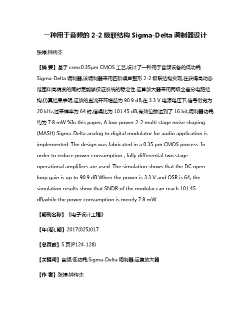
delta-sigma adc原理
delta-sigma adc原理Delta-Sigma ADC是一种常用的模数转换器,其原理基于Δ-Σ调制(Delta-Sigma Modulation)。
它应用广泛,特点是可实现高分辨率、低失真和高动态范围的模数转换。
1.简介Delta-Sigma ADC是将模拟信号转换为数字信号的一种技术。
它使用增量调制技术将输入信号转换为脉冲序列,再通过积分器形成模拟信号。
然后通过数字滤波器对模拟信号进行滤波,最后得到输出数字信号。
2.增量调制增量调制是Delta-Sigma ADC的核心部分。
它通过比较输入信号与量化器输出信号的差值,生成Δ-Σ调制的输出脉冲序列。
在增量调制中,使用一个比较器将输入信号与量化器输出信号进行比较。
当输入信号大于量化器输出信号时,比较器输出1;当输入信号小于量化器输出信号时,比较器输出-1。
这样,通过不断比较输入信号与量化器输出信号,就可以得到Δ-Σ调制的输出脉冲序列。
3.积分器在增量调制过程中,由于比较操作是离散的,会导致增量调制的输出脉冲序列带有高频成分。
为了消除这些高频成分,需要使用积分器将输出脉冲序列转换为模拟信号。
积分器通过对输出脉冲序列进行积分,得到与输入信号相关的模拟信号。
积分器可以使用电容器和运算放大器等元件来实现。
4.数字滤波器模拟信号经过积分器转换为数字信号后,仍然存在一些高频噪声。
为了滤除这些噪声,需要使用数字滤波器对数字信号进行滤波。
最常用的数字滤波器是低通滤波器,可以通过抽取和重插值的方式实现。
5.数据处理通过数字滤波器滤波后得到的输出数字信号可以用于后续的数据处理。
可以对其进行采样、量化和编码等操作,以得到最终的数字输出结果。
6.优势Delta-Sigma ADC具有以下优势:-高分辨率:通过增量调制和数字滤波器,可以实现较高的分辨率。
-低失真:增量调制和数字滤波器的特性可以降低噪声和失真。
-高动态范围:Delta-Sigma ADC可以实现比较大的动态范围,适用于高精度应用场景。
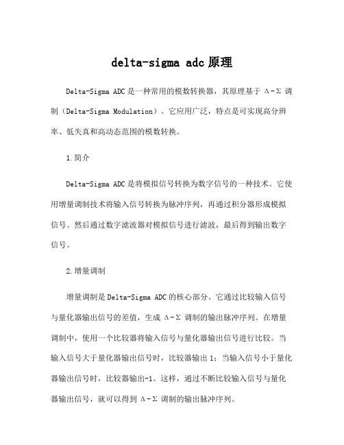
连续时间型ΣΔ调制器的系统级设计和建模方法
INT(扣端=南·兰(8) 1下石
其中,
GE一下堡尘垒L 二+2n·GBWRC I
艺△调制器的分辨率可以表示为一个关于过采 样比(oSR)、噪声整形阶数(L)以及内部量化器比
特数(Ⅳ)的函数表达式:
Dynami幽咒ge一号(学p一1)2∞∥1
(7) 式(7)实际成立的条件是环路的ⅣrF为(1一z_1)L。 尽管如此,式(7)依然对OSR、L以及Ⅳ的选取具有 一定的指导意义。为了充分地抑制量化噪声,使调制 器的分辨率达到大于12位的性能要求,根据式(7), 选取64倍过采样比、五阶噪声传递函数以及内部
数H咖(名)以及不归零反馈DAC波形后,为了得到
与H咖(2)冲激响应相同的连续时间型∑△调制器的
环路传递函数H咖(s),采用冲激不变法完成环路传
递函数z域到s域的变换。
另外,额外环路延时定义为量化器采样时钟的
有效边沿到反馈DAC波形输出之间的信号延时。考
虑到连续时间型乏△调制器特有的额外环路延时会
造成调制器性能的恶化甚至环路不稳定,设计采用
Ⅳb婶(2)=z一1·}+z一1·H7loop(Z) (4) V0
2·∑口j·Z--‘
H’JooP(2)=HIooP(名)·za0—Fal一——号-一 b。+∑b。·2一
萎f口;+, 一制订‘一毒以∥。
al
f11、
bo
b。+∑b。·名叫
ill
(5)
采用冲激不变法对图2(b)中H7Ioop(z)变换的过
Continuous time delta-sigma modulator
专利名称:Continuous time delta-sigma modulator 发明人:Oyama, Bert K.,Skones, William Marvin申请号:EP06025838.1申请日:20010612公开号:EP1760890B1公开日:20090520专利内容由知识产权出版社提供摘要:An analog-to-digital converter (170) that employs delta-sigma technology, and has particular use in a receiver for a wireless telecommunications system. The converter (170) includes a delta-sigma modulator (172), having a summing junction (180) that receives the analog input signal to be converted. A feedback from the output of a comparator (186) is subtracted from the analog input signal to generate a difference signal that is then filtered, amplified and applied to the comparator (186) for digital conversion. A sample and hold circuit (184) receives the difference signal and holds the signal for a predetermined period of time so that the input to the comparator (186) is stable. A differential limiting amplifier (188) is employed to make the high data rate output of the comparator (186) stable. The differential limiting amplifier (188) can be within the comparator (186) itself, or in the feedback path. In one embodiment, the differential amplifier (188) employs a Schottky diode clamp (226).申请人:NORTHROP GRUMMAN CORP地址:US国籍:US代理机构:Schmidt, Steffen J.更多信息请下载全文后查看。
AD转换分辨率的算法
AD转换分辨率的算法AD转换分辨率的算法是将模拟信号转换为数字信号的过程。
它通常包括采样和量化两个步骤。
采样是指周期性地测量模拟信号的幅值,并将其转换为数字形式。
量化是指将连续的模拟信号转换为离散的数字信号,即将其映射到一系列离散的数字值上。
在实际的AD转换中,常见的算法有以下几种:1. 逐次逼近法(successive approximation):这是一种常见的高速AD转换算法。
它通过不断比较转换结果与输入信号的大小关系,以找到最接近输入信号的数字值。
算法从最高位(MSB)开始,逐位逼近地确定每一位的值,直到找到最佳匹配值。
逐次逼近法的速度较快,但对于较高的分辨率可能需要较长的转换时间。
2. 闩锁比较法(flash method):这是一种用于高分辨率AD转换的算法。
它通过比较输入信号与一系列已知参考电压的大小关系来实现。
通常,该算法使用一组比较器,每个比较器都根据输入信号与不同的参考电压进行比较,并产生相应的输出。
然后,通过编码器将输出转换为数字信号。
闩锁比较法的速度非常快,但它需要大量的比较器。
3. Delta-Sigma调制(Delta-Sigma modulation):这是一种用于高精度AD转换的算法。
它将输入信号与一个标准信号进行高速调制,然后通过一个低通滤波器将调制后的信号转换为数字信号。
Delta-Sigma调制通过频率和时间域上的噪声压制来提高了转换精度。
这种算法适用于高分辨率和高动态范围的应用,但转换速度较慢。
总结起来,AD转换分辨率的算法主要包括逐次逼近法、闩锁比较法和Delta-Sigma调制。
这些算法各有特点,可以根据应用需求选择适合的算法。
- 1、下载文档前请自行甄别文档内容的完整性,平台不提供额外的编辑、内容补充、找答案等附加服务。
- 2、"仅部分预览"的文档,不可在线预览部分如存在完整性等问题,可反馈申请退款(可完整预览的文档不适用该条件!)。
- 3、如文档侵犯您的权益,请联系客服反馈,我们会尽快为您处理(人工客服工作时间:9:00-18:30)。
Continuous time D S modulation with PWM pre-coding and binary g m blocksA.Babaie Fishani and P.RomboutsA very simple technique to implement thefirst integrator of a continu-ous-time delta sigma modulator(CT-DSM)is presented.In theapproach,the CT-DSM is preceded by a pulse-width modulator toconvert the input signal to a pseudo-digital continuous time waveform.As a result,thefirst integrator of the DSM can be implemented with acapacitor and a switched current source,with inherent linearity.Toillustrate the concept,it has been applied to the design of a second-order CT-DSM in65nm CMOS technology.Introduction:Recently,various A/D conversion techniques that employ some kind of pulse width modulation(PWM)have been pre-sented[1–3].Such a PWM converts a baseband signal into a two-level continuous time waveform.Here,the information is stored in the transitions of this two-level waveform.If properly designed,no infor-mation is lost in this process.The two-level signal that comes out of the PWM can be easily processed by other circuit blocks.This way,a PWM is sometimes used in front of other blocks in the system’s signal path.This technique is referred to as PWM pre-coding.In prior work,PWM pre-coding has been used to linearise a VCO-based ADC [1].Alternatively,in[2]a time-to-digital converter was combined with PWM pre-coding to convert the PWM signal into the digital domain.The former approach[1]achieves afirst-order quantisation noise shaping,while the latter[2]exhibits no noise shaping at all.In this Letter we present a new method for utilising PWM pre-coding in the design of an ADC.In this work,the PWM is followed by a con-tinuous time DS modulator(CT-DSM),which,in contrast with previous work,can have quantisation noise-shaping of any arbitrary order.Proposed architecture:Fig.1shows the proposed ADC concept.Here, the input signal of the ADC isfirst applied to a PWM,then the output signal p(t)of the PWM is used to drive a switched current source. This switched current source can be viewed as a two-level transconduc-tor or a‘binary g m’.This binary g m is combined with a capacitor and these two simple elements together build an integrator which is used as thefirst integrator of a CT-DSM.The binary g m is very similar to the switched current source which is used as the feedback DAC.The combination of the switched current source and the capacitor of the first integrator also looks like the charge-pump structure,which is com-monly used as the loop-filter in aPLL.Fig.1Proposed architecture for linearising CT-DSMsThe main advantage of this approach over a conventional DSM is the simplicity in design and implementation of thefirst integrator in this approach.Thefirst integrator of a DSM has to satisfy several criteria, mostly with regard to linearity and noise,because all the non-idealities of this block directly corrupt the desired signal.For this reason,thefirst integrator of a DSM is usually responsible for most of the power con-sumption of the whole modulator and is the most challenging part of a DSM to be designed.In the proposed concept,on the other hand, thefirst integrator is implemented by a binary g m and a capacitor, which can be designed very easily.The pulse-width modulator is also an easy-to-design block[1].In its simplest version,it consists of a Schmitt-trigger and a passive loopfilter. However,a potential problem with a PWM signal is that it contains many harmonics of fc,the carrier frequency of the PWM.If these har-monics fall near integer multiples of fs,where fs is the clock frequency of the DSM,after sampling in the DSM loop,they might alias to the baseband and corrupt the desired signal[1].Fortunately,this problem is alleviated in this architecture,because anti-aliasingfiltering is one of the inherent qualities of a CT-DSM,and as the order of the modulator increases,the anti-aliasingfiltering will improve.As a result,the carrier frequency of the PWM can be chosen relatively freely in the sense that fs can be an integer multiple of fc while the aliasing effects are still modest. Obviously,the concept presented in Fig.1can easily be extended to multi-bit conversion by using a multi-bit quantiser and multiple switched current sources in the DAC.It is also clear that the proposed method can be applied to a CT-DSM of arbitrary order.Design example:To illustrate the effectiveness of the proposed concept, we have applied it to the design of a second-order CT-DSM for a bandwidth of16MHz with an OSR of64(corresponding to a clock fre-quency of around2GHz)in a standard65nm CMOS process.Fig.2 shows the corresponding circuit diagram.The upper part of the Figure is the pulse-width modulator.Conceptually,it consists of a feed-back loop with afirst-order passive loopfilter and a Schmitt-trigger.In the actual implementation,a tapered inverter buffer is added to make the rising and falling edges of the PWM signal steeper.As mentioned in the previous Section,the carrier frequency of the PWM,fc,does not need to be accurately controlled.Nevertheless,there are some considerations on the choice of fc.If fc is too close to the baseband,modulation sidebands may fall partially into the baseband.A high value of fc,on the other hand,increases the power consumption.Considering the targeted band-width,a carrier frequency of500MHz is chosen for the PWM.Fig.2Top-level schematic of design example ADC,consisting of pulse-width modulator and g m-C CT-DSMThe lower rectangle in Fig.2shows the CT-DSM that follows the PWM.Thefirst integrator is implemented by a binary g m and is driven by the pseudo-digital waveform p(t),as explained above.The requirements on the design of the second integrator,with transconductor g m2,are heavily relaxed because the non-ideal effects of this block are reduced by the high gain of thefirst integrator and are therefore negli-gible.For this block a simple source-degenerated differential-pair trans-conductor was chosen.The local feedback,implemented with the transconductor g mk,has a very small transconductance and has little impact on the overall linearity,noise or power of the modulator. The overall power consumption of the designed circuit is as low as 2.5mW from a single1.2V supply.The resulting output spectrum of a transistor level simulation of this circuit is shown in Fig.3.The corresponding SNR and SNDR are both equal to66dB for a16MHz bandwidth.As expected,the PWM carrier and its sidebands are visible around500MHz.These tones are safely away from the baseband and they can easily befiltered in the digital domain.The theoretical noise spectrum(calculated from the designed NTF)is also shown in the Figure.It matches the simulation very well,apart from the fact that the notch in the noise spectrum is ‘filled’in the simulated spectrum.This is owing to thefinite output impedance of the current sources in thefirst integrator,which can not easily be made arbitrarily large in this65nm CMOS technology (because of leakage effects).Owing to this,the DC-gain of thefirstELECTRONICS LETTERS13th September2012Vol.48No.19integrator is not infinite.If this effect is taken into account in the theor-etical plot,it matches the experiment nearly perfectly.106107108109−120−100−80−60−40−200frequency, Hzm a g n i t u d e , d B n o r m a l i s e dSNR = 66dB SNDR = 66dB OSR = 64basebandPWM carrierthird harmonic –78dBtheoretical predictionFig.3Transistor-level simulation result of output spectrum of design exampleConclusion:This Letter presents a simple technique to implement the first integrator of a CT-DSM with low complexity and power consump-tion.The approach uses a PWM to convert the input signal into a two-level signal so that a switched current source together with a capacitor can be used as the first integrator in a CT-DSM.The idea can beapplied to a CT-DSM arbitrary order that can have a single-bit as well as multi-bit quantiser.Acknowledgment:This work has been supported by the Fund for Scientific Research Flanders (FWO-Vlaanderen)Belgium.#The Institution of Engineering and Technology 20122August 2012doi:10.1049/el.2012.2697A.Babaie Fishani and P.Rombouts (CAS,ELIS,University of Gent,Gent,Belgium))E-mail:amir.babaiefishani@elis.ugent.be References1Hernandez,L.,Paton,S.,and Prefasi, E.:‘VCO-based sigma delta modulator with PWM precoding’,Electron Lett.,2011,49,(10),pp.558–5592Daniels,J.,Dehaene,W.,Steyaert,M.S.J.,and Wiesbuer,A.:‘A /D conversion using asynchronous delta-sigma modulation and time-to-digital conversion’,IEEE Trans.Circuits Syst.-I ,2010,57,(9),pp.2404–24103De Vuyst,B.,and Rombouts,P.:‘A 5-MHz 11-bit self-oscillating sigma delta modulator with a delay-based phase shifter in 0.025mm 2’,IEEE J.Solid-State Circuits ,2011,46,(8),pp.1919–1927ELECTRONICS LETTERS 13th September 2012Vol.48No.19。