TL062_07中文资料
TL062V中文资料

Table 1. Single Operational Amplifiers
IIB (µA) Max VIO (mV) Max TCVIO (µV/°C) (µV/ C) Typ IIO (nA) Max Avol (V/mV) Min BW (Av = 1) (MHz) Typ SR (Av = 1) (V/µs) Typ Supply Voltage (V) Min Max Description
元器件交易网
Amplifiers and Comparators
In Brief . . .
For over two decades, Motorola has continually refined and updated integrated circuit technologies, analog circuit design techniques and processes in response to the needs of the marketplace. The enhanced performance of newer operational amplifiers and comparators has come through innovative application of these technologies, designs and processes. Some early designs are still available but are giving way to the new, higher performance operational amplifier and comparator circuits. Motorola has pioneered in JFET inputs, low temperature coefficient input stages, Miller loop compensation, all NPN output stages, dual–doublet frequency compensation and analog “in–the–package” trimming of resistors to produce superior high performance operational amplifiers and comparators, operating in many cases from a single supply with low input offset, low noise, low power, high output swing, high slew rate and high gain–bandwidth product at reasonable cost to the customer. Present day operational amplifiers and comparators find applications in all market segments including motor controls, instrumentation, aerospace, automotive, telecommunications, medical, and consumer products. Page Operational Amplifiers . . . . . . . . . . . . . . . . . . . . . . . . . . . 4.1–2 Single . . . . . . . . . . . . . . . . . . . . . . . . . . . . . . . . . . . . . . 4.1–2 Dual . . . . . . . . . . . . . . . . . . . . . . . . . . . . . . . . . . . . . . . 4.1–3 Quad . . . . . . . . . . . . . . . . . . . . . . . . . . . . . . . . . . . . . . . 4.1–4 One Volt SMARTMOS™ Rail–to–Rail Dual Operational Amplifier . . . . . . . . . . . . . . . . . . . . . . . . . . . 4.1–6 High Frequency Amplifiers . . . . . . . . . . . . . . . . . . . . . . . 4.1–7 AGC . . . . . . . . . . . . . . . . . . . . . . . . . . . . . . . . . . . . . . . 4.1–7 Miscellaneous Amplifiers . . . . . . . . . . . . . . . . . . . . . . . . 4.1–8 Bipolar . . . . . . . . . . . . . . . . . . . . . . . . . . . . . . . . . . . . . 4.1–8 CMOS . . . . . . . . . . . . . . . . . . . . . . . . . . . . . . . . . . . . . 4.1–8 Comparators . . . . . . . . . . . . . . . . . . . . . . . . . . . . . . . . . . . 4.1–9 Single . . . . . . . . . . . . . . . . . . . . . . . . . . . . . . . . . . . . . . 4.1–9 Dual . . . . . . . . . . . . . . . . . . . . . . . . . . . . . . . . . . . . . . . 4.1–9 Quad . . . . . . . . . . . . . . . . . . . . . . . . . . . . . . . . . . . . . . . 4.1–9 Package Overview . . . . . . . . . . . . . . . . . . . . . . . . . . . . 4.1–10
TL062VD中文资料

DUAL
P SUFFIX PLASTIC PACKAGE CASE 626
Representative Schematic Diagram (Each Amplifier)
D SUFFIX PLASTIC PACKAGE CASE 751 (SO–8)
PIN CONNECTIONS
VCC Output 1 Inputs 1 Q7 VEE R4 Output
TL062 TL064
LOW POWER JFET INPUT OPERATIONAL AMPLIFIERS
SEMICONDUCTOR TECHNICAL DATA
• • • • • •
Low Input Bias Current: 5.0 pA High Gain Bandwidth: 2.0 MHz High Slew Rate: 6.0 V/µs High Input Impedance: 1012 Ω Large Output Voltage Swing: ±14 V Output Short Circuit Protection
NOTES: 1. Differential voltages are at the noninverting input terminal with respect to the inverting input terminal. 2. The magnitude of the input voltage must never exceed the magnitude of the supply or 15 V, whichever is less. 3. Power dissipation must be considered to ensure maximum junction temperature (TJ) is not exceeded. (See Figure 1.)
TL062 数据手册 (2)

DUAL
P SUFFIX PLASTIC PACKAGE CASE 626
Representative Schematic Diagram (Each Amplifier)
D SUFFIX PLASTIC PACKAGE CASE 751 (SO–8)
PIN CONNECTIONS
VCC Output 1 Inputs 1 Q7 VEE R4 Output
2
MOTOROLA ANALOG IC DEVICE DATA
TL062 TL064
DC ELECTRICAL CHARACTERISTICS (VCC = +15 V, VEE = –15 V, TA = Tlow to Thigh [Note 4], unless otherwise noted.)
Order this document by TL062/D
Low Power JFET Input Operational Amplifiers
These JFET input operational amplifiers are designed for low power applications. They feature high input impedance, low input bias current and low input offset current. Advanced design techniques allow for higher slew rates, gain bandwidth products and output swing. The commercial and vehicular devices are available in Plastic dual in–line and SOIC packages. • Low Supply Current: 200 µA/Amplifier
集成电路中英文对照

表面贴装集成电路SURFACE MOUNT INTEGRATED CIRCUITTYPE NO. FUNCTIONPIN TYPE NO. FUNCTIONPIN LM358 单电源通用型双运放8 UC3843 脉宽调制8/14 UPC1251 单电源通用型双运放(工业级) 8 UC3844 脉宽调制(开关电源) 14 LM741 单运放(通用型)8 LM317 三端可调(1.25~37V ) 8 UPC258 双运放(通用型)(工业级) 8 LM337 三端可调(1.25~37V ) 8 LM1458 双运放(通用型) 8 LM385 基准二极管(1.25V,2.5V) 8 LM4558 双运放(通用型) 8 78L05 三端稳压5V/100MA 3/8 LM324 单电源四运放14 78DS05 三端稳压5V/30MA(低压差) 3 UPC451 单电源四运放(工业级) 14 78L06 三端稳压6V/100MA 3 LM3403 单电源四运放 14 78L09 三端稳压9V/100MA 3 LM4741 单电源四运放 14 78L12 三端稳压12V/100MA 3 LF353 BI-GET 输入型双运放 8 79L05 三端稳压-5V/100MA 3 TL061 低功耗JFET 输入单远放 8 79L06 三端稳压-6V/100MA 3 TL062 低功耗JFET 输入双远放 8 79L09 三端稳压-9V/100MA 3 TL064 低功耗JFET 输入四远放 14 79L12 三端稳压-12V/100MA 3 TL072 低功耗JFET 输入双远放 8 78M05 三端稳压5V/500MA 3 TL074 低功耗JFET 输入四远放 14 78D05 三端稳压5V/500MA(低压差) 3 MC34074 高性能、单电源四远放 14 78M12 三端稳压12V/500MA 5 TL081 BEJFET 输入单远放 8 79M05 三端稳压-5V/500MA 3 TL082 BJ-JFET 输入双远放 8 79M12 三端稳压-12V500MA 3 TL084 BJ-JFET 输入四远放 14 A1600 单调MOSFET 陈列*8 16 UPC4572 高性能双远放 8 MC1403 精密基准二极管2.5V 8 UPC4574 高性能四远放 14 MC34063 开关电源 8 LM339 四电压比较器 14 MC34064 欠压传感电路 8 LM393 双电压比较器8 CD4001 二输入端四或非门 14 UPC277 双电压比较器(工业级) 8 CD4007 双互补对加倒相器 14 LM311 通用比较器(单) 8 CD4011 二输入端四与非门 14 LM319 高速双比较器8 CD4013 双D 触发器 14 LM2901 四电压比较器(-20℃~) 14 CD4016 四与向模拟开关 14 LM2902 单电源四运放(-20℃~) 14 CD4017 十进制计数/分配器 16 LM2903 双电压比较器(-20℃~) 8 CD4019 四与或选择器 16 LM2904 双电压比较器(-20℃~) 8 CD4021 八位静态移位寄存器 16 7660 电源变换器 8 CD4027 双J-K 触发器 16 LM386 功率放大 8 CD4028 BCD 十进制译码器 16 LM555 时基电路 8 CD4030 四异或门14 LMC555 COMS 时基电路 8 CD4040(HC) 四R/S 锁存器(与非三态) 14 LM556 双时基电路 14 CD4043 四R/S 锁存器(与非三态) 14 TLC556 CMOS 双时基电路 14 CD4046 锁相环16 TL431 可调三端 3/8 CD4049 六反相缓冲器/转换器 16 TL1451 双脉宽调制控制 16 CD4050(HC) 六同相缓冲器/转换器 16 D4990 串行I/O 实时时钟 16 CD4051 八选一模拟开关 16 OP07 低失调电压型运放 8 CD4052 双四选一模拟开关 16 OP27 低噪声低失调电压型运放 8 CD4053 三组二路双向模拟开关 16 OP37 低噪声低失调电压型运放(高速) 8 CD4060 14位串行二进制计数/分频/振荡 14 OP177 低失调电流型运放 8 CD4066 四双向模拟开关 14 7106 3 1/2DVM 用A/D 液晶 44 CD4069 六反相器 14 7107 3 1/2DVM 用A/D 数码管44 CD4070 四异或门 14 7117 3 1/2DVM 用A/D 数码管(HCLD ) 44 CD4071 二输入端四或门 14 D7554 4-Bit 单片机 20 CD4081 二输入端四或门14 MN1035 运放 8 CD4093 二输入端四与非史密特触发器 14 NJM318 高速单运放 8 CD4094 八位移位存储总线寄存器 16 TA76494 开关式稳压源 16 CD4512 八通道数据选择器 16 TL494 开关式稳压源 16 CD4516 二进制四位可逆计数器 16 MB3759 开关式稳压源 16 CD4518 双BCD 加法计数器 16 UC3842脉宽调制14CD4520双二进制加法计数器16表面贴装集成电路SURFACE MOUNT INTEGRATED CIRCUIT。
TLMW07说明书

TLMW07 全方位监测器1 产品简介该TLMW07是根据微波多普勒效应原理(也就是雷达基本原理)制作成的,可广泛应用于类似自动门控制开关、安全防范系统、A TM自动提款机的自动录像控制系统、以及其他需要自动感应控制的场所。
这种探测方式与其它探测方式相比具有如下的优点:1、非接触探测;2、不受温度、湿度、噪声、气流、尘埃、光线等影响,适合恶劣环境;3、抗射频干扰能力强;4、输出功率仅有5mW,对人体构不成危害。
安装及接线简单。
这和市场上常见的简易型微波感应控制器相比较,因为采用专用的微处理集成器,不但检测灵敏度度高,探测范围宽,而且工作非常可靠,误报率极低,能在-25~+45度的温度范围内稳定工作。
TLMW07开关量信号可设置,探测灵敏度、距离可调,报警时间、距离可设置,探测方向可调,穿透性能好。
输出周期为2秒-180秒可设置。
2 应用领域1.A TM、自动柜员机、A TM监控2.家庭3.商店4.工厂5. 宾馆、6.机关、7.其他防盗等安防装置8.A TM自动提款机3 产品特征电源:DC 6V~12V,微波探头感应有效距离:0~ 7M,模块尺寸:48mm*30mm*12mm,天线采用软质材料制成。
控制器的外形右图所示,面板上设置有灵敏度调整孔,可以使监控距离在0~7米范围内可调,可以通过电路板的可调电阻来调节探测距离。
此微波感应控制器工作非常可靠,一般没有误报,是以往红外线、超声波、热释电元件组成的报警电路以及常规微波电路所无法比拟的,是目前用于安全防范和自动监控以及自动感应的最佳产品。
4典型应用下面介绍运用高可靠微波感应控制器制作的实用电子装置,它们的共同特点是线路新颖简单,实用性强,制作容易,性价比高。
一、自动感应灯灯可以自动识别周围环境光的亮度,能够实现人来灯亮,人走灯灭,不会误动作,可靠性高,而且电路的工作状态不会受自身灯光的干扰,可以广泛地运用在走廊、卫生间、庭院等场合实现自动照明。
二、使用于A TM机器及其他自动化控制设备当微波探测器感应到人体后,将在信号线输出一个高电平信号,A TM主控机检测到这个信号后,将打开摄像机并将录像指令传给硬盘录像机,如果是晚上,还可以同步打开红外补光灯做摄像机的辅助照明。
SGL-0622Z;中文规格书,Datasheet资料

Caution! ESD sensitive device.
Exceeding any one or a combination of the Absolute Maximum Rating conditions may cause permanent damage to the device. Extended application of Absolute Maximum Rating conditions to the device may reduce device reliability. Specified typical performance or functional operation of the device under Absolute Maximum Rating conditions is not implied.
1950 MHz
26.1
12.8 12.1 34.8 1.78
2440 MHz
23.0 -12.0
1.5
12.0 14.0 32.0 2.01
4
10.0 22.0 29.0 2.81
2 of 6 /
dB
34.6
34.9
34.4
32.8
28.5
Input Third Order Intercept Point, dBm IIP3
-13.0
Output at 1dB Compression,
dBm
2.7
5.3
P1dB
Input Return Loss
dB
15.1
20.0
12.6
16.0
14.3
Output Return Loss
Device Operating Current
2A07-T中文资料

e 32A01 - 2A072.0A RECTIFIERFeaturesMaximum Ratings and Electrical Characteristics@ T A = 25°C unless otherwise specified·Diffused Junction·High Current Capability and Low Forward Voltage Drop ·Surge Overload Rating to 70A Peak·Lead Free Finish, RoHS Compliant (Note 3)Mechanical Data·Case: DO-15·Case Material: Molded Plastic. UL Flammability Classification Rating 94V-0·Moisture Sensitivity: Level 1 per J-STD-020C·Terminals: Finish – Bright Tin. Solderable per MIL-STD-202,Method 208·Polarity: Cathode Band ·Marking: Type Number·Weight: 0.4 grams (approximate)Single phase, half wave, 60Hz, resistive or inductive load.For capacitive load, derate current by 20%.Notes: 1. Leads maintained at ambient temperature at a distance of 9.5mm from the case.2. Measured at 1.0 MHz and Applied Reverse Voltage of 4.0V DC.3. RoHS revision 13.2.2003. Glass and High Temperature Solder Exemptions Applied, see EU Directive Annex Notes 5 and 7.0.010.11.0100.40.8 1.21.6I ,I N S T A N T A N E O U S F O R W A R D C U R R E N T (A )F VF,INSTANTANEOUS FORWARD VOLTAGE (V)Fig.2Typical Forward Characteristics1.0101001.010100C ,T O T A L C A P A C I T A N C E (p F )T V ,REVERSE VOLTAGE (V)Fig.4Typical Total CapacitanceR 02.5I ,A V E R A G E F O R W A R D R E C T I F I E D C U R R E N T (A )O T ,AMBIENT TEMPERATURE (ºC)Fig.1Forward Current Derating CurveA 2550751001251501752000.51.01.52.0110100I ,P E A K F O R W A R D S U R G E C U R R E N T (A )F S M NUMBER OF CYCLES AT 60HzFig.3Max Non-Repetitive Peak Fwd SurgeCurrent03060754515Ordering InformationNotes:4.For packaging details, visit our website at /datasheets/ap02008.pdf.(Note 4)IMPORTANT NOTICEDiodes Incorporated and its subsidiaries reserve the right to make modifications,enhancements,improvements,corrections or other changes without further notice to any product herein.Diodes Incorporated does not assume any liability arising out of the application or use of any product described herein;neither does it convey any license under its patent rights,nor the rights of others.The user of products in such applications shall assume all risks of such use and will agree to hold Diodes Incorporated and all the companies whose products are represented on our website,harmless against all damages.LIFE SUPPORTDiodes Incorporated products are not authorized for use as critical components in life support devices or systems without the expressed written approval of the President of Diodes Incorporated.。
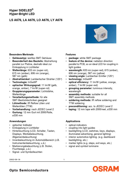
LOA676中文资料
LS A676, LA A676, LO A676, LY A676Hyper SIDELED ®Hyper-Bright LED2002-09-181Besondere Merkmale•Geh äusetyp: wei ßes SMT Geh äuse•Besonderheit des Bauteils: Abstrahlung parallel zur Platine, deshalb ideal zur Einkopplung in Lichtleiter•Wellenl änge: 633 nm (super-rot), 615nm (amber), 606 nm (orange), 587nm (gelb)•Abstrahlwinkel: Lambertscher Strahler (120°)•Technologie: InGaAlP•optischer Wirkungsgrad: 11 lm/W (gelb, orange, amber), 7 lm/W (super-rot)•Gruppierungsparameter: Lichtst ärke, Wellenl änge•Verarbeitungsmethode: f ür alle SMT-Best ücktechniken geeignet •L ötmethode: IR Reflow L öten und Wellenl öten (TTW)•Vorbehandlung: nach JEDEC Level 2•Gurtung: 12 mm Gurt mit 2000/Rolle, ø330mm Anwendungen•optischer Indikator•Einkopplung in Lichtleiter•Hinterleuchtung (LCD, Schalter, Tasten, Displays, Werbebeleuchtung, Allgemeinbeleuchtung)•Innenbeleuchtung im Automobilbereich (z.B. Instrumentenbeleuchtung, u.ä.)•Markierungsbeleuchtung (z.B. Stufen, Fluchtwege, u.ä.)•Signal- und SymbolleuchtenFeatures•package: white SMT package•feature of the device: radiation directionparallel to PCB, so an ideal LED for coupling in light guides•wavelength: 633 nm (super-red), 615 (amber), 606 nm (orange), 587 nm (yellow)•viewing angle: Lambertian Emitter (120°)•technology: InGaAlP•optical efficiency: 11 lm/W (yellow, orange, amber), 7 lm/W (super-red)•grouping parameter: luminous intensity, wavelength•assembly methods: suitable for all SMT assembly methods•soldering methods: IR reflow soldering and TTW soldering•preconditioning: acc. to JEDEC Level 2•taping: 12 mm tape with 2000/reel, ø330mmApplications•optical indicators•coupling into light guides•backlighting (LCD, switches, keys, displays, illuminated advertising, general lighting)•interior automotive lighting. (e.g. dashboard backlighting, etc.)•marker lights (e.g. steps, exit ways, etc.)•signal and symbol luminaire2002-09-182Anm.:-1 gesamter Farbbereich (siehe Seite 4)-24 gesamter Farbbereich, Lieferung in Einzelgruppen (siehe Seite 5)-26 gesamter Farbbereich, Lieferung in Einzelgruppen (siehe Seite 5)Die Standardlieferform von Serientypen beinhaltet eine untere bzw. eine obere Familiengruppe,die aus nur 3bzw.4 Halbgruppen besteht. Einzelne Halbgruppen sind nicht erhältlich.In einer Verpackungseinheit /Gurt ist immer nur eine Halbgruppe enthalten.Note:-1 Total color tolerance range (please see page 4)-24 Total color tolerance range, delivery in single groups (please see page 5)-26 Total color tolerance range, delivery in single groups (please see page 5)The standard shipping format for serial types includes a lower or upper family group of 3or 4individual groups. Individual half groups are not available.No packing unit /tape ever contains more than one luminous intensity half group.TypTypeEmissions-farbe Color of EmissionFarbe derLichtaustritts-fl ächeColor of the Light Emitting AreaLichtst ärkeLuminous Intensity I F = 20mA I V (mcd)LichtstromLuminous FluxI F = 20mA ΦV (mlm)BestellnummerOrdering CodeLS A676-N2P2-1LS A676-P2R1-1super-red colorless clear 35.5 ...71.056.0 ...140.0150 (typ.)280 (typ.)Q62703Q5074Q62703Q5075LA A676-Q1R1-1LA A676-R1S2-1amber colorless clear 71.0 ...140.0112.0 ...280.0310 (typ.)560 (typ.)Q62703Q4972Q62703Q4973LO A676-Q1R1-24LO A676-R1S2-24orange colorless clear 71.0 ...140.0112.0 ...280.0310 (typ.)560 (typ.)Q62702Q5032Q62702Q5033LY A676-P2Q2-26LY A676-Q2S1-26yellowcolorless clear56.0 ...112.090.0 ...224.0240 (typ.)440 (typ.)Q62703Q5111Q62703Q5112Grenzwerte Maximum RatingsBezeichnung Parameter SymbolSymbolWerteValuesEinheitUnitLS, LO, LA LYBetriebstemperatur Operating temperature range Top– 55 … + 100°CLagertemperaturStorage temperature range Tstg– 55 … + 100°CSperrschichttemperatur Junction temperature Tj+ 100°CDurchlassstrom Forward current IF30mAStoßstromSurge currentt≤ 10 µs, D = 0.005IFM10.2ASperrspannung1) Reverse voltage VR12VLeistungsaufnahme Power consumption Ptot80mWWärmewiderstand Thermal resistanceSperrschicht/UmgebungJunction/ambientSperrschicht/LötpadJunction/solder pointMontage auf PC-Board FR 4 (Padgröße ≥ 16mm2) mounted on PC board FR 4 (pad size ≥ 16 mm 2)Rth JARth JS530300K/WK/W1)für kurzzeitigen Betrieb geeignet / suitable for short term application2002-09-1832002-09-184Kennwerte (T A = 25 °C)Characteristics Bezeichnung ParameterSymbol SymbolWerte Values Einheit UnitLSLA LO LY Wellenl änge des emittierten Lichtes (typ.)Wavelength at peak emission I F = 20mAλpeak645622610591nmDominantwellenl änge 1)(typ.)Dominant wavelength 1)I F = 20mAλdom633± 6615± 6606–6/+3587–7/+8nmSpektrale Bandbreite bei 50 % I rel max (typ.)Spectral bandwidth at 50 % I rel max I F = 20mA∆λ16161615nmAbstrahlwinkel bei 50 % I V (Vollwinkel)(typ.)Viewing angle at 50 % I V 2ϕ120120120120Grad deg.Durchlassspannung 2)(typ.)Forward voltage 2)(max.)I F = 20mA V F V F 2.02.4 2.02.4 2.02.4 2.02.4V VSperrstrom(typ.)Reverse current (max.)V R = 12 VI R I R 0.01100.01100.01100.0110µA µATemperaturkoeffizient von λpeak (typ.)Temperature coefficient of λpeak I F = 20mA; –10°C ≤ T ≤ 100°C TC λpeak0.140.130.130.13nm/KTemperaturkoeffizient von λdom (typ.)Temperature coefficient of λdom I F = 20mA; –10°C ≤ T ≤ 100°C TC λdom0.050.060.070.10nm/KTemperaturkoeffizient von V F (typ.)Temperature coefficient of V F I F = 20mA; –10°C ≤ T ≤ 100°C TC V– 2.0– 1.8– 1.7– 2.5mV/KOptischer Wirkungsgrad (typ.)Optical efficiency I F = 20mAηopt7111111lm/W1)Wellenl ängen werden mit einer Stromeinpr ägedauer von 25ms und einer Genauigkeit von ±1nm ermittelt.Wavelengths are tested at a current pulse duration of 25ms and a tolerance of ±1nm.2)Spannungswerte werden mit einer Stromeinpr ägedauer von 1ms und einer Genauigkeit von ±0,1V ermittelt.Voltages are tested at a current pulse duration of 1ms and a tolerance of ±0.1V.2002-09-185Helligkeitswerte werden mit einer Stromeinpr ägedauer von 25ms und einer Genauigkeit von ±11% ermittelt.Luminous intensity is tested at a current pulse duration of 25ms and a tolerance of ±11%.1)Wellenl ängengruppen / Wavelength groupsGruppe Group yellow orange Einheit Unit min.max.min.max.2580583600603nm 3583586603606nm 4586589606609nm 5589592nm 6592595nmHelligkeits-GruppierungsschemaLuminous Intensity Groups LichtgruppeLuminous Intensity Group Lichtst ärkeLuminous Intensity I V (mcd)Lichtstrom Luminous Flux ΦV (mlm)N2P1P2Q1Q2R1R2S1S235.5 ...45.045.0 ...56.056.0 ...71.071.0 ...90.090.0 ...112.0112.0 ...140.0140.0 ...180.0180.0 ...224.0224.0 ...280.0120 (typ.)150 (typ.)190 (typ.)240 (typ.)300 (typ.)380 (typ.)480 (typ.)600 (typ.)760 (typ.)Gruppenbezeichnung auf Etikett Group Name on Label Beispiel: P2-3Example: P2-3LichtgruppeLuminous Intensity Group Halbgruppe Half Group Wellenl änge Wavelength P23Relative spektrale Emission I rel = f (λ), T A = 25 °C, I F = 20mA Relative Spectral EmissionV(λ) = spektrale AugenempfindlichkeitStandard eye response curveAbstrahlcharakteristik I rel = f (ϕ)2002-09-186Durchlassstrom I F = f (V F)Forward CurrentMaximal zulässiger Durchlassstrom I F = f (T) Max. Permissible Forward Current Relative Lichtstärke I V/I V(20mA) = f (I F) Relative Luminous IntensityV V(25 °C)ARelative Luminous Intensity2002-09-187Zulässige Impulsbelastbarkeit I F = f (t p) Permissible Pulse Handling Capability Duty cycle D = parameter, T A = 25 °CF p Permissible Pulse Handling Capability Duty cycle D = parameter, T A = 85 °CZulässige Impulsbelastbarkeit I F = f (t p) Permissible Pulse Handling Capability Duty cycle D = parameter, T A = 25 °CF p Permissible Pulse Handling Capability Duty cycle D = parameter, T A = 85 °C2002-09-188MaßzeichnungPackage OutlinesMaße werden wie folgt angegeben: mm (inch) / Dimensions are specified as follows: mm (inch). Kathodenkennung:abgeschrägte EckeCathode mark:bevelled edgeGewicht / Approx. weight:40 mg2002-09-189Lötbedingungen Vorbehandlung nach JEDEC Level 2 Soldering Conditions Preconditioning acc. to JEDEC Level 2 IR-Reflow Lötprofil(nach IPC 9501)IR Reflow Soldering Profile(acc. to IPC 9501)2002-09-1810Wellenlöten (TTW)(nach CECC 00802)TTW Soldering(acc. to CECC 00802)2002-09-1811Empfohlenes Lötpaddesign Wellenlöten (TTW)Recommended Solder Pad TTW SolderingMaße werden wie folgt angegeben: mm (inch) / Dimensions are specified as follows: mm (inch) 2002-09-1812Empfohlenes Lötpaddesign IR Reflow LötenRecommended Solder Pad IR Reflow SolderingMaße werden wie folgt angegeben: mm (inch) / Dimensions are specified as follows: mm (inch). Gurtung / Polarität und Lage Verpackungseinheit2000/Rolle, ø330 mm Method of Taping / Polarity and Orientation Packing unit2000/reel, ø330 mmMaße werden wie folgt angegeben: mm (inch) / Dimensions are specified as follows: mm (inch)2002-09-18132002-09-1814Published by OSRAM Opto Semiconductors GmbH Wernerwerkstrasse 2, D-93049 Regensburg © All Rights Reserved.Attention please!The information describes the type of component and shall not be considered as assured characteristics.All typical data and graphs are basing on representative samples, but don ’t represent the production range. If requested, e.g. because of technical improvements, these typ. data will be changed without any further notice.Terms of delivery and rights to change design reserved. Due to technical requirements components may contain dangerous substances. For information on the types in question please contact our Sales Organization.If printed or downloaded, please find the latest version in the Internet.PackingPlease use the recycling operators known to you. We can also help you – get in touch with your nearest sales office.By agreement we will take packing material back, if it is sorted. You must bear the costs of transport. For packing material that is returned to us unsorted or which we are not obliged to accept, we shall have to invoice you for any costs incurred.Components used in life-support devices or systems must be expressly authorized for such purpose! Critical components 1 may only be used in life-support devices or systems 2 with the express written approval of OSRAM OS.1A critical component is a component used in a life-support device or system whose failure can reasonably be expected to cause the failure of that life-support device or system, or to affect its safety or the effectiveness of that device or system.2Life support devices or systems are intended (a) to be implanted in the human body, or (b) to support and/or maintain and sustain human life. If they fail, it is reasonable to assume that the health of the user may be endangered.Revision History:2002-09-18Date of changePrevious Version:2002-08-19Page Subjects (major changes since last revision)12recommended solder pad (TTW soldering)4value (wavelength amber/yellow 5wavelength groups2wavelength grouping for yellow and orange 14annotations2002-07-254value (TC λdom from 0.04 to 0.05nm/K)2002-07-2513recommended solder pad (IR reflow soldering)2002-08-013, 4value (reverse voltage from 3V to 12V)2002-09-18。
- 1、下载文档前请自行甄别文档内容的完整性,平台不提供额外的编辑、内容补充、找答案等附加服务。
- 2、"仅部分预览"的文档,不可在线预览部分如存在完整性等问题,可反馈申请退款(可完整预览的文档不适用该条件!)。
- 3、如文档侵犯您的权益,请联系客服反馈,我们会尽快为您处理(人工客服工作时间:9:00-18:30)。
Parameter
TL062M
TL062I
TL062C
Unit
Min Typ Max Min Typ Max Min Typ Max
Vio DVio
Iio Iib
Input offset voltage (RS = 50Ω) Tamb = +25°C Tmin ≤ Tamb ≤ Tmax
Temperature coefficient of input offset voltage (RS = 50Ω)
Absolute maximum ratings and operating conditions
Table 1. Absolute maximum ratings
Symbol
Parameter
VCC Vi Vid Ptot
Tstg
Rthja
Supply voltage (1) Input voltage (2) Differential input voltage(3)
1.5 3.5
1.5 3.5
V/μs
4/14
元器件交易网
TL062
Electrical characteristics
Table 3. Symbol
VCC = ±15V, Tamb = +25°C (unless otherwise specified) (continued)
the ground.
Table 2. Symbol
Operating conditions Parameter
TL062M, AM, BM TL062I, AI, BI TL062C, AC, BC Unit
VCC Supply voltage range
6 to 36
V
Toper Operating free-air temperature range
Vቤተ መጻሕፍቲ ባይዱ1/Vo2
Av = 100, Tamb = 25°C
120
120
120
dB
Total power consumption
PD
Tamb = +25°C, no load, no signal
6 7.5
6 7.5
6 7.5 mW
Slew rate
SR
1.5 3.5
Vi=10V, RL = 10kΩ, CL= 100pF, Av=1
7 - Output 2 8 - VCC+
July 2007
Rev 2
1/14
14
元器件交易网
Schematic diagram
1
Schematic diagram
Figure 1. Schematic diagram
TL062
VCC
Inverting Input
2. The magnitude of the input voltage must never exceed the magnitude of the supply voltage or 15 volts, whichever is less.
3. Differential voltages are the non-inverting input terminal with respect to the inverting input terminal.
RS = 50Ω
Supply voltage rejection ratio SVR
RS = 50Ω
80 95
80 95
70 95
dB
Supply current, no load
ICC
Tamb = +25°C, no load, no signal
200 250
200 250
200 250 μA
Channel separation
Input offset current (1)
Tamb = +25°C Tmin ≤ Tamb ≤ Tmax
Input bias current (1)
Tamb = +25°C Tmin ≤ Tamb ≤ Tmax
Vicm Input common mode voltage range
36 15
10
Vopp
Tamb = +25°C
20 27
20 27
20 27
V
Tmin ≤ Tamb ≤ Tmax
20
20
20
Large signal voltage gain
Avd
RL = 10kΩ, Vo = ±10V, Tamb = +25°C
Tmin ≤ Tamb ≤ Tmax
4
6
4
46 4
36 3
V/mV
Description
The TL062, TL062A and TL062B are high-speed JFET input single operational amplifiers. Each of these JFET input operational amplifiers incorporates well matched, high-voltage JFET and bipolar transistors in a monolithic integrated circuit.
-55 to +125
-40 to +105
0 to +70
°C
3/14
元器件交易网
Electrical characteristics
3
Electrical characteristics
TL062
Table 3. Symbol
VCC = ±15V, Tamb = +25°C (unless otherwise specified)
combinations with other pins floating. 8. Machine model: a 200pF cap is charged to the specified voltage, then discharged directly between two pins of the device
元器件交易网
TL062
Low power JFET dual operational amplifiers
Features
■ Very low power consumption : 200µA ■ Wide common-mode (up to VCC+) and
differential voltage ranges ■ Low input bias and offset currents ■ Output short-circuit protection ■ High input impedance JFET input stage ■ Internal frequency compensation ■ Latch up free operation ■ High slew rate : 3.5V/µs
GBP Ri
Gain bandwidth product Tamb = +25°C, RL =10kΩ, CL = 100pF Input resistance
1 1012
1 1012
1 1012
MHz Ω
Common mode rejection ratio
CMR
80 86
80 86
70 76
dB
4. The output may be shorted to ground or to either supply. Temperature and/or supply voltages must be limited to ensure that the dissipation rating is not exceeded.
Kov
Vi = 20mV, RL = 10kΩ, CL = 100pF,
10
10
10
%
Av = 1
Equivalent input noise voltage
en
RS = 100Ω, f = 1kHz
42
42
42
Parameter
TL062M
TL062I
TL062C
Unit
Min Typ Max Min Typ Max Min Typ Max
Rise time
tr
Vi = 20mV, RL = 10kΩ,
CL = 100pF, Av = 1
0.2
0.2
0.2
μs
Overshoot factor (see Figure 15)
±18
V
±15
V
±30
V
680
mW
Infinite
-65 to +150
-65 to +150
-65 to +150
°C
125
°C/W
85
Rthjc ESD
Thermal resistance junction to case(5) (6)
SO-8 DIP8
HBM: human body model(7)
5. Short-circuits can cause excessive heating and destructive dissipation. 6. Rth are typical values. 7. Human body model: 100pF discharged through a 1.5kΩ resistor between two pins of the device, done for all couples of pin