LM73CIMK-1中文资料
LM331中文资料 中文手册 芯片中文资料 芯片中文手册

电压-频率变换器LM331LM331是美国NS公司生产的性能价格比较高的集成芯片。
LM331可用作精密的频率电压(F/V)转换器、A/D转换器、线性频率调制解调、长时间积分器以及其他相关的器件。
LM331为双列直插式8脚芯片,其引脚如图3所示。
LM331内部有(1)输入比较电路、(2)定时比较电路、(3)R-S触发电路、(4)复零晶体管、(5)输出驱动管、(6)能隙基准电路、(7)精密电流源电路、(8)电流开关、(9)输出保护点路等部分。
输出管采用集电极开路形式,因此可以通过选择逻辑电流和外接电阻,灵活改变输出脉冲的逻辑电平,从而适应TTL、DTL和CMOS 等不同的逻辑电路。
此外,LM331可采用单/双电源供电,电压范围为4~40V,输出也高达40V。
引脚1(PIN1)为电流源输出端,在f0(PIN3)输出逻辑低电平时,电流源IR输出对电容CL充电。
引脚2(PIN2)为增益调整,改变RS的值可调节电路转换增益的大小。
引脚3(PIN3)为频率输出端,为逻辑低电平,脉冲宽度由Rt和Ct决定。
引脚4(PIN4)为电源地。
引脚5(PIN5)为定时比较器正相输入端。
引脚6(PIN6)为输入比较器反相输入端。
引脚7(PIN7)为输入比较器正相输入端。
引脚8(PIN8)为电源正端。
LM331频率电压转换器V/F变换和F/V变换采用集成块LM331,LM331是美国NS公司生产的性能价格比较高的集成芯片,可用作精密频率电压转换器用。
LM331采用了新的温度补偿能隙基准电路,在整个工作温度范围内和低到4.0V电源电压下都有极高的精度。
同时它动态范围宽,可达100dB;线性度好,最大非线性失真小于0.01%,工作频率低到0.1Hz时尚有较好的线性;变换精度高,数字分辨率可达12位;外接电路简单,只需接入几个外部元件就可方便构成V/F或F/V等变换电路,并且容易保证转换精度。
图2是由LM331组成的电压频率变换电路,LM331内部由输入比较器、定时比较器、R-S触发器、输出驱动、复零晶体管、能隙基准电路和电流开关等部分组成。
CD73NP-271KC资料

仕 様 書形 名CD731.外形1-1.寸法図(mm)* 公差のない寸法は、参考値とする。
1-2.捺印表示例 1-3.推奨ランド寸法(mm)2.コイル仕様2-1.端子接続図(裏面図)7.0±0.3 3.5±0.57.0φ7.8φ7.8±0.32.1製造密番頭部直捺印捺印位置不定電極部compliance Cd:Max.0.01wt%others:Max.0.1wt%RoHS1仕 様 書形 名CD732-2.電気的特性 NO.品 名 ※1表示インダクタンス[以内] ※2D.C.R. (mΩ) [以下] (at 20℃) ※3定格電流 (A) ※4 S.R.F.(MHz) [参考値]スミダコード01 CD73NP-1ØØMC 4730-006802 CD73NP-1ØØMB 100M 10μH±20% 80.3(61.8) 1.44 38.74730-008903 CD73NP-12ØMC 4730-006904 CD73NP-12ØMB 120M 12μH±20% 89.7(69.0) 1.39 34.84730-009005 CD73NP-15ØMC 4730-007006 CD73NP-15ØMB 150M 15μH±20% 104(80.3) 1.24 31.74730-009107 CD73NP-18ØMC 4730-007108 CD73NP-18ØMB 180M 18μH±20% 111(85.0) 1.12 28.14730-009209 CD73NP-22ØMC 4730-007210 CD73NP-22ØMB 220M 22μH±20% 129(99.2) 1.07 26.34730-009311 CD73NP-27ØMC 4730-007312 CD73NP-27ØMB 270M 27μH±20% 153(118) 0.94 23.74730-009413 CD73NP-33ØMC 4730-007414 CD73NP-33ØMB 330M 33μH±20% 170(131) 0.85 21.34730-009515 CD73NP-39ØMC 4730-007616 CD73NP-39ØMB 390M 39μH±20% 217(167) 0.74 17.44730-009617 CD73NP-47ØMC 4730-007718 CD73NP-47ØMB 470M 47μH±20% 252(194) 0.68 15.54730-009819 CD73NP-56ØKC 4730-007820 CD73NP-56ØKB 560K 56μH±10% 282(217) 0.64 13.54730-009921 CD73NP-68ØKC 4730-007922 CD73NP-68ØKB 680K 68μH±10% 332(255) 0.59 11.94730-010023 CD73NP-82ØKC 4730-008024 CD73NP-82ØKB 820K 82μH±10% 406(312) 0.54 11.44730-010125 CD73NP-1Ø1KC 4730-008126 CD73NP-1Ø1KB 101K 100μH±10% 481(370) 0.51 10.54730-010227 CD73NP-121KC 4730-008228 CD73NP-121KB 121K 120μH±10% 536(412) 0.49 9.84730-010329 CD73NP-151KC 4730-008330 CD73NP-151KB 151K 150μH±10% 755(581) 0.40 8.54730-010431 CD73NP-181KC 4730-008432 CD73NP-181KB 181K 180μH±10% 1022(786) 0.36 7.94730-010533 CD73NP-221KC 4730-008534 CD73NP-221KB 221K 220μH±10% 1200(923) 0.31 7.14730-010635 CD73NP-271KC 4730-008736 CD73NP-271KB 271K 270μH±10% 1306(1045) 0.29 6.24730-010737 CD73NP-331KC 4730-008838 CD73NP-331KB 331K 330μH±10% 1495(1196) 0.28 5.64730-0109※1: 品名表示の区分(1) リール梱包の場合: CD73NP-XXXXC (2) 箱梱包の場合: CD73NP-XXXXB※2:測定周波数 L 10μH ~ 82μH ; at 2.52 MHz 100μH ~330μH ; at 1 kHz ※3:( )内は、標準値とする。
LM10线性磁编码器系统数据表说明书
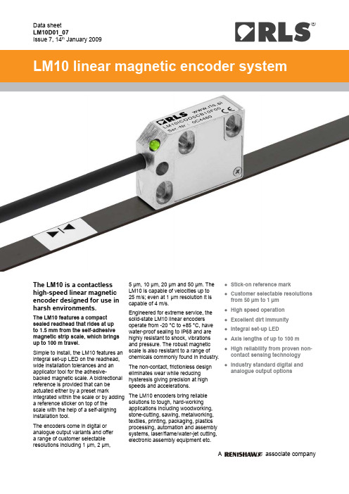
®Data sheet LM10D01_07Issue 7, 14thJanuary 2009The LM10 is a contactless high-speed linear magnetic encoder designed for use in harsh environments.The LM10 features a compact sealed readhead that rides at up to 1.5 mm from the self-adhesive magnetic strip scale, which brings up to 100 m travel.Simple to install, the LM10 features an integral set-up LED on the readhead, wide installation tolerances and an applicator tool for the adhesive-backed magnetic scale. A bidirectional reference is provided that can be actuated either by a preset markintegrated within the scale or by adding a reference sticker on top of thescale with the help of a self-aligninginstallation tool.The encoders come in digital or analogue output variants and offer a range of customer selectable resolutions including 1 µm, 2 µm,5 µm, 10 µm, 20 µm and 50 µm. The LM10 is capable of velocities up to 25 m/s; even at 1 µm resolution it is capable of 4 m/s.Engineered for extreme service, thesolid-state LM10 linear encoders operate from -20 °C to +85 °C, have water-proof sealing to IP68 and are highly resistant to shock, vibrations and pressure. The robust magnetic scale is also resistant to a range of chemicals commonly found in industry.The non-contact, frictionless design eliminates wear while reducinghysteresis giving precision at high speeds and accelerations.The LM10 encoders bring reliablesolutions to tough, hard-working applications including woodworking, stone-cutting, sawing, metalworking, textiles, printing, packaging, plasticsprocessing, automation and assembly systems, laser/flame/water-jet cutting, electronic assembly equipment etc.Stick-on reference mark●Customer selectable resolutions ●from 50 µm to 1 µm High speed operation ●Excellent dirt immunity ●Integral set-up LED ●Axis lengths of up to 100 m ●High reliability from proven non- ●contact sensing technology Industry standard digital and ●analogue output optionsData sheetLM10D01_07Dimensions and tolerances in mm.LM10 dimensionsLM10 installation tolerancesRide height0.1 - 1.5 mm®Maximum measuring length 50 m (100 m special order)Pole length2 mmAvailable resolution for digital outputs 1 µm, 2 µm, 5 µm, 10 µm, 20 µm and 50 µm Sinusoidal period length 2 mmMaximum speedFor analogue voltage and analogue current output: 25 m/s Sensor/magnetic scale gap With periodic or machined reference: 0.1 to 1.5 mm With stick-on reference: 0.5 to 1.5 mm Error band±40 µm at 20 °C Linear expansion coefficient ~ 17 × 10-6/KRepeatability Better than unit of resolution for movement in the same direction Hysteresis*< 3 µm up to 0.2 mm ride height Sub divisional error±3.5 µm for < 0.7 mm ride height (to ensure SDE remains under ±3.5 µm order option 01 that provides alarm and red LED at 0.7 mm ride height)±7.5 µm for 1 mm ride height Cable PUR high flexible cable, drag-chain compatible, double-shielded 8 × 0.05 mm 2; durability: 20 million cycles at 20 mm bend radiusReadhead (1 m cable, no connector) 56.4 g, Magnetic scale (1 m) 60 g, Cover foil (1 m) 3.5 gPower supply4.7 V to 7 V – reverse polarity protected; voltage on readhead Power consumption (without any load)< 30 mA for digital output type < 50 mA for analogue output types Voltage drop over cable 13 mV/m – without load 54 mV/m – with 120 Ω loadOutput signalsDigital – Open Collector NPN, Differential RS422, short circuit protected TemperatureOperating -10 °C to +80 °C (cable under non-dynamic conditions: -20 °C to +85 °C)Storage-40 °C to +85 °CEnvironmental sealing IP68 (according to IEC 60529)EMC ImmunityIEC 61000-6-2 (particularly: ESD: IEC 61000-4-2; EM fields: IEC 61000-4-3; Burst: IEC 61000-4-4; Surge: IEC 61000-4-5; Conducted disturbances: IEC 61000-4-6; Power frequency magnet fields: IEC 61000-4-8; Pulse magnetic fields: IEC 61000-4-9)EMC InterferenceIEC 61000-6-4 (for industrial, scientific and medical equipment: IEC 55011)Vibrations (55 Hz to 2000 Hz)300 m/s 2 (IEC 60068-2-6)Shocks (11 ms)300 m/s 2 (IEC 60068-2-27)LM10 technical specifications* Repeatable, and can be measured and compensated once installedData sheetLM10D01_07A B ZA B ZSquare wave differential line driver to EIA RS422NOTE : Set-up LED in the case of poor signal strenght is flashing red.LM10IC – Digital output signals, RS422Power supply voltage 4.7 V to 7 V – reverse polarity protected; voltage on readhead *Reverse polarity protectionIncremental signals2 square-wave signals A, B and their inverted signals A-, B-Reference signal 1 or more square-wave pulse Z and its inverted pulse Z-Signal levelDifferential line driver to EIA standard RS422:U H ≥ 2.5 V at -I H = 20 mA U L ≤ 0.5 V at I L = 20 mAPermissible loadZ O ≥ 100 Ω between associated outputs I L ≤ 20 mA max. load per output Capacitive load ≤ 1000 pFOutputs are protected against short circuit to 0 V and to +5 VAlarmHigh impedance on output lines A, B, A-, B-Switching time (10 to 90 %)t+, t- < 30 ns (with 1 m cable and recommended input circuit)Cable lengthmax. 100 mTiming diagramComplementary signals not shownRecommended signal terminationRecommended signal terminationSquare wave outputLM10IB – Digital output signals, Open Collector NPNPower supply voltage 5 V to 30 V Powerconsumption 30 mA Output signals A, B, ZReference signal 1 or more square-wave pulses Z Maximum load 20 mA Cablemax. 10 mTiming diagram* Please consider voltage drop over cable.®2 channels V1and V2differential sinusoidals (90° phase shifted)Timing diagramLM10AV – Analogue output signals (1 Vpp)Power supplyvoltage4.7 V to 7 V – reverse polarity protected;voltage on readhead *Reverse polarity protectionIncrementalsignalsAmplitude(with 120 Ω termination)0.6 Vppto 1.2 VppPhase shift90° ± 0.5°Reference signal Amplitude(with 120 Ω termination)0.8 Vppto 1.2 VppPosition45°Width45°Termination ZO= 120 Ω between associated outputsCable length max. 50 m(V1+) - (V1-)(V2+) - (V2-)(V+) - (V-) - 1.2 VppΩ0.6 Vpp- 1.2 Vppwith 120 Ωtermination0 V0 V0 V2 channels I1and I2sinusoidals (90° phase shifted)LM10AC – Analogue micro current output signals (12 µA)Power supplyvoltage4.7 V to 7 V – reverse polarity protected;voltage on readhead *Reverse polarity protectionIncrementalsignalsAmplitude7 µA to 16 µAPhase shift90° ± 0.5°Reference signal Amplitude8 µA to 12 µAPosition45°Width45°Cable length max. 10 mI1I2I0 µA0 µA0 µATiming diagram* Please consider voltage drop over cable.* Please consider voltage drop over cable.Reference markSet-up LEDProgrammingPositive direction3) Every 2 mm. The LM10 readhead should be ordered with this specific mode activated only.After the installation of the magnetic scale (see LM10 Installation guide) the readhead can be easily adjusted on the machine using the set-up LED indicator.Digital output signals – A leads BAnalogue output signals (1 V pp ) – V 1 leads V 2Analogue output signals (12 µA) – I 1 leads I 2A, B, A-, B- outputs become high impedance programming interface.NOTE : IB output type: LED flashes red.LM10 IC 010 CA 10 F 00LM10 readhead part numberingMinimum edge separation For AV and AC output types A - N/AFor IB and IC output types A - 0.12 µs (8.3 MHz)*B - 0.5 µs (2 MHz)C - 1 µs (1 MHz)D - 2 µs (0.5 MHz)E - 4 µs (0.25 MHz)ReferenceA - With referenceB - No referenceC - Periodic as per scale pitch (2 mm)Cable length10 - 1.0 m (standard)Connector option A - 9 pin D type plugB - 15 pin D type socket (for IC output type)D - 15 pin D type plug (for IC output type)L - 15 pin D type plug (for AV output type)F - Flying lead (no connector)Special requirements00 - No special requirements (standard)01 - 0.7 mm ride height alarmOutput typeIB - Incremental, Open Collector NPN; 5 V - 30 V IC - Incremental, RS422; 5 V AV - Analogue voltage, 1 V pp ; 5 V AC - Analogue micro current, 12 µA; 5 VResolution000 - for AV and AC output typesFor IB and IC output types 001 - 1 µm 002 - 2 µm 005 - 5 µm 010 - 10 µm 020 - 20 µm 050 - 50 µmPRG - Programmable from 1 µm to 50 µm (preset to 1 µm)LM10 system ReadheadScaleReadhead part number eg LM10IC010CA10F00Magnetic scale part number eg MS10B1000B0032RLS d.o.o. reserves the right to change specifications without notice.* Default for PRG option.+=CF10 1000MS10 B 1000 B 0032Positive counting30 mm10 mmMachined reference mark (Ri)Position of reference markMin. distance of Ri from left edgeMin. distance of Ri from rightedgeTape length = measuring length + 25 mmMeasuring lengthMagnetic scale part numberingAccessories part numberingCover foilFoil lengthxxxx - Where xxxx equals foil length in cmStick-on reference mark LM10SRM00Applicator tool for stick-on reference markLM10ARM00Applicator tool for magnetic scale and cover foil LM10ASC00End clamp kit (2 clamps + 2 screws)LM10ECL00Precision class B - 40 µm/mTape lengthxxxx - Where xxxx equals tape length in cmCover foilA - No cover foilB - Cover foil supplied (separately - 5 cm longer than tape)C - No cover foil, ends prepared for end clampingPosition of reference mark 0000 - No reference markxxxx - Where xxxx equals position of machined referencemark in cmNOTE: Reference mark position will be within ±1 cm fromrequested position.NOTE: tape length = measuring length + 25 mmRLS d.o.o. has made considerable effort to ensure the content of this document is correct at the date of publication but makes no warranties orrepresentations regarding the content. RLS d.o.o. excludes liability, howsoever arising, for any inaccuracies in this document. © 2009 RLS d.o.o.RLS merilna tehnika d.o.o.Cesta II. grupe odredov 25SI-1261 Ljubljana - Dobrunje SloveniaT +386 1 5272100F +386 1 5272129E ***********www.rls.siHead officeAustraliaT +61 3 9521 0922E **********************AustriaT +43 2236 379790E ********************BrazilT +55 11 4195 2866E *******************CanadaT +1 905 828 0104E *******************The People’s Republic of China T +86 10 8448 5306E ********************Czech Republic T +420 5 4821 6553E ******************FranceT +33 1 64 61 84 84E *******************GermanyT +49 7127 9810E ********************Hong KongT +852 2753 0638E *********************HungaryT +36 23 502 183E ********************IndiaT +91 20 6674 6751E ******************IsraelT +972 4 953 6595E *******************ItalyT +39 011 966 10 52E ******************JapanT +81 3 5366 5316E ******************The Netherlands T +31 76 543 11 00E ********************PolandT +48 22 577 11 80E *******************RussiaT +7 495 231 1677E *******************SingaporeT +65 6897 5466E **********************SloveniaT +386 1 52 72 100E ***********South KoreaT +82 2 2108 2830E ***********************SpainT +34 93 663 34 20E ******************SwedenT +46 8 584 90 880E *******************SwitzerlandT +41 55 415 50 60E ************************TaiwanT +886 4 2473 3177E *******************UKT +44 1453 524524E ***************USAT +1 847 286 9953E ****************For all other countries Please contact RLS’ head officeT +386 1 52 72 100E ***********IssueDatePageCorrections made0229.11.2007-Minor text errors corrected, Corrected Maximum speed table data on page 330.11.20072Changed Pitch and Yaw description and image layout 15. 1. 20083, 4, 5Minor text errors corrected 0328. 2. 20081, 3, 7Removed the 100 µm option2Added the Reference mark detection side symbol 5 New reference mark images8Added the magnetic scale dimensions image 04 6. 6. 20082, 5New installation drawing-Reference mark installation moved to LM10 Installation guide 4, 6Analogue output signal specifications added6IB output type removed, AC output type and connector option L added 0525. 11. 20084, 7, 8IB output type, new magnetic scale diagram and end clamping option added 06 5. 12. 20083Hysteresis data added 0714. 1. 2009-New layoutDocument issues。
7英寸宽TFT彩色电视系统 手机监视器所有者手册:LM770T1 LAM770说明书

LM770T1/LAM770_ENG_LGEPL_MFL414889027 inch Wide TFT colorTV System/Mobile Monitor OWNER’S MANUALLAM770T1/LAM770Before connecting, operating or adjusting thisproduct, please read this instruction bookletcarefully and completely.Main features7-8 Installation9-14 Parts supplied . . . . . . . . . . . . . . . . . . . . . . . . . . . . . . .9 Before installing . . . . . . . . . . . . . . . . . . . . . . . . . . . . .9 Installation order for the stand . . . . . . . . . . . . . . . . . .10 Treatment of monitor cable . . . . . . . . . . . . . . . . . . . .11 Installation of monitor unit . . . . . . . . . . . . . . . . . . .11-12 Installation order for the stand (Rear seat monitor) . . .13 Connection of exterior units . . . . . . . . . . . . . . . . . . . .14 Parts name15-17 Front view . . . . . . . . . . . . . . . . . . . . . . . . . . . . . . . . .15 Rear view . . . . . . . . . . . . . . . . . . . . . . . . . . . . . . . . .16 Remote control . . . . . . . . . . . . . . . . . . . . . . . . . . . . .17 Battery installation . . . . . . . . . . . . . . . . . . . . . . . . . . .17 Operation18-21 Power ON/OFF . . . . . . . . . . . . . . . . . . . . . . . . . . . . .18 Mode conversion . . . . . . . . . . . . . . . . . . . . . . . . . . . .18 Adjusting the volume . . . . . . . . . . . . . . . . . . . . . . . . .18 Mute . . . . . . . . . . . . . . . . . . . . . . . . . . . . . . . . . . . . .18 To enter the FUNCTION menu . . . . . . . . . . . . . . . . .19 Adjusting FUNCTION menu . . . . . . . . . . . . . . . . . . . .19 To enter the TV SETUP menu . . . . . . . . . . . . . . . . . .20 Adjusting TV SETUP menu . . . . . . . . . . . . . . . . . .20-21 Troubleshooting22-23 Specifications242The lightning flash with arrowhead symbol, within an equilateral triangle is intended to alert the user about the presence of uninsulated dangerous voltage within the product’s enclosure that may be of sufficient magnitude to constitute a risk of electric shock.The exclamation point within an equilateral triangle is intended to alert the user to the presence of important operating and maintenance (servicing) instructions in the literature accompanying the appliance.To prevent a user or others from any physical or financial damage, please abide by the following. The following indications describe the degree of danger or damage for the misusage.To reduce the risk of fire or electric shock, do not expose this apparatus to rain or moisture.1. Read these instructions.2. Keep these instructions.3. Heed all warnings4. Follow all warnings.5. Do not use this apparatus near water.6. Clean only with dry cloth.3NoteTV function is only available for LAM770T1.NoteTV function is only available for LAM770T1.5Unplug the device during thunder storms or when not used for a long6Disposal of your old appliance1. When this crossed-out wheeled bin symbol is attached to a product,it means the product is covered by the European Directive 2002/96/EC. 2. All electrical and electronic products should be disposed of separately fromthe municipal waste stream via designated collection facilities appointed by the government or the local authorities.3. The correct disposal of your old appliance will help prevent potentialnegative consequences for the environment and human health.4. For more detailed information about disposal of your old appliance, pleasecontact your city office, waste disposal service or the shop where you purchased the product.7NoteThe LAM770T1 has three signal sources ; AV1, AV2 and TV, but theLAM770 only has two signal sources; AV1 and AV2.LAM770T1 has TV mode when press the mode convention button.The TV function will be had, but the LAM770 does not have TV mode.LAM770T1, when in TV mode , the menu button is pressed the TV tuning menu will be had the CHANNEL, BADD/ERASE, BSOUND SYSTERM, BFINE TUNE, BAUTO MEMORY and ALL RESET FUNCTIONS can be used,but the LAM770 doesn’t have the function.The remote controller is different.the LAM770T1 has 0-9 number buttons, but the LAM770 doesn’t have.The LAM770T1 has TV antenna but the LAM770 doesn’t have."89Installation At low temperature (20°C… or less) Turn on the heater for a proper temperature. (to enhance adhesive power).At high humidity (fog, rain and so on)After making adhesive side dried with a dryer,install the TV.After installing of the Stand Pulling the Monitor stand or installing the Monitor within 24 hours of the stand installation may weaken adhesive power of the stand.Before installingParts suppliedAV Cable Cigar light adapter Remote Control Section-mount cradle (Rear)Section-mount cradle(Front)Cover case101112NoteRefer to your car’s user guide.A14NoteTV function is only available for LAM770T1.When the AV Cable is insert and pulled out of the AV jack, the picture will flicker for a short moment, which is normal.Please use the appropriate jack connector for the antenna input.15161.Left/ Right Speakers Antenna (TV function is only available for LAM770T1.)3.Docking connectorNoteActual player may vary slightly from images shown.171.Remove the battery holder with fingers.2.Install the battery on the battery holder.3.Install the battery holder back into its originalposition.Notes•Use only one CR2025 (3V) lithium battery.•Remove the battery if the remote control is not used for a long period of time.•Do not leave the product in a hot or humid place.•Do not handle the battery with metallic tools.•Do not store the battery with metallic materials.•In the event of battery leakage, wipe the remote control completely clean and install a new battery.Battery installationNoteWhen power of the main system is turned on or off, the picture sometimes flicker, which is normal.NotesIf power is supplied to the main system, the TV memorizes the previous status and makesNoteWhen you turn the unit off, the current volume level is automatically memorized.19When you press the AV1/AV2 switch, thepicture will flicker for seconds, which is normal.Adjusting FUNCTION menu1. Press the v or V buttons to select a item.2. Press the b or B buttons to adjust .NoteWhen the MODE is changed between 16:9and 4:3, the picture will flicker for a second,which is normal.Item COLOR BRIGHT CONTRAST MODE ROTATE LANGUAGEVOL b Paler Weaker Darker16 : 9 n 4 : 3Rotating the menu screen.ENGLISH n RUSSIANVOL B Deeper Stronger Lighter16 : 9 n 4 : 3Rotating the menu screen.ENGLISH n RUSSIAN20repeatedly.2. Press the MENU button twice.The “TV SETUP” menu is displayed.Adjusting TV SETUP menu1. Press the v or V buttons to select a item.2. Press the b or B buttons to adjust .NoteTV function is only available for LAM770T1.SYSTEMIf the sound is abnormal, maybe the sound system setting is wrong. You can select a proper sound system as follow.PAL B/G y SECAM D/K y PAL D/K Press the b or B buttons to select a proper sound system.CHANNELPress the b or B buttons to start auto search.All active channels will be preset and stored into the memory automatically. After presetting,the TV will go to the channel before the autosearch starts.TV SETUPSYSTEM PAL B/G9438.00MHZUHF OFFCHANNEL FINE BAND SKIP MANUAL AUTOconditions. However in areas of inferior broadcast conditions where adjustment is necessary for a better picture and sound, use FINE TUNE.1. Press the v or V buttons to select theCHANNEL item.2. Press the b or B buttons to select achannel number you want to fine tune.(For example, channel 10)3. Press the v or V buttons to select the“FINE” item.4. Press the b or B buttons to fine tune till thebest possible picture and sound areobtained.BANDPress the b or B buttons to select thethe desired frequency.UHF y VHF L y VHF HSKIPPress the b or B buttons to skip a channel.MANUALPress the b or B buttons to start manual search.AUTOPress the b or B buttons to start auto search. All active channels will be preset and stored into the memory automatically. After presetting, the TV will go to the channel before the auto search starts.2122service center in this manual and we will take a proper action. (As this product is assembled in delicate parts, only a skilled technician is recommended for the disassembly of product.)Small red, blue and green points display on the screen.•LCD screen is made in a high technology. So, this may happen due to lack of pixels by 0.001% or frequent lighting up of pixels. But, it is not the reason of any trouble.Audio and Video do not work.•Check if the starting switch of a car is on ACC or ON.•Check whether a connection code is unstable or is disconnected. •This does not work while driving.Video works but Audio does not.•Check with a volume controller if the volume level is proper.•Check whether an output port for voice is connected.The corner of the screen displays on TV.•If LCD screen has been used for long dark hours, it becomes dark gradually.•If it gets dark severely, replace its exclusive fluorescent tube.Voice quality is bad while receiving TV signal.•Change the frequency in case of interference from a radio displays only in black.•Check its color by adjusting Color Set on Menu.NoteTV function is only available for LAM770T1.bad.It noises.It noises.It noises.2324P/NO : MFL41488902。
ic-7300 高级全译中文说明

ic-7300 高级全译中文说明一、产品概述ICOM IC-7300是一款多功能的通信设备,具有先进的技术和强大的性能。
该设备采用了基于SMD技术的设计,拥有更小的尺寸和更轻的重量,同时保证了其稳定的性能和可靠性。
IC-7300具有直销电池充电器、内置DSP、及高效率的PA发射器等多项创新性能,可以满足各类通信需求。
二、主要功能1. 内置天线调谐器IC-7300内置了自动天线调谐器,能够自动匹配天线和50Ω的阻抗,以确保设备在不同频率下的最佳性能。
2. 大屏幕彩色显示IC-7300采用了4.3英寸的大屏幕彩色显示,显示效果清晰,操作简单方便。
3. 数字信号处理IC-7300内置了数字信号处理器,可以实现自动噪声消除、自动增益控制、以及内置全数字语音压缩器等功能,极大地提高了通信质量。
4. 多种模式的支持IC-7300支持SSB、CW、RTTY、AM、以及FM等多种模式,满足了不同操作者的需求。
5. USB接口IC-7300支持USB接口,可以直接与电脑进行连接,实现便捷的数据传输和控制。
6. 前置面板调频IC-7300采用前置面板调频设计,便于操作者进行频率的快速调节和切换。
7. 高性能PA发射器IC-7300的PA发射器采用了新型F6001 7601的MOSFET,具有高效率、低噪声、高稳定性的特点。
三、技术规格频率范围:0.030-74.800 MHz工作模式:LSB, USB, CW, RTTY, AM, FM天线接口:SO-239×2耗电量:13.8V DC尺寸:240×238×95mm重量:4.2kg四、常见问题解答1. 如何设置IC-7300的天线调谐器?答:在设置菜单中选择天线调谐器,然后进行天线匹配的操作即可。
2. 如何连接IC-7300与电脑?答:通过USB线将IC-7300与电脑连接,在电脑中安装相应的驱动程序即可实现数据传输和控制。
五、使用注意事项1. 请在通风良好的环境下使用IC-7300,避免因散热不良而导致设备性能下降。
MK3721中文资料

Block DiagramDescriptionFeaturesThe MK3721 is ICS/MicroClock’s lowest cost, low jitter, high performance 3.3 volt VCXO designed to replace expensive VCXO modules. The on-chip Voltage Controlled Crystal Oscillator accepts a 0 to 3.3 V input voltage to cause the output clocks to vary by ±100 ppm. UsingICS/MicroClock’s patented VCXO techniques, the device uses an inexpensive external pullable crystal in the range of 16.2 - 28 MHz to produce a VCXO output clock at that same frequency. ICS/MicroClock manufactures the largest variety of Set-Top Box and multimedia clock synthesizers for all applications. If more clock outputs are needed, see the MK3732 or MK377x family of parts. Consult ICS/MicroClock to eliminateVCXOs, crystals and oscillators from your board.• Packaged in 8 pin SOIC • 3.3 V operating voltage• 16.2 MHz to 28 MHz operation • Uses an inexpensive external crystal• On-chip VCXO (patented) with pull range of 200 ppm (minimum)• VCXO tuning voltage of 0 to 3.3 V• 12 mA output drive capability at TTL levels• Advanced, low power, sub-micron CMOS process • For frequencies between 8 MHz to 16 MHz, use the MK3711A. For frequencies between 1 MHz and 8 MHz, use the MK3713. For higher than 28 MHz, use the MK3732-0516.2 -28 MHzpullable crystalVIN16.2 - 28 MHz Clock (REFOUT)Pin DescriptionsPin Assignment8 pin (150 mil) SOICMK3721X2X1GNDVDD DCVIN DCREFOUT (VCXO)Crystal SpecificationsCorrelation (load) capacitance 14 pFInitial accuracy±20 ppm maximum Drift over temperature and aging ±50 ppm maximum C0/C1 ratio 240 maximum ESR35 Ω maximumElectrical Specifications2. With a ICS/MicroClock approved pullable crystal.External ComponentsThe MK3721 requires a minimum number of external components for proper operation. A decoupling capacitor of 0.01µF should be connected between VDD and GND on pins 2 and 4, as close to theMK3721 as possible. A series termination resistor of 33 Ω may be used for the clock output. The input crystal must be connected as close to the chip as possible. The input crystal should be a parallel mode, pullable, AT cut, with 14 pF load capacitance. See previous page for crystal specifications. Consult ICS for recommended suppliers. IMPORTANT - read application note MAN05 before laying out the PCB.While the information presented herein has been checked for both accuracy and reliability, Integrated Circuit Systems Incorporated (ICS) assumes no responsibility for either its use or for the infringement of any patents or other rights of third parties, which would result from its use. No other circuits, patents, or licenses are implied. This product is intended for use in normal commercial applications. Any other applications such as those requiring extended temperature range, high reliability, or other extraordinaryenvironmental requirements are not recommended without additional processing by ICS. ICS reserves the right to change any circuitry or specifications without notice. ICS does not authorize or warrant any ICS product for use in life support devices or critical medical instruments.Ordering InformationPackage Outline and Package Dimensions(For current dimensional specifications, see JEDEC Publication No. 95.)。
73K222AL资料

73K222AL V.22, V.21, Bell 212A, 103 Single-Chip ModemApril 2000DESCRIPTIONThe 73K222AL is a highly integrated single-chip modem IC which provides the functions needed to construct a CCITT V.22, V.21 and Bell 212A compatible modem, capable of 1200 bit/s full-duplex operation over dial-up lines. The 73K222AL is an enhancement of the 73K212L/AL single-chip modem which adds V.22 and V.21 modes to the Bell 212A and 103 operation of the 73K212AL. In Bell 212A mode, the 73K222AL provides the normal Bell 212A and 103 functions and employs a 2225 Hz answer tone. The 73K222AL in V.22 mode produces either 550 or 1800 Hz guard tone, recognizes and generates a 2100 Hz answer tone, and allows 600 bit/s V.22 or 0-300 bit/s V.21 operation. The 73K222AL integrates analog, digital, and switched-capacitor array functions on a single substrate, offering excellent performance and a high level of functional integration in a single 28-pin DIP, PLCC and 44-pin TQFP configuration. The 73K222AL operates from a single +5V supply. The 73K222AL is a new version replacing the 73K222L. The 73K222AL should be specified for all new designs.The 73K222AL includes the DPSK and FSK modulator/demodulator functions, call progress and handshake tone monitor and a tone generator capable of tone required for European applications.(continued)FEATURES•One-chip CCITT V.22, V.21, Bell 212A and Bell 103 standard compatible modem data pump •Full-duplex operation at 0-300 bit/s (FSK) or 600 and 1200 bit/s (DPSK)•Pin and software compatible with other TDK Semiconductor Corporation K-Series 1-chip modems•Interfaces directly with standard microprocessors (8048, 80C51 typical)•Serial or parallel microprocessor bus for control •Serial port for data transfer•Both synchronous and asynchronous modes of operation including V.22 extended overspeed •Call progress, carrier, precise answer tone (2100 or 2225 Hz), and long loop detectors •DTMF, and 550 or 1800 Hz guard tone generators•Test modes available: ALB, DL, RDL, Mark, Space, Alternating bit patterns•Precise automatic gain control allows 45 dB dynamic range•CMOS technology for low power consumption using 60 mW @ 5V•Single +5 volt supply•PLCC and PDIP packages73K222ALV.22, V.21, Bell 212A, 103 Single-ChipDESCRIPTION (continued)This device supports V.22 (except mode v) and V. 21 modes of operation, allowing both synchronous and asynchronous communications. Test features such as analog loop, digital loop, and remote digital loopback are supported. Internal pattern generators are also included for self-testing. The 73K222AL is designed to appear to the systems designer as a microprocessor peripheral, and will easily interface with popular one-chip microprocessors (80C51 typical) for control of modem functions through its 8-bit multiplexed address/data bus or serial control bus. An ALE control line simplifies address demultiplexing. Data communications occurs through a separate serial port only. The 73K222AL is ideal for use in either free standing or integral system modem products where full-duplex 1200 bit/s data communications over the 2-wire switched telephone network is desired. Its high functionality, low power consumption and efficient packaging simplify design requirements and increase system reliability. A complete modem requires only the addition of the phone line interface, a control microprocessor, and RS-232 level converter for a typical system. The 73K222AL is part of TDK Semiconductor Corporation's K-Series family of pin and function compatible single-chip modem products. These devices allow systems to be configured for higher speeds and Bell or CCITT operation with only a single component change.OPERATIONASYNCHRONOUS MODEData transmission for the DPSK mode requires that data ultimately be transmitted in a synchronous fashion. The 73K222AL includes ASYNC/SYNC and SYNC/ASYNC converters which delete or insert stop bits in order to transmit data within a ±0.01% rate. In asynchronous mode the serial data comes from the TXD pin into the ASYNC/SYNC converter. The ASYNC/SYNC converter accepts the data provided on the TXD pin which normally must be 1200 or 600 bit/s +1.0%, -2.5%. The converter will then insert or delete stop bits in order to output a signal which is 1200 or 600 bit/s ± 0.01% (± 0.01% is required synchronous data rate accuracy).The serial data stream from the ASYNC/SYNC converter is passed through the data scrambler and onto the analog modulator. The data scrambler can be bypassed under processor control when unscrambled data must be transmitted. The ASYNC/SYNC converter and the data scrambler are bypassed in all FSK modes. If serial input data contains a break signal through one character (including start and stop bits) the break will be extended to at least 2 times N + 3 bits long (where N is the number of transmitted bits/character).Serial data from the demodulator is passed first through the data descrambler and then through the SYNC/ASYNC converter. The SYNC/ASYNC convertor will reinsert any deleted stop bits and transmit output data at an intra-character rate (bit-to-bit timing) of no greater than 1219 bit/s. An incoming break signal (low through two characters) will be passed through without incorrectly inserting a stop bit.The SYNC/ASYNC converter also has an extended overspeed mode which allows selection of an overspeed range of either +1% or +2.3%. In the extended overspeed mode, stop bits are output at 7/8 the normal width.SYNCHRONOUS MODEThe CCITT V.22 standard defines synchronous operation at 600 and 1200 bit/s. The Bell 212A standard defines synchronous operation only at 1200 bit/s. Operation is similar to that of the asynchronous mode except that data must be synchronized to a provided clock and no variation in data transfer rate is allowable. Serial input data appearing at TXD must be valid on the rising edge of TXCLK.TXCLK is an internally derived signal in internal mode and is connected internally to the RXCLK pin in slave mode. Receive data at the RXD pin is clocked out on the falling edge of RXCLK. The ASYNCH/SYNCH converter is bypassed when synchronous mode is selected and data is transmitted out at the same rate as it is input.DPSK MODULATOR/DEMODULATORThe 73K222AL modulates a serial bit stream into di-bit pairs that are represented by four possible phase shifts as prescribed by the Bell 212A or V.22 standards. The baseband signal is then filtered to reduce intersymbol interference on the bandlimited 2-wire telephone line. Transmission occurs using either a 1200 Hz (originate mode) or 2400 Hz carrier (answer mode). Demodulation is the reverse of the modulation process, with the incoming analog signal eventually decoded into di-bits and converted back to a serial bit stream. The demodulator also recovers the clock which was encoded into the analog signal during modulation. Demodulation occurs using either a 1200 Hz carrier (answer mode or ALB originate mode) or a73K222AL V.22, V.21, Bell 212A, 103 Single-Chip Modem2400 Hz carrier (originate mode or ALB answer mode). The 73K222AL uses a phase locked loop coherent demodulation technique for optimum receiver performance.FSK MODULATOR/DEMODULATORThe FSK modulator produces a frequency modulated analog output signal using two discrete frequencies to represent the binary data. In Bell 103, the standard frequencies of 1270 and 1070 Hz (originate, mark and space) or 2225 and 2025 Hz (answer, mark and space) are used. V.21 mode uses 980 and 1180 Hz (originate, mark and space), or 1650 and 1850Hz (answer, mark and space). Demodulation involves detecting the received frequencies and decoding them into the appropriate binary value. The rate converter and scrambler/descrambler are bypassed in the 103 or V.21 modes.PASSBAND FILTERS AND EQUALIZERSHigh and low band filters are included to shape the amplitude and phase response of the transmit and receive signals and provide compromise delay equalization and rejection of out-of-band signals in the receive channel. Amplitude and phase equalization are necessary to compensate for distortion of the transmission line and to reduce intersymbol interference in the bandlimited receive signal. The transmit signal filtering approximates a 75% square root of raised Cosine frequency response characteristic.AGCThe automatic gain control maintains a signal level at the input to the demodulators which is constant to within 1 dB. It corrects quickly for increases in signal which would cause clipping and provides a total receiver dynamic range of >45 dB.PARALLEL BUS INTERFACEFour 8-bit registers are provided for control, option select and status monitoring. These registers are addressed with the AD0, AD1, and AD2 multiplexed address lines (latched by ALE) and appear to a control microprocessor as four consecutive memory locations. Two control registers and the tone register are read/write memory. The detect register is read only and cannot be modified except by modem response to monitored parameters.SERIAL COMMAND INTERFACEThe serial command interface allows access to the 73K222AL control and status registers via a serial command port (22-pin version only). In this mode the A0, A1 and A2 lines provide register addresses for data passed through the data pin under control of the RD and WR lines. A read operation is initiated when the RD line is taken low. The first bit is available afterRD is brought low and the next seven cycles of EXCLK will then transfer out seven bits of the selected address LSB first. A write takes place by shifting in eight bits of data LSB first for eight consecutive cycles of EXCLK. WR is then pulsed low and data transferred into the addressed register occurs on the rising edge of WR. This interface mode is also supported in the 28-pin packages. See serial control interface pin description.SPECIAL DETECT CIRCUITRYThe special detect circuitry monitors the received analog signal to determine status or presence of carrier, call-progress tones, answer tone and weak received signal (long loop condition). An unscrambled mark request signal is also detected when the received data out of the DPSK demodulator before the descrambler has been high for 165.5 ms ± 6.5 ms minimum. The appropriate detect register bit is set when one of these conditions changes and an interrupt is generated for all purposes except long loop. The interrupts are disabled (masked) when the enable interrupt bit is set to 0.DTMF GENERATORThe DTMF generator will output one of 16 standard tone pairs determined by a 4-bit binary value and TX DTMF mode bit previously loaded into the tone register. Tone generation is initiated when the DTMF mode is selected using the tone register and the transmit enable (CR0 bit D1) is changed from 0 to 1.73K222ALV.22, V.21, Bell 212A, 103Single-ChipPIN DESCRIPTIONPOWERNAME28-PIN TYPE DESCRIPTIONGND28I System Ground.VDD15I Power supply input, 5V ±10%. Bypass with 0.1 and 22 µF capacitors toGND.VREF26O An internally generated reference voltage. Bypass with 0.1 µFcapacitor to ground.ISET24I Chip current reference. Sets bias current for op-amps. The chipcurrent is set by connecting this pin to VDD through a 2 MΩ resistor.ISET should be bypassed to GND with a 0.1 µF capacitor. PARALLEL MICROPROCESSOR INTERFACEALE12I Address latch enable. The falling edge of ALE latches the address onAD0-AD2 and the chip select on CS.AD0-AD74-11I/O Address/data bus. These bidirectional tri-state multiplexed lines carryinformation to and from the internal registers.CS20I Chip select. A low on this pin during the falling edge of ALE allows aread cycle or a write cycle to occur. AD0-AD7 will not be driven and noregisters will be written if CS (latched) is not active. The state of CS islatched on the falling edge of ALE.CLK1O Output clock. This pin is selectable under processor control to be eitherthe crystal frequency (for use as a processor clock) or 16 x the datarate for use as a baud rate clock in DPSK modes only. The pin defaultsto the crystal frequency on reset.INT17O Interrupt. This open drain output signal is used to inform the processorthat a detect flag has occurred. The processor must then read thedetect register to determine which detect triggered the interrupt. INTwill stay low until the processor reads the detect register or does a fullreset.RD14I Read. A low requests a read of the 73K222AL internal registers. Datacannot be output unless both RD and the latched CS are active or low. RESET25I Reset. An active high signal on this pin will put the chip into an inactivestate. All control register bits (CR0, CR1, Tone) will be reset. Theoutput of the CLK pin will be set to the crystal frequency. An internalpull down resistor permits power on reset using a capacitor to VDD.73K222ALV.22, V.21, Bell 212A, 103Single-Chip ModemPARALLEL MICROPROCESSOR INTERFACE (continued)NAME28-PIN TYPE DESCRIPTIONWR13I Write. A low on this informs the 73K222AL that data is available onAD0-AD7 for writing into an internal register. Data is latched on therising edge of WR. No data is written unless both WR and the latchedCS are low.SERIAL MICROPROCESSOR INTERFACEA0-A2-I Register Address Selection. These lines carry register addresses andshould be valid during any read or write operation.DATA-I/O Serial Control Data. Data for a read/write operation is clocked in or outon the falling edge of the EXCLK pin. The direction of data flow iscontrolled by the RD pin. RD low outputs data. RD high inputs data. RD-I Read. A low on this input informs the 73K222AL that data or statusinformation is being read by the processor. The falling edge of the RDsignal will initiate a read from the addressed register. The RD signalmust continue for eight falling edges of EXCLK in order to read all eightbits of the referenced register. Read data is provided LSB first. Datawill not be output unless the RD signal is active.WR-I Write. A low on this input informs the 73K222AL that data or statusinformation has been shifted in through the DATA pin and is availablefor writing to an internal register. The normal procedure for a write is toshift in data LSB first on the DATA pin for eight consecutive fallingedges of EXCLK and then to pulse WR low. Data is written on therising edge of WR.NOTE:The serial control mode is provided by tying ALE high and CS low. In this configuration AD7 becomes DATA and AD0, AD1 and AD2 become the address only. See timing diagrams on page 20.73K222ALV.22, V.21, Bell 212A, 103Single-ChipPIN DESCRIPTION (continued)DTE USERNAME28-PIN TYPE DESCRIPTIONEXCLK19I External Clock. This signal is used in synchronous transmissionwhen the external timing option has been selected. In the externaltiming mode the rising edge of EXCLK is used to strobe synchronousDPSK transmit data applied to on the TXD pin. Also used for serialcontrol interface.RXCLK23O Receive Clock. The falling edge of this clock output is coincident withthe transitions in the serial received data output. The rising edge ofRXCLK can be used to latch the valid output data. RXCLK will bevalid as long as a carrier is present.RXD22O/WeakPull -up Received Data Output. Serial receive data is available on this pin. The data is always valid on the rising edge of RXCLK when in synchronous mode. RXD will output constant marks if no carrier is detected.TXCLK18O Transmit Clock. This signal is used in synchronous transmission tolatch serial input data on the TXD pin. Data must be provided so thatvalid data is available on the rising edge of the TXCLK. The transmitclock is derived from different sources depending upon thesynchronization mode selection. In Internal Mode the clock isgenerated internally. In External Mode TXCLK is phase locked to theEXCLK pin. In Slave Mode TXCLK is phase locked to the RXCLKpin. TXCLK is always active.TXD21I Transmit Data Input. Serial data for transmission is applied on this pin.In synchronous modes, the data must be valid on the rising edge of theTXCLK clock. In asynchronous modes (1200/600 bit/s or 300 baud)no clocking is necessary. DPSK data must be 1200/600 bit/s +1%,-2.5% or +2.3%, -2.5 % in extended overspeed mode.ANALOG INTERFACE AND OSCILLATORRXA27I Received modulated analog signal input from the telephone lineinterface.TXA16O Transmit analog output to the telephone line interface.XTL1 XTL223IIThese pins are for the internal crystal oscillator requiring a 11.0592 MHzparallel mode crystal. Load capacitors should be connected from XTL1and XTL2 to Ground. XTL2 can also be driven from an external clock.73K222AL V.22, V.21, Bell 212A, 103 Single-Chip ModemREGISTER DESCRIPTIONSFour 8-bit internal registers are accessible for control and status monitoring. The registers are accessed in read or write operations by addressing the A0, A1 and A2 address lines in serial mode, or the AD0, AD1 and AD2 lines in parallel mode. In parallel mode the address lines are latched by ALE. Register CR0 controls the method by which data is transferred over the phone line. CR1 controls the interface between the microprocessor and the 73K222AL internal state. DR is a detect register which provides an indication of monitored modem status conditions. TR, the tone control register, controls the DTMF generator, answer and guard tones and RXD output gate used in the modem initial connect sequence. All registers are read/write except for DR which is read only. Register control and status bits are identified below:REGISTER BIT SUMMARYNOTE:When a register containing reserved control bits is written into, the reserved bits must beprogrammed as 0's.X = Undefined, mask in software73K222ALV.22, V.21, Bell 212A, 103Single-ChipREGISTER ADDRESS TABLEX = Undefined, mask in software00XX = 73K212AL, 322L, 321L 01XX = 73K221AL, 302L 10XX = 73K222AL, 222BL 1100 = 73K224L 1110 = 73K324L 1111 = 73K224BL 1101 = 73K324BL73K222ALV.22, V.21, Bell 212A, 103Single-Chip ModemCONTROL REGISTER 0D7D6D5D4D3D2D1D0CR0000MODUL.OPTIONTRANSMIT MODE 3TRANSMIT MODE 2TRANSMIT MODE 1TRANSMIT MODE 0TRANSMIT ENABLEANSWER/ORIGINATEBIT CONDITIONDESCRIPTION0Selects answer mode (transmit in high band, receive in low band).D0Answer/Originate1Selects originate mode (transmit in low band, receive in high band).0Disables transmit output at TXA.D1Transmit Enable1Enables transmit output at TXA.Note: TX Enable must be set to 1 to allow Answer Tone and DTMF Transmission.D5D4D3D20000Selects power down mode. All functions disabled except digital interface.1Internal synchronous mode. In this mode TXCLK is an internally derived 1200 Hz signal. Serial input data appearing at TXD must be valid on the rising edge of TXCLK. Receive data is clocked out of RXD on the falling edge of RXCLK.0010External synchronous mode. Operation is identical to internal synchronous, but TXCLK is connected internally to EXCLK pin, and a 1200 Hz ± 0.01% clock must be supplied externally.0011Slave synchronous mode. Same operation as other synchronous modes. TXCLK is connected internally to the RXCLK pin in this mode.0100Selects PSK asynchronous mode - 8 bits/character (1 start bit, 6 data bits, 1 stop bit).0101Selects PSK asynchronous mode - 9 bits/character (1 start bit, 7 data bits, 1 stop bit).0110Selects PSK asynchronous mode - 10 bits/character (1 start bit, 8 data bits, 1 stop bit).0111Selects PSK asynchronous mode - 11 bits/character (1 start bit, 8 data bits, Parity and 1 or 2 stop bits).D5, D4,D3, D2Transmit Mode110Selects FSK operation.D6Not used; must be written as a “0.”73K222ALV.22, V.21, Bell 212A, 103Single-ChipCONTROL REGISTER 0 (continued)D7D6D5D4D3D2D1D0CR0000MODUL.OPTIONTRANSMIT MODE 3TRANSMIT MODE 2TRANSMIT MODE 1TRANSMIT MODE 0TRANSMIT ENABLEANSWER/ORIGINATEBIT CONDITION DESCRIPTION D7D5D4Selects:00X DPSK mode at 1200 bit/s.10X DPSK mode at 600 bit/s.011FSK Bell 103 mode.111FSK CCITT V.21 mode.D7Modulation OptionX = Don’t careCONTROL REGISTER 1D7D6D5D4D3D2D1D0CR1001TRANSMIT PATTERN1TRANSMIT PATTERNENABLE DETECT INTER.BYPASS SCRAMBCLK CONTROLRESETTEST MODE 1TEST MODE 0BIT CONDITION DESCRIPTIOND1D000Selects normal operating mode.1Analog loopback mode. Loops the transmitted analog signal back to the receiver, and causes the receiver to use the same center frequency as the transmitter. To squelch the TXA pin, transmit enable must be forced low.10Selects remote digital loopback. Received data is looped back to transmit data internally, and RXD is forced to a mark. Data on TXD is ignored.D1, D0Test Mode11Selects local digital loopback. Internally loops TXD back to RXD and continues to transmit carrier from TXA pin.0Selects normal operation.D2Reset1Resets modem to power down state. All control register bits (CR0, CR1, Tone) are reset to zero. The output of the CLK pin will be set to the crystal frequency.0Selects 11.0592 MHz crystal echo output at CLK pin.D3CLK Control (Clock Control)1Selects 16 X the data rate, output at CLK pin in DPSK modes only.CONTROL REGISTER 1 (continued)D7D6D5D4D3D2D1D0CR1001TRANSMIT PATTERN1TRANSMIT PATTERNENABLE DETECT INTER.BYPASS SCRAMBCLK CONTROLRESETTEST MODE 1TEST MODE 0BIT CONDITIONDESCRIPTION0Selects normal operation. DPSK data is passed through scrambler.D4Bypass Scrambler1Selects Scrambler Bypass. Bypass DPSK data is routed around scrambler in the transmit path.0Disables interrupt at INT pin.D5Enable Detect1Enables INT output. An interrupts will be generated with a change in status of DR bits D1-D4. The answer tone and call progress detect interrupts are masked when the TX enable bit is set. Carrier detect is masked when TX DTMF is activated. All interrupts will be disabled if the device is in power down mode.D7D600Selects normal data transmission as controlled by the state of the TXD pin.01Selects an alternating mark/space transmit pattern for modem testing.10Selects a constant mark transmit pattern.D7, D6Transmit Pattern11Selects a constant space transmit pattern.DETECT REGISTERD7D6D5D4D3D2D1D0DR 010XX RECEIVE DATA UNSCR.MARKCARR.DETECTANSWER TONECALL PROG.LONG LOOPBIT CONDITIONDESCRIPTION0Indicates normal received signal.D0Long Loop 1Indicates low received signal level.0No call progress tone detected.D1Call ProgressDetect1Indicates presence of call progress tones. The call progress detection circuitry is activated by energy in the 350 to 620 Hz call progress band.DETECT REGISTER (continued)D7D6D5D4D3D2D1D0DR 010XX RECEIVE DATA UNSCR.MARKCARR.DETECTANSWER TONECALL PROG.LONG LOOPBIT CONDITIONDESCRIPTION0No answer tone detected.D2Answer ToneDetect1Indicates detection of 2225 Hz answer tone in Bell mode or 2100 Hz in CCITT mode. The device must be in originate mode for detection of answer tone. For CCITT answer tone detection, bit D0 of the Tone Register must be set to a 1.0No carrier detected in the receive channel.D3Carrier Detect 1Indicates carrier has been detected in the receive channel.0No unscrambled mark.D4Unscrambled Mark Detect1Indicates detection of unscrambled marks in the received data. A valid indication requires that unscrambled marks be received for > 165.5 ± 6.5 ms.D5Receive DataContinuously outputs the received data stream. This data is the same as that output on the RXD pin, but it is not disabled when RXD is tri-stated.D6, D7Not Used Undefined Not used. Mask in software.TONE REGISTERD7D6D5D4D3D2D1D0TR 011RXD OUTPUT CONTR.TRANSMIT GUARD TONETRANSMIT ANSWER TONETRANSMIT DTMFDTMF 3DTMF 2DTMF 1/OVER-SPEEDDTMF 0/ANSWER/GUARDBIT CONDITION DESCRIPTIOND6D5D4D0D0 interacts with bits D6, D5, and D4 as shown.X X 1X Transmit DTMF tones.X 000Detects 2225 Hz in originate mode.X 100Transmits 2225 Hz in answer mode (Bell).X 001Detects 2100 Hz in originate mode.X 101Transmits 2100 Hz in answer mode (CCITT).1000Select 1800 Hz guard tone.D0DTMF 0/Answer/Guard Tone1001Select 550 Hz guard tone.D4D1D1 interacts with D4 as shown.00Asynchronous DPSK +1.0% -2.5%.D1DTMF 1/Overspeed1Asynchronous DPSK +2.3% -2.5%.TONE REGISTERD7D6D5D4D3D2D1D0TR 011RXDOUTPUT CONTR.TRANSMIT GUARD TONETRANSMIT ANSWER TONETRANSMIT DTMFDTMF 3DTMF 2DTMF 1/OVER-SPEEDDTMF 0/ANSWER/GUARDBIT CONDITION DESCRIPTIOND3D2D1D000001111Programs 1 of 16 DTMF tone pairs that will betransmitted when TX DTMF and TX enable bit (CR0, bit D1) are set. Tone encoding is shown below:KEYBOARD EQUIVALENTDTMF CODE D3D2D1D0TONESLOW HIGH 100016971209200106971336300116971477401007701209501017701336601107701477701118521209810008521336910018521477010109411336*10119411209#11009411477A 11016971633B 11107701633C 11118521633D3, D2,D1, D0DTMF 3,2, 1, 0D94116330Disable DTMF.D4Transmit DTMF1Activates DTMF. The selected DTMF tones are transmitted continuously when this bit is high. TX DTMF overrides all other transmit functions.D5D4D0D5 interacts with bits D4 and D0 as shown.00X Disables answer tone generator.1Enables answer tone generator. A 2225 Hz answer tone will be transmitted continuously when the Transmit Enable bit is set in CR0. The device must be in answer mode.D5Transmit Answer Tone101Likewise a 2100 Hz answer tone will be transmitted.TONE REGISTER (continued)D7D6D5D4D3D2D1D0TR 011RXD OUTPUT CONTR.TRANSMIT GUARD TONETRANSMIT ANSWER TONETRANSMIT DTMFDTMF 3DTMF 2DTMF 1/OVER-SPEEDDTMF 0/ANSWER/GUARDBIT CONDITIONDESCRIPTION0Disables guard tone generator.D6Transmit Guard Tone 1Enables guard tone generator (See D0 for selection of guard tones).0Enables RXD pin. Receive data will be output on RXD.D7RXD Output Control1Disables RXD pin. The RXD pin reverts to a high impedance with internal weak pull-up resistor.ID REGISTER D7D6D5D4D3D2D1D0ID 110IDID ID IDXXXXBIT CONDITION DESCRIPTION D7D6D5D4Indicates Device:00X X 73K212AL, 73K321L, 73K322L 01X X 73K221AL or 73K302L 10X X 73K222AL, 73K222BL 110073K224L 111073K324L 111173K224BL D7, D6, D5, D4Device Identification Signature11173K324BL D3-D0Not UsedUndefinedMask in softwareELECTRICAL SPECIFICATIONSABSOLUTE MAXIMUM RATINGS PARAMETER RATING VDD Supply Voltage 7VStorage Temperature-65 to 150°C Soldering Temperature (10 sec.)260°CApplied Voltage-0.3 to VDD + 0.3VNote: All inputs and outputs are protected from static charge using built-in, industry standard protection devices and all outputs are short-circuit protected.RECOMMENDED OPERATING CONDITIONS PARAMETER CONDITIONMIN NOM MAX UNIT VDD Supply voltage 4.555.5V TA, Operating Free-Air Temperature -40+85°C Clock Variation(11.0592 MHz) Crystal or external clock -0.01+0.01%External Components (Refer to Application section for placement.)VREF Bypass Capacitor (External to GND)0.1µF Bias setting resistor (Placed between VDD and ISET pins)1.822.2M ΩISET Bypass Capacitor (ISET pin to GND)0.1µF VDD Bypass Capacitor 1(External to GND)0.1µF VDD Bypass Capacitor 2(External to GND)22µF XTL1 Load Capacitor 40pFXTL2 Load CapacitorDepends on crystalcharacteristics; from pin to GND 20。
LME73 中文说明书
Non attivo
P LT
LR- APERTO LR -CHIUSO
Non attivo N on attivo
X5-03 Pin 1
Ciclo sicurezza
Funzione / ingressi
Spina RAST5 contatti numero pin Relè
Standby Tempo di attesa
Valvola di sicurezza (SV) ON, Pressostato aria (LP) in posizione di non carico / controllo; POC CHIUSO
Motore ventola (M) ON Tempo di apertura attuatore (impostazione di attesa) Pressostato aria a tempo speci cato (LP) messaggio di stato (impostazione di attesa), stabilizzatore Tempo di preventilazione (test senza luce estranea) *1
UK
Equipment quick guide.
SP
Guía rápida del aparato.
FR
Guide rapide de l’appareillage
TR
Cihazın hızlı kılavuzu.
РУС
Краткий справочник по оборудованию.
中文
快速指南 设备
背景.................................................................................... 1 编程序列................................................................................ 2 检查燃气阀.............................................................................. 4 运行.................................................................................... 5 操作,指示,诊断.......................................................................... 6 开机/关机期间的显示...................................................................... 7 错误信息, 错误指示......................................................................8 故障原因诊断............................................................................ 11 错误代码表.............................................................................. 12 内部LED指示的错误代码列表............................................................... 13 电缆长度................................................................................ 14
- 1、下载文档前请自行甄别文档内容的完整性,平台不提供额外的编辑、内容补充、找答案等附加服务。
- 2、"仅部分预览"的文档,不可在线预览部分如存在完整性等问题,可反馈申请退款(可完整预览的文档不适用该条件!)。
- 3、如文档侵犯您的权益,请联系客服反馈,我们会尽快为您处理(人工客服工作时间:9:00-18:30)。
LM732.7V,SOT-23,11-to-14Bit Digital Temperature Sensor with 2-Wire InterfaceGeneral DescriptionThe LM73is an integrated,digital-output temperature sensor featuring an incremental Delta-Sigma ADC with a two-wire interface that is compatible with the SMBus and I 2C ®inter-faces.The host can query the LM73at any time to read temperature.Available in a 6-pin SOT-23package,the LM73occupies very little board area while operating over a wide temperature range (-40˚C to 150˚C)and providing ±1.0˚C accuracy from -10˚C to 80˚C.The user can optimize be-tween the conversion time and the sensitivity of the LM73by programming it to report temperature in any of four different resolutions.Defaulting to 11-bit mode (0.25˚C/LSB),the LM73measures temperature in a maximum time of 14ms,making it ideal for applications that require temperature data very soon after power-up.In its maximum resolution,14-bit mode (0.03125˚C/LSB),the LM73is optimized to sense very small changes in temperature.A single multi-level address line selects one of three unique device addresses.An open-drain ALERT output goes active when the temperature exceeds a programmable limit.Both the data and clock lines are filtered for excellent noise toler-ance and reliable communication.Additionally,a time-out feature on the clock and data lines causes the LM73to automatically reset these lines if either is held low for an extended time,thus exiting any bus lock-up condition without processor intervention.Applicationsn Portable Electronics n Notebook Computers n Automotiven System Thermal Management nOffice ElectronicsKey Specificationsj Supply Voltage 2.7V to 5.5Vj Supply Currentoperating 320µA (typ)495µA (max)shutdown8µA (max)1.9µA (typ)j Temperature −10˚C to 80˚C ±1.0˚C (max)Accuracy−25˚C to 115˚C ±1.5˚C (max)−40˚C to 150˚C±2.0˚C (max)j Resolution 0.25˚C to 0.03125˚Cj Conversion Time11-bit (0.25˚C)14ms (max)14-bit (0.03125˚C)112ms (max)Featuresn Single address pin offers choice of three selectable addresses per version for a total of six possible addresses.n SMBus and I 2C-compatible two-wire interface n Supports 400kHz operationn Shutdown mode with one-shot feature available for very low average power consumptionn Programmable digital temperature resolution from 11bits to 14bits.n Fast conversion rate ideal for quick power up and measuring rapidly changing temperaturen Open-drain ALERT output pin goes active whentemperature is above a programmed temperature limit n Very stable,low-noise digital ouput.n UL Recognized ComponentTypical Application20147803I 2C is a registered trademark of Philips Electronics N.V.CorporationJuly 2006LM732.7V,SOT-23,11-to-14Bit Digital Temperature Sensor with 2-Wire Interface©2006National Semiconductor Corporation Simplified Block Diagram20147801Connection DiagramSOT23-620147802TOP VIEWL M 73 2Ordering InformationPart Number PackageMarkingNS PackageNumberTransportMediaSMBus Device AddressAddress Pin Device AddressLM73CIMK-0T730MK06A(Thin SOT23-6)1000Units onTape and ReelFloatGroundV DD100100010010011001010LM73CIMKX-0T730MK06A(Thin SOT23-6)3000Units onTape and ReelFloatGroundV DD100100010010011001010LM73CIMK-1T731MK06A(Thin SOT23-6)1000Units onTape and ReelFloatGroundV DD100110010011011001110LM73CIMKX-1T731MK06A(Thin SOT23-6)3000Units onTape and ReelFloatGroundV DD100110010011011001110Note1:Available in RoHS-compliant packages.More details at .Pin DescriptionsLabel Pin#Type Equivalent Circuit FunctionADDR1Logic Input,threelevels Address Select Input:One of three device addresses is selected by connecting to ground,left floating,or connecting to V DD.GND2Ground GroundV DD3Power Supply VoltageSMBCLK4CMOS LogicInput Serial Clock:SMBus clock signal. Operates up to400kHz.Low-pass filtered.ALERT5Open-DrainOutput Digital output which goes active whenever the measured temperature exceeds a programmable temperature limit.SMBDAT6Open-DrainInput/OutputSerial Data:SMBus bi-directionaldata signal used to transfer serialdata synchronous to the SMBCLK.Low-pass filtered.LM733Absolute Maximum Ratings (Note 2)Supply Voltage −0.3V to 6.0VVoltage at Any Pin −0.3V to (V DD +0.5V)Input Current at Any Pin (Note 3)±5mAStorage Temperature −65˚C to +150˚CESD Susceptibility (Note 5)Human Body Model 2000V Machine Model200VSoldering process must comply with National Semiconductor’s Reflow Temperature Profilespecifications.Refer to /packaging.(Note 4)Operating Ratings(Note 2)Specified Temperature Range T MIN ≤T A ≤T MAX -40˚C ≤T A ≤+150˚CSupply Voltage Range (V DD )+2.7V to +5.5VTemperature-to-Digital Converter CharacteristicsUnless otherwise noted,these specifications apply for V DD =2.7V to 5.5V.Boldface limits apply for T A =T J =T MIN to T MAX ;all other limits T A =T J =+25˚C,unless otherwise noted.T A is the ambient temperature.T J is the junction temperature.ParameterConditionsTypical Limits Units (Note 6)(Note 7)(Limit)Accuracy (Note 8)V DD =2.7V to V DD =4.5V T A =−10˚C to 80˚C ±1.0˚C (max)T A =−25˚C to 115˚C ±1.5˚C (max)T A =−40˚C to 150˚C ±2.0˚C (max)V DD >4.5V to V DD =5.5VT A =−10˚C to 80˚C ±1.5˚C (max)T A =−25˚C to 115˚C ±2.0˚C (max)T A =−40˚C to 150˚C±2.5˚C (max)ResolutionRES1Bit =0,RES0Bit =011Bits 0.25˚C/LSB RES1Bit =0,RES0Bit =112Bits 0.125˚C/LSB RES1Bit =1,RES0Bit =013Bits 0.0625˚C/LSB RES1Bit =1,RES0Bit =114Bits 0.03125˚C/LSB Temperature Conversion Time (Note 9)RES1Bit =0,RES0Bit =010.114ms (max)RES1Bit =0,RES0Bit =120.228ms (max)RES1Bit =1,RES0Bit =040.456ms (max)RES1Bit =1,RES0Bit =180.8112ms (max)Quiescent CurrentContinuous Conversion Mode,SMBus inactive 320495µA (max)Shutdown,bus-idle timers on 120175µA (max)Shutdown,bus-idle timers off1.98µA (max)Power-On Reset ThresholdMeasured on V DD input,falling edge0.9V (min)L M 73 4Logic Electrical CharacteristicsDIGITAL DC CHARACTERISTICSUnless otherwise noted,these specifications apply for V DD=2.7V to5.5V.Boldface limits apply for T A=T J=T MIN to T MAX; all other limits T A=T J=+25˚C,unless otherwise noted.T A is the ambient temperature.T J is the junction temperature.Symbol Parameter Conditions Typical Limits Units(Note6)(Note7)(Limit) SMBDAT,SMBCLK INPUTSV IH Logical“1”Input Voltage0.7*V DD V(min)V IL Logical“0”Input Voltage0.3*V DD V(max)V IN;HYST SMBDAT and SMBCLK Digital InputHysteresis0.07*V DD VI IH Logical“1”Input Current V IN=V DD0.012µA(max) I IL Logical“0”Input Current V IN=0V–0.01–2µA(max) C IN Input Capacitance5pF SMBDAT,ALERT OUTPUTSI OH High Level Output Current V OH=V DD0.012µA(max) V OL SMBus Low Level Output Voltage I OL=3mA0.4V(max) ADDRESS INPUTV IH;ADDRESS Address Pin High Input Voltage V DD minus0.100V(min)V IL;ADDRESS Address Pin Low Input Voltage0.100V(max)I IH;ADDRESS Address Pin High Input Current V IN=V DD0.012µA(max) I IL;ADDRESS Address Pin Low Input Current V IN=0V–0.01–2µA(max) SMBus DIGITAL SWITCHING CHARACTERISTICSUnless otherwise noted,these specifications apply for V DD=+2.7V to+5.5V,C L(load capacitance)on output lines=400pF. Boldface limits apply for T A=T J=T MIN to T MAX;all other limits T A=T J=+25˚C,unless otherwise noted.Symbol Parameter Conditions Typical Limits Units(Note6)(Note7)(Limit)f SMB SMBus Clock Frequency400100kHz(max) Hz(min)t LOW SMBus Clock Low Time300ns(min) t HIGH SMBus Clock High Time300ns(min) t F;SMBO Output Fall Time(Note10)C L=400pFI PULL-UP≤3mA250ns(max)t TIMEOUT SMBDAT and SMBCLK Time Low for Reset of Serial Interface(Note11)1545ms(min)ms(max)t SU;DAT Data In Setup Time to SMBCLK High100ns(min)t HD;DATI Data Hold Time:Data In Stable after SMBCLKLow0ns(min)t HD;DATO Data Hold Time:Data Out Stable afterSMBCLK Low30ns(min)t HD;STA Start Condition SMBDAT Low to SMBCLKLow(Start condition hold before the first clockfalling edge)60ns(min)t SU;STO Stop Condition SMBCLK High to SMBDATLow(Stop Condition Setup)50ns(min)t SU;STA SMBus Repeated Start-Condition Setup Time,SMBCLK High to SMBDAT Low50ns(min)t BUF SMBus Free Time Between Stop and StartConditions1.2µs(min)t POR Power-On Reset Time(Note12)1ms(max)LM735SMBus Communication20147809Note 2:Absolute Maximum Ratings indicate limits beyond which damage to the device may occur.DC and AC electrical specifications do not apply when operating the device beyond its rated operating conditions.Note 3:When the input voltage (V I )at any pin exceeds the power supplies (V I <GND or V I >V DD ),the current at that pin should be limited to 5mA.Note 4:Reflow temperature profiles are different for lead-free and non-lead-free packages.Note 5:Human body model,100pF discharged through a 1.5k Ωresistor.Machine model,200pF discharged directly into each pin.Note 6:Typicals are at T A =25˚C and represent most likely parametric norm.Note 7:Limits are guaranteed to National’s AOQL (Average Outgoing Quality Level).Note 8:Local temperature accuracy does not include the effects of self-heating.The rise in temperature due to self-heating is the product of the internal power dissipation of the LM73and the thermal resistance.Note 9:This specification is provided only to indicate how often temperature data is updated.The LM73can be read at any time without regard to conversion state (and will yield last conversion result).Note 10:The output fall time is measured from (V IL;MAX -0.15V)to (V IH;MIN +0.15V).Note 11:Holding the SMBDAT and/or SMBCLK lines Low for a time interval greater than t TIMEOUT will reset the LM73’s SMBus state machine,setting SMBDAT and SMBCLK pins to a high impedance state.Note 12:Represents the time from V DD reaching the power-on-reset level to the LM73communications being functional.After an additional time equal to one temperature conversion time,valid temperature will be available in the Temperature Register.Note 13:A write to an invalid pointer address is not allowed.If the master writes an invalid address to the Pointer Register,(1)the LM73will not acknowledge the address and (2)the Pointer Register will continue to contain the last value stored in it.L M 73 6Typical Performance CharacteristicsAccuracy vs.TemperatureOperating Current vs.Temperature2014782020147821Shutdown Current vs.Temperature Typical Output Noise2014782220147823LM7371.0Functional DescriptionThe LM73is a digital temperature sensor that senses the temperature of its die using a sigma-delta analog-to-digital converter and stores the temperature in the Temperature Register.The LM73’s 2-wire serial interface is compatible with SMBus 2.0and I 2C.Please see the SMBus 2.0speci-fication for a detailed description of the differences between the I 2C bus and SMBus.The temperature resolution is programmable,allowing the host system to select the optimal configuration between sensitivity and conversion time.The LM73can be placed in shutdown to minimize power consumption when tempera-ture data is not required.While in shutdown,a 1-shot con-version mode allows system control of the conversion rate for ultimate flexibility.The LM73features the following registers.See Section 2.0for a complete list of the pointer address,content,and reset state of each register.1.Pointer Register2.Temperature Register3.Configuration Register4.T HIGH Register5.T LOW Register6.Control/Status Register7.Identification Register1.1POWER-ON RESETThe power-on reset (POR)state is the point at which the supply voltage rises above the power-on reset threshold (specified in the electrical specifications table),generating an internal reset.Each of the registers contains a defined value upon POR and this data remains there until any of the following occurs:1.The first temperature conversion is completed,causing the Temperature Register and various status bits to be updated internally,depending on the value of the mea-sured temperature2.The master writes different data to any R/W bits3.The LM73is powered down1.2ONE-SHOT CONVERSIONThe LM73features a one-shot conversion bit,which is used to initiate a single conversion and comparison cycle when the LM73is in shutdown mode.While the LM73is in shut-down mode,writing a "1"to the One-Shot bit in the Configu-ration Register will cause the LM73to perform a single temperature conversion and update the Temperature Regis-ter and the affected status bits.Operating the LM73in this one-shot mode allows for extremely low average-power con-sumption,making it ideal for low-power applications.When the One-Shot bit is set,the LM73initiates a tempera-ture conversion.After this initiation,but before the comple-tion of the conversion and resultant register updates,the LM73is in a "one-shot"state.During this state,the Data Available (DAV)flag in the Control/Status register is "0"and the Temperature Register contains the value 8000h (-256˚C).All other registers contain the data that waspresent before initiating the one-shot conversion.After the temperature measurement is complete,the DAV flag will be set to "1"and the temperature register will contain the result-ant measured temperature.1.3TEMPERATURE DATA FORMATThe resolution of the temperature data and the size of the data word are user-selectable through bits RES1and RES0in the Control/Status Register.By default,the LM73tem-perature stores the measured temperature in an 11-bit (10bits plus sign)word with one least significant bit (LSB)equal to 0.25˚C.The maximum word size is 14bits (13-bits plus sign)with a resolution of 0.03125˚C/LSB.CONTROL BIT DATA FORMATRES1RES0WORD SIZE RESOLUTION 0011bits 0.25˚C/LSB 0112bits 0.125˚C/LSB 1013bits 0.0625˚C/LSB 1114bits0.03125˚C/LSBThe temperature data is reported in 2’s complement format.The word is stored in the 16-bit Temperature Register and is left justified in this register.Unused temperature-data bits are always reported as "0".11-bit (10-bit plus sign)Temperature Digital Output BinaryHex +150˚C 01001011000000004B00h +25˚C 00001100100000000C80h +1˚C 00000000100000000080h +0.25˚C 00000000001000000020h 0˚C 00000000000000000000h −0.25˚C 1111111111100000FFE0h −1˚C 1111111110000000FF80h −25˚C 1111001110000000F380h −40˚C1110110000000000EC00h12-bit (11-bit plus sign)Temperature Digital Output BinaryHex +150˚C 01001011000000004B00h +25˚C 00001100100000000C80h +1˚C 00000000100000000080h +0.125˚C 00000000000100000010h 0˚C 00000000000000000000h −0.125˚C 1111111111110000FFF0h −1˚C 1111111110000000FF80h −25˚C 1111001110000000F380h −40˚C1110110000000000EC00h L M 73 81.0Functional Description(Continued)13-bit(12-bit plus sign)Temperature Digital OutputBinary Hex +150˚C01001011000000004B00h+25˚C00001100100000000C80h+1˚C00000000100000000080h +0.0625˚C00000000000010000008h 0˚C00000000000000000000h −0.0625˚C1111111111111000FFF8h −1˚C1111111110000000FF80h−25˚C1111001110000000F380h−40˚C1110110000000000EC00h14-bit(13-bit plus sign)Temperature Digital OutputBinary Hex +150˚C01001011000000004B00h+25˚C00001100100000000C80h+1˚C00000000100000000080h +0.03125˚C00000000000001000004h 0˚C00000000000000000000h −0.03125˚C1111111111111100FFFCh −1˚C1111111110000000FF80h−25˚C1111001110000000F380h−40˚C1110110000000000EC00h1.4SMBus INTERFACEThe LM73operates as a slave on the SMBus.The SMBDAT line is bidirectional.The SMBCLK line is is an input only.The LM73never drives the SMBCLK line and it does not support clock stretching.The LM73uses a7-bit slave address.It is available in two versions.Each version can be configured for one of three unique slave addresses,for a total of six unique address.Part NumberAddress PinDevice AddressLM73-0FloatGroundV DD 1001000 1001001 1001010LM73-1FloatGroundV DD 100110010011011001110The SMBDAT output is an open-drain output and does nothave internal pull-ups.A“high”level will not be observed onthis pin until pull-up current is provided by some externalsource,typically a pull-up resistor.Choice of resistor valuedepends on many system factors but,in general,the pull-upresistor should be as large as possible without effecting theSMBus desired data rate.This will minimize any internaltemperature reading errors due to internal heating of theLM73.The LM73features an integrated low-pass filter on both theSMBCLK and the SMBDAT line.These filters increase com-munications reliability in noisy environments.If either the SMBCLK or SMBDAT line is held low for a timegreater than t TIMEOUT(see Logic Electrical Characteristicsfor the value of t TIMEOUT),the LM73state machine will resetto the SMBus idle state,releasing the data line.Once theSMBDAT is released high,the master may initiate an SMBusstart.1.5ALERT FUNCTIONThe ALERT output is an over-temperature indicator.At theend of every temperature conversion,the measured tem-perature is compared to the value in the T HIGH Register.Ifthe measured temperature exceeds the value stored inT HIGH,the ALERT output goes active(see Figure Figure1).This over-temperature condition will also cause the ALRT-_STAT bit in the Control/Status Register to change value(this bit mirrors the logic level of the ALERT pin).The ALERT pin and the ALRT_STAT bit are cleared whenany of the following occur:1.The measured temperature falls below the value storedin the T LOW Register2.A"1"is written to the ALERT Reset bit in the Configura-tion Register3.The master resets it through an SMBus Alert ResponseAddress(ARA)procedureIf ALERT has been cleared by the master writing a"1"to theALERT Reset bit,while the measured temperature still ex-ceeds the T HIGH setpoint,ALERT will go active again afterthe completion of the next temperature conversion.Each temperature reading is associated with a TemperatureHigh(THI)and a Temperature Low(TLOW)flag in theControl/Status Register.A digital comparison determineswhether that reading is above the T HIGH setpoint or belowthe T LOW setpoint.If so,the corresponding flag is set.Alldigital comparisons to the T HIGH,and T LOW values are basedon an11-bit temperature comparison.Regardless of theresolution setting of the LM73,the lower three temperatureLSBs will not affect the state of the ALERT output,THI flag,and TLOW flag.LM7391.0Functional Description(Continued)1.6COMMUNICATING with the LM73The data registers in the LM73are selected by the Pointer Register.At power-up the Pointer Register is set to “00h”,the location for the Temperature Register.The Pointer Register latches the last location it was set to.Note that all Pointer Register bits are decoded;any incorrect pointer values will not be acknowledged and will not be stored in the Pointer Register (Note 13).A Write to the LM73will always include the address byte and the pointer byte.A Read from the LM73can take place either of two ways:1.If the location latched in the Pointer Register is correct (that is,the Pointer Register is pre-set prior to the read),then the read can simply consist of an address byte,followed by retrieving the data byte.Most of the time it is expected that the Pointer Register will point to Tempera-ture Registers because that will be the data most fre-quently read from the LM73.2.If the Pointer Register needs to be set,then an address byte,pointer byte,repeat start,and another address byte will accomplish a read.The data byte is read out of the LM73by the most significant bit first.At the end of a read,the LM73can accept either an Acknowledge or No Acknowledge bit from the Master.No Acknowledge is typically used as a signal to the slave that the Master has read its last byte.20147816FIGURE 1.ALERT Temperature Response clearedwhen temperature crosses T LOW20147817FIGURE 2.ALERT Temperature Response cleared bywriting a "1"to the ALERT Reset Bit.L M 73 101.0Functional Description(Continued)20147810(a)Typical Read from a 2-Byte Register with Preset Pointer20147811(b)Typical Pointer Set Followed by Immediate Read of a 2-Byte Register20147812(c)Typical Read from a 1-Byte Register with Preset Pointer20147813(d)Typical Pointer Set Followed by Immediate Read of a 1-Byte Register.FIGURE 3.Reading from the LM73LM73111.0Functional Description(Continued)20147814(a)Typical 1-Byte Write20147815(b)Typical 2-Byte Write FIGURE 4.Writing to the LM73L M 73 12LM73 2.0LM73RegistersThe LM73’s internal registers are selected by the Pointer register.The Pointer register latches the last location that it was set to.The pointer register and all internal registers are described below.All registers reset at device power up.2.1POINTER REGISTERThe diagram below shows the Pointer Register,the six internal registers to which it points,and their associated pointer addresses.20147807P7P6P5P4P3P2P1P000000Register SelectBits Name Description7:3Not Used Must write zeros only.2:0Register Select Pointer address.Points todesired register.See tablebelow.P2P1P0REGISTER(Note13)000Temperature001Configuration010T HIGH011T LOW100Control/Status111Identification132.0LM73Registers(Continued)2.2TEMPERATURE DATA REGISTER Pointer Address 00h (Read Only)Reset State:7FFCh (+255.96875˚C)One-Shot State:8000h (-256˚C)D15D14D13D12D11D10D9D8SIGN 128˚C 64˚C 32˚C 16˚C 8˚C 4˚C 2˚C D7D6D5D4D3D2D1D01˚C 0.5˚C0.25˚C 0.125˚C0.0625˚C0.03125˚CreservedreservedBits NameDescription15:2Temperature DataRepresents the temperature that was measured by the most recent temperature conversion.On Power-up,this data is invalid until the Data Available (DAV)bit in the Control/Status register is high (after the completion of the first temperature conversion).The resolution is user-progammable from 11-bit resolution (0.25˚C/LSB)through 14-bit resolution (0.03125˚C/LSB).The desired resolution is programmed with bits 5and 6of the Control/Status register.1:0Not UsedReturn zeros upon read.2.3CONFIGURATION REGISTER Pointer Address 01h (R/W)Reset State:40hD7D6D5D4D3D2D1D0PD reservedALRT EN ALRT POLALRT RSTONE SHOTreservedBits NameDescription7Full Power Down Writing a 1to this bit puts the LM73in shutdown mode for power conservation.Writing a 0puts the LM73into normal mode.6reserved User must write only a 1to this bit5ALERT EnableA 0in this location enables the ALERT output.A 1disables it.This bit also controls the ALERT Status bit (the Control/Status Register,Bit 3)since that bit reflects the state of the Alert pin.4ALERT Polarity When set to 1,the ALERT pin and ALERT Status bit are active-high.When 0,it is active-low.3ALERT Reset Writing a 1to this bit resets the ALERT pin and the ALERT Status bit.It will always be 0when read.2One ShotWhen in shutdown mode (Bit 7is 1),initiates a single temperature conversion and update of the temperature register with new temperature data.Has no effect when in continuous conversion mode (i.e.,when Bit 7is 0).Always returns a 0when read.1:0ReservedUser must write only a 0to these bits.2.4T HIGH UPPER-LIMIT REGISTER Pointer Address 02h (R/W)Reset State:7FE0h (+255.75˚C)D15D14D13D12D11D10D9D8SIGN 128˚C 64˚C 32˚C 16˚C 8˚C 4˚C 2˚C D7D6D5D4D3D2D1D01˚C 0.5˚C0.25˚C reservedBits Name Description15:5Upper-Limit Temperature If the measured temperature that is stored in this register exceeds this user-programmable upper temperature limit,the ALERT pin will go active and the THIGH flag in the Control/Status register will be set to 1.Two’s complement format.4:0ReservedReturns zeros upon read.Recommend writing zeros only in these bits.L M 73142.0LM73Registers(Continued)2.5T LOW LOWER-LIMIT REGISTERPointer Address03h(R/W)Reset State:8000h(–256˚C)D15D14D13D12D11D10D9D8 SIGN128˚C64˚C32˚C16˚C8˚C4˚C2˚C D7D6D5D4D3D2D1D0 1˚C0.5˚C0.25˚C reservedBits Name Description15:5Lower-LimitTemperature If the measured temperature that is stored in the temperature register falls below thisuser-programmable lower temperature limit,the ALERT pin will be deactivated and the T LOW flag in the Control/Status register will be set to1.Two’s complement format.4:0Reserved Returns zeros upon read.Recommend writing zeros only in these bits.2.6CONTROL/STATUS REGISTERPointer Address04h(R/W)Reset State:08hD7D6D5D4D3D2D1D0 TO_DIS RES1RES0reserved ALRT_STAT THI TLOW DAV Bits Name Description7Time-Out Disable Disable the time-out feature on the SMBDAT and SMBCLK lines if set to1.Setting this bitturns off the bus-idle timers,enabling the LM73to operate at lowest shutdown current.6:5TemperatureResolution Selects one of four user-programmable temperature data resolutions 00:0.25˚C/LSB,11-bit word(10bits plus sign)01:0.125˚C/LSB,12-bit word(11bits plus sign)10:0.0625˚C/LSB,13-bit word(12bits plus sign)11:0.03125˚C/LSB,14-bit word(13bits plus sign)4reserved Always returns zero when read.Recommend customer write zero only.3ALERT Pin Status Value is0when ALERT output is low.Value is1when ALERT output is high.The ALERToutput is reset under any of the following conditions:(1)Cleared by writing a1to the ALERTReset bit in the configuration register,(2)Measured temperature falls below the T LOW limit,or(3)cleared via the ARA sequence.Recommend customer write zero only.2Temperature HighFlag Bit is set to1when the measured temperature exceeds the T HIGH limit stored in the programmable T HIGH register.Flag is reset to0when both of the following conditions are met:(1)measured temperature no longer exceeds the programmed T HIGH limit and(2)upon reading the Control/Status register.If the temperature is not longer above the T HIGH limit,this status bit remains set until it is read by the master so that the system can check the history of what caused the ALERT output to go active.This bit is not cleared after every read if the measured temperature is still above the T HIGH limit.1Temperature LowFlag Bit is set to1when the measured temperature falls below the T LOW limit stored in the programmable T LOW register.Flag is reset to0when both of the following conditions are met:(1)measured temperature is no longer below the programmed T LOW limit and(2)upon reading the Control/Status register.If the temperature is no longer below the T LOW limit,the status bit remains set until it is read by the master so that the system can check the history of what cause the ALERT output to go active.This bit is not cleared after every read if temperature is still below T LOW limit.0Data Available Flag This bit is0when the LM73is in the process of converting a new temperature.It is1whenthe conversion is done.After initiating a temperature conversion while operating in theone-shot mode,this status bit can be monitored to indicate when the conversion is done.After triggering the one-shot conversion,the data in the temperature register is invalid untilthis bit is high(that is,after completion of the conversion).On power-up,the LM73is incontinuous conversion mode;while in continuous conversion mode(the default mode afterpower-on reset)this bit will always be high.Recommend customer write zero only.LM7315。