MAX490ECPA中文资料
MAX4601CPE+中文资料

For free samples & the latest literature: , or phone 1-800-998-8800.For small orders, phone 1-800-835-8769.General DescriptionThe MAX4601/MAX4602/MAX4603 quad analog switches feature low on-resistance of 2.5Ωmax. On-resistance is matched between switches to 0.5Ωmax and is flat (0.5Ωmax) over the specified signal range. Each switch can handle Rail-to-Rail ®analog signals. The off-leakage current is only 2.5nA maximum at T A = +85°C.These analog switches are ideal in low-distortion appli-cations and are the preferred solution over mechanical relays in automatic test equipment or applications where current switching is required. They have low power requirements, require less board space, and are more reliable than mechanical relays.The MAX4601 has four normally closed (NC) switches,the MAX4602 has four normally open (NO) switches, and the MAX4603 has two NC and two NO switches.These switches operate from a single supply of +4.5V to +36V or from dual supplies of ±4.5V to ±20V. All dig-ital inputs have +0.8V and +2.4V logic thresholds,ensuring TTL/CMOS-logic compatibility when using ±15V or a single +12V supply.ApplicationsReed Relay Replacement Test EquipmentCommunication Systems PBX, PABX Systems Audio-Signal Routing AvionicsFeatureso Low On-Resistance (2.5Ωmax)o Guaranteed R ON Match Between Channels (0.5Ωmax)o Guaranteed R ON Flatness over Specified Signal Range (0.5Ωmax)o Rail-to-Rail Signal Handlingo Guaranteed ESD Protection > 2000V per Method 3015.7o Single-Supply Operation: +4.5V to +36V Dual-Supply Operation: ±4.5V to ±20V o TTL/CMOS-Compatible Control InputsMAX4601/MAX4602/MAX46032.5Ω, Quad, SPST,CMOS Analog Switches________________________________________________________________Maxim Integrated Products119-3961; Rev 0; 1/99Ordering Information continued at end of data sheet.Ordering InformationPin Configurations/Functional Diagrams/Truth TablesRail-to-Rail is a registered trademark of Nippon Motorola, Ltd.M A X 4601/M A X 4602/M A X 46032.5Ω, Quad, SPST,CMOS Analog Switches 2_______________________________________________________________________________________ABSOLUTE MAXIMUM RATINGSStresses beyond those listed under “Absolute Maximum Ratings” may cause permanent damage to the device. These are stress ratings only, and functional operation of the device at these or any other conditions beyond those indicated in the operational sections of the specifications is not implied. Exposure to absolute maximum rating conditions for extended periods may affect device reliability.V+ to GND..............................................................-0.3V to +44V V- to GND..............................................................+0.3V to -44V V+ to V-...................................................................-0.3V to +44V V L to GND.......................................(GND - 0.3V) to (V+ + 0.3V)All Other Pins to DGND (Note 1)..........(V- - 0.3V) to (V+ + 0.3V) Continuous Current (COM_, NO_, NC_) ........................±200mA Peak Current (COM_, NO_, NC_)(pulsed at 1ms, 10% duty cycle)................................±300mAContinuous Power Dissipation (T A = +70°C)16 SSOP (derate 7.1mW/°C above +70°C)..................571mW 16 Wide SO (derate 9.52mW/°C above +70°C)............762mW 16 Plastic DIP (derate 10.53mW/°C above +70°C)......842mW Operating Temperature RangesMAX460_C_E ......................................................0°C to +70°C MAX460_E_E....................................................-40°C to +85°C Storage Temperature Range.............................-65°C to +160°C Lead Temperature (soldering, 10sec).............................+300°CELECTRICAL CHARACTERISTICS—Dual Supplies(V+ = +15V, V- = -15V, V L = 5V, V IN_H = 2.4V, V IN_L = 0.8V, T A = T MIN to T MAX , unless otherwise noted. Typical values are at T A = +25°C.)Note 1: Signals on NC_, NO_, COM_, or IN_ exceeding V+ or V- will be clamped by internal diodes. Limit forward diode current to maxi-mum current rating.ELECTRICAL CHARACTERISTICS—Dual Supplies (continued)MAX4601/MAX4602/MAX46032.5Ω, Quad, SPST, CMOS Analog Switches (V+ = +15V, V- = -15V, V L= 5V, V IN_H= 2.4V, V IN_L= 0.8V, T A = T MIN to T MAX, unless otherwise noted. Typical values are atT A= +25°C.)_______________________________________________________________________________________3M A X 4601/M A X 4602/M A X 46032.5Ω, Quad, SPST,CMOS Analog Switches 4_______________________________________________________________________________________ELECTRICAL CHARACTERISTICS—Single +12V Supply(V+ = 12V, V- = 0, V L = 5V, V IN_H = 2.4V, V IN_L = 0.8V, T A = T MIN to T MAX , unless otherwise noted. Typical values are at T A = +25°C.)MAX4601/MAX4602/MAX46032.5Ω, Quad, SPST,CMOS Analog Switches_______________________________________________________________________________________5ELECTRICAL CHARACTERISTICS—Single +12V Supply (continued)(V+ = 12V, V- = 0, V L = 5V, V IN_H = 2.4V, V IN_L = 0.8V, T A = T MIN to T MAX , unless otherwise noted. Typical values are at T A = +25°C.)Note 2:The algebraic convention, where the most negative value is a minimum and the most positive value a maximum, is used inthis data sheet.Note 3:Guaranteed by design.Note 4:∆R ON = R ON(MAX)- R ON(MIN).Note 5:Flatness is defined as the difference between the maximum and minimum value of on-resistance as measured over thespecified analog signal range.Note 6:Leakage parameters are 100% tested at maximum-rated hot temperature and guaranteed by correlation at +25°C.Note 7:Off-isolation = 20 log 10[V COM / (V NC or V NO )], V COM = output, V NC or V NO = input to off switch.Note 8:Between any two switches.Note 9:Leakage testing at single supply is guaranteed by testing with dual supplies.M A X 4601/M A X 4602/M A X 46032.5Ω, Quad, SPST,CMOS Analog Switches 6_______________________________________________________________________________________Typical Operating Characteristics(T A = +25°C, unless otherwise noted.)032145678910084121620242106141822ON-RESISTANCE vs. V COM(SINGLE SUPPLY)V COM (V)R O N (Ω)01.501.000.502.002.503.503.004.000231456789101112ON-RESISTANCE vs. V COM AND TEMPERATURE (SINGLE SUPPLY)V COM (V)R O N (Ω)0.1m0.011m 1010.11k 10k 100100k-4020-20406080100ON/OFF-LEAKAGE CURRENTvs. TEMPERATURETEMPERATURE (°C)L E A K A G E (p A )-300-100-2001000200300-15-50-1051015CHARGE INJECTIONvs. V COMV COM (V)Q (p C )70110901501301901702102502302701012131411151617191820TURN-ON/OFF TIME vs. SUPPLY VOLTAGEV+ = V- (V)t O N , t O F F (n s )0.10.0110010110k 1k-4020-20406080100POWER-SUPPLY CURRENT vs. TEMPERATURETEMPERATURE (°C)I +, I - (n A )50150100200250-4010-15356085TURN-ON/OFF TIME vs. TEMPERATURETEMPERATURE (°C)t O N , t O F F (n s )50100150200250-10-2-6-4-8246810TURN-ON/OFF TIMEvs. V COMV COM (V)t O N , t O F F (n s )-10-1000.1100101FREQUENCY RESPONSE-70-90-30-500-60-80-20-40FREQUENCY (MHz)L O S S (d B )90180-720-450-630-90-270-360-540-0-180P H A S E (d e g r e e s )MAX4601/MAX4602/MAX46032.5Ω, Quad, SPST,CMOS Analog Switches_______________________________________________________________________________________7Typical Operating Characteristics (continued)(T A = +25°C, unless otherwise noted.)Pin Description01.00.52.01.53.02.53.54.54.05.0-20-10-5-1505101520ON-RESISTANCE vs. V COM(DUAL SUPPLIES)V COM (V)R O N (Ω)0.500.251.000.751.501.251.752.252.002.50-10-5-15051015ON-RESISTANCE vs. V COMAND TEMPERATURE (DUAL SUPPLIES)V COM (V)R O N (Ω)M A X 4601/M A X 4602/M A X 46032.5Ω, Quad, SPST,CMOS Analog Switches8_______________________________________________________________________________________Applications InformationOvervoltage ProtectionProper power-supply sequencing is recommended for all CMOS devices. Do not exceed the absolute maxi-mum ratings, because stresses beyond the listed rat-ings can cause permanent damage to the devices.Always sequence V+ on first, then V-, followed by the logic inputs, NO, or COM. If power-supply sequencing is not possible, add two small signal diodes (D1, D2) in series with the supply pins for overvoltage protection (Figure 1). Adding diodes reduces the analog signal range to one diode drop below V+ and one diode drop above V-, but does not affect the devices’ low switch resistance and low leakage characteristics. Device operation is unchanged, and the difference between V+ and V- should not exceed 44V. These protection diodes are not recommended when using a single supply.Off-Isolation at High FrequenciesIn 50Ωsystems, the high-frequency on-response of these parts extends from DC to above 100MHz with a typical loss of -2dB. When the switch is turned off, how-ever, it behaves like a capacitor, and off-isolation decreases with increasing frequency. (Above 300MHz,the switch actually passes more signal turned off than turned on.) This effect is more pronounced with higher source and load impedances.Above 5MHz, circuit board layout becomes critical, and it becomes difficult to characterize the response of theswitch independent of the circuit. The graphs shown in the Typical Operating Characteristics were taken using a 50Ωsource and load connected with BNC connec-tors to a circuit board deemed “average;” that is,designed with isolation in mind, but not using strip-line or other special RF circuit techniques. For critical appli-cations above 5MHz, use the MAX440, MAX441, and MAX442, which are fully characterized up to 160MHz.Figure 1. Overvoltage Protection Using External Blocking DiodesFigure 2. Switching-Time Test Circuit Timing Diagrams/Test CircuitsMAX4601/MAX4602/MAX46032.5Ω, Quad, SPST,CMOS Analog Switches_______________________________________________________________________________________9Figure 3. Charge-Injection Test CircuitTiming Diagrams/Test Circuits (continued)Figure 4. Off-Isolation Test CircuitFigure 5. Crosstalk Test CircuitM A X 4601/M A X 4602/M A X 46032.5Ω, Quad, SPST,CMOS Analog Switches 10______________________________________________________________________________________Figure 6. Switch Off-Capacitance Test CircuitFigure 7. Switch On-Capacitance Test CircuitChip InformationTRANSISTOR COUNT: 100Ordering Information (continued)Timing Diagrams/Test Circuits (continued)Package InformationMAX4601/MAX4602/MAX46032.5Ω, Quad, SPST, CMOS Analog SwitchesM A X 4601/M A X 4602/M A X 46032.5Ω, Quad, SPST,CMOS Analog Switches Maxim cannot assume responsibility for use of any circuitry other than circuitry entirely embodied in a Maxim product. No circuit patent licenses are implied. Maxim reserves the right to change the circuitry and specifications without notice at any time.12____________________Maxim Integrated Products, 120 San Gabriel Drive, Sunnyvale, CA 94086 408-737-7600©1999 Maxim Integrated ProductsPrinted USAis a registered trademark of Maxim Integrated Products.Package Information。
MAX495CSA+,MAX492CPA+,MAX492ESA+,MAX494CSD+,MAX494EPD+,MAX494CPD+, 规格书,Datasheet 资料

Not Recommended for New DesignsThe MAX495 was manufactured for Maxim by an outside wafer foundry using a process that is no longer available. It is not recommended for new designs. A Maxim replacement or an industry second-source may be available. The data sheet remains available for existing users. The other parts on the following data sheet are not affected.For further information, please see the QuickView data sheet for this part or contact technical support for assistance._______________General DescriptionThe dual MAX492, quad MAX494, and single MAX495operational amplifiers combine excellent DC accuracy with rail-to-rail operation at the input and output. Since the common-mode voltage extends from V CC to V EE ,the devices can operate from either a single supply (+2.7V to +6V) or split supplies (±1.35V to ±3V). Each op amp requires less than 150µA supply current. Even with this low current, the op amps are capable of driving a 1k Ωload, and the input referred voltage noise is only 25nV/√Hz. In addition, these op amps can drive loads in excess of 1nF.The precision performance of the MAX492/MAX494/MAX495, combined with their wide input and output dynamic range, low-voltage single-supply operation, and very low supply current, makes them an ideal choice for battery-operated equipment and other low-voltage appli-cations. The MAX492/MAX494/MAX495 are available in DIP and SO packages in the industry-standard op-amp pin configurations. The MAX495 is also available in the smallest 8-pin SO: the µMAX package.________________________ApplicationsPortable EquipmentBattery-Powered Instruments Data Acquisition Signal ConditioningLow-Voltage Applications____________________________Featureso Low-Voltage Single-Supply Operation (+2.7V to +6V)o Rail-to-Rail Input Common-Mode Voltage Range o Rail-to-Rail Output Swingo 500kHz Gain-Bandwidth Product o Unity-Gain Stableo 150µA Max Quiescent Current per Op Amp o No Phase Reversal for Overdriven Inputs o 200µV Offset Voltageo High Voltage Gain (108dB)o High CMRR (90dB) and PSRR (110dB)o Drives 1k ΩLoado Drives Large Capacitive LoadsoMAX495 Available in µMAX Package—8-Pin SO______________Ordering InformationOrdering Information continued at end of data sheet.*Dice are specified at T A = +25°C, DC parameters only.MAX492/MAX494/MAX495Single/Dual/Quad, Micropower,Single-Supply Rail-to-Rail Op Amps________________________________________________________________Maxim Integrated Products1_________________Pin Configurations__________Typical Operating Circuit For free samples & the latest literature: , or phone 1-800-998-880019-0265; Rev 2; 9/96M A X 492/M A X 494/M A X 495Single/Dual/Quad, Micropower,Single-Supply Rail-to-Rail Op Amps 2_______________________________________________________________________________________ABSOLUTE MAXIMUM RATINGSDC ELECTRICAL CHARACTERISTICS(V CC = 2.7V to 6V, V EE = GND, V CM = 0V, V OUT = V CC / 2, T A = +25°C, unless otherwise noted.)Stresses beyond those listed under “Absolute Maximum Ratings” may cause permanent damage to the device. These are stress ratings only, and functional operation of the device at these or any other conditions beyond those indicated in the operational sections of the specifications is not implied. Exposure to absolute maximum rating conditions for extended periods may affect device reliability.Supply Voltage (V CC to V EE )....................................................7V Common-Mode Input Voltage..........(V CC + 0.3V) to (V EE - 0.3V)Differential Input Voltage.........................................±(V CC - V EE )Input Current (IN+, IN-, NULL1, NULL2)..........................±10mA Output Short-Circuit Duration....................Indefinite short circuitto either supplyVoltage Applied to NULL Pins....................................V CC to V EE Continuous Power Dissipation (T A = +70°C)8-Pin Plastic DIP (derate 9.09mW/°C above +70°C)....727mW 8-Pin SO (derate 5.88mW/°C above +70°C).................471mW 8-Pin CERDIP (derate 8.00mW/°C above +70°C).........640mW 8-Pin µMAX (derate 4.1mW/°C above +70°C)..............330mW14-Pin Plastic DIP (derate 10.00mW/°C above +70°C)...800mW 14-Pin SO (derate 8.33mW/°C above +70°C)...............667mW 14-Pin CERDIP (derate 9.09mW/°C above +70°C).......727mW Operating Temperature RangesMAX49_C_ _........................................................0°C to +70°C MAX49_E_ _......................................................-40°C to +85°C MAX49_M_ _...................................................-55°C to +125°C Junction TemperaturesMAX49_C_ _/E_ _..........................................................+150°C MAX49_M_ _.................................................................+175°C Storage Temperature Range.............................-65°C to +150°C Lead Temperature (soldering, 10sec).............................+300°CMAX492/MAX494/MAX495Single/Dual/Quad, Micropower,Single-Supply Rail-to-Rail Op Amps_______________________________________________________________________________________3DC ELECTRICAL CHARACTERISTICS(V CC = 2.7V to 6V, V EE = GND, V CM = 0V, V OUT = V CC / 2, T A = 0°C to +70°C, unless otherwise noted.)AC ELECTRICAL CHARACTERISTICS(V CC = 2.7V to 6V, V EE = GND, T A = +25°C, unless otherwise noted.)M A X 492/M A X 494/M A X 495Single/Dual/Quad, Micropower,Single-Supply Rail-to-Rail Op Amps 4_______________________________________________________________________________________DC ELECTRICAL CHARACTERISTICS(V CC = 2.7V to 6V, V EE = GND, V CM = 0V, V OUT = V CC / 2, T A = -40°C to +85°C, unless otherwise noted.)MAX492/MAX494/MAX495Single/Dual/Quad, Micropower,Single-Supply Rail-to-Rail Op Amps_______________________________________________________________________________________5DC ELECTRICAL CHARACTERISTICS(V CC = 2.7V to 6V, V EE = GND, V CM = 0V, V OUT = V CC / 2, T A = -55°C to +125°C, unless otherwise noted.)Note 1:R L to V EE for sourcing and V OH tests; R L to V CC for sinking and V OL tests.M A X 492/M A X 494/M A X 495Single/Dual/Quad, Micropower,Single-Supply Rail-to-Rail Op Amps 6_________________________________________________________________________________________________________________________________Typical Operating Characteristics(T A = +25°C, V CC = 5V, V EE = 0V, unless otherwise noted.)60-400.011010,000GAIN AND PHASE vs. FREQUENCY-20FREQUENCY (kHz)G A I N (d B )02040800.111001000-180-120-60060120180P H A S E (D E G )60-400.011010,000GAIN AND PHASE vs. FREQUENCY-20FREQUENCY (kHz)G A I N (d B )02040800.111001000-180-120-60060120180P H A S E (D E G )140-200.01101000POWER-SUPPLY REJECTION RATIOvs. FREQUENCY20FREQUENCY (kHz)P S R R (d B )60100120040800.111001000.011010,000CHANNEL SEPARATIONvs. FREQUENCY20FREQUENCY (kHz)C H A N N E L S E P A R A T I O N (d B )4060801200.11100100014020-3026INPUT BIAS CURRENTvs. COMMON-MODE VOLTAGE-2010V CM (V)I N P U T B I A S C U R R E N T (nA )40-10-25-15-551513571600-60-2060140OFFSET VOLTAGE vs. TEMPERATURE40140TEMPERATURE (°C)O F F S E T V O L T A G E (µV )2010010080-4004080120206012060-60-2060140COMMON-MODE REJECTION RATIOvs. TEMPERATURE80TEMPERATURE (°C)C M R R (d B )20100110100-40040801207090120125-125-600100INPUT BIAS CURRENT vs. TEMPERATURE-7575TEMPERATURE (°C)I N P U T B I A S C U R R E N T (n A )6025-25-100-50050100-202080120140-4040220-60-2060140SUPPLY CURRENT PER AMPLIFIERvs. TEMPERATURE60180TEMPERATURE (°C)S U P P L Y C U R R E N T P E R O P A M P (µA )20100140100200160120804020-4004080120MAX492/MAX494/MAX495Single/Dual/Quad, Micropower,Single-Supply Rail-to-Rail Op Amps_______________________________________________________________________________________7120G A I N (d B )1107020090V CC - V OUT (mV)500100806050100300400600LARGE-SIGNAL GAIN vs. OUTPUT VOLTAGE120G A I N (d B )1107020090V CC - V OUT (mV)500100806050100300400600LARGE-SIGNAL GAIN vs. OUTPUT VOLTAGE12080-60-2060140LARGE-SIGNAL GAIN vs. TEMPERATURE90110TEMPERATURE (°C)L A R G E -S I G N A L G A I N (d B )20100100-40040801208595105115120G A I N (d B )1106010080V OUT (mV)500LARGE-SIGNAL GAIN vs. OUTPUT VOLTAGE1009070502003004006001000-60140MINIMUM OUTPUT VOLTAGEvs. TEMPERATURE2080TEMPERATURE (°C)V O U T M I N (m V )0806040120140160180200220-40-20204060100120120G A I N (d B )1106010080V OUT (mV)500LARGE-SIGNAL GAIN vs. OUTPUT VOLTAGE10090705020030040060012080-60-2060140LARGE-SIGNAL GAIN vs. TEMPERATURE90110TEMPERATURE (°C)L A R G E -S I G N A L G A I N (d B )20100100-400408012085951051151000-60140MAXIMUM OUTPUT VOLTAGEvs. TEMPERATURE2080TEMPERATURE (°C)(V C C - V O U T ) (m V )0806040120140160180200-40-2020406010012010000.011010,000OUTPUT IMPEDANCE vs. FREQUENCY0.1FREQUENCY (kHz)O U T P U T I M P E D A N C E (Ω)1101000.111001,000____________________________Typical Operating Characteristics (continued)(T A = +25°C, V CC = 5V, V EE = 0V, unless otherwise noted.)M A X 492/M A X 494/M A X 495Single/Dual/Quad, Micropower,Single-Supply Rail-to-Rail Op Amps 8___________________________________________________________________________________________________________________Typical Operating Characteristics (continued)(T A = +25°C, V CC = 5V, V EE = 0V, unless otherwise noted.)10010.011VOLTAGE-NOISE DENSITYvs. FREQUENCY10FREQUENCY (kHz)V O L T A G E -N O I S E D E N S I T Y (n V /H z )0.1105.00.011CURRENT-NOISE DENSITYvs. FREQUENCY1.5FREQUENCY (kHz)C U R R E N T -N O I S EDE N S I T Y (p A /√H z )0.1100.51.02.02.53.03.54.04.50.10.001101000TOTAL HARMONIC DISTORTION + NOISEvs. FREQUENCY0.01FREQUENCY (Hz)T H D + N O I S E (%)10010,000V IN 50mV/div V OUT 50mV/div V CC = +5V, A V = +1, R L = 10k Ω2µs/divSMALL-SIGNAL TRANSIENT RESPONSE 0.10.0014.0 4.2 4.7TOTAL HARMONIC DISTORTION + NOISE vs. PEAK-TO-PEAK SIGNAL AMPLITUDE0.01PEAK-TO-PEAK SIGNAL AMPLITUDE (V)T H D + N O I S E (%)4.35.04.1 4.4 4.5 4.6 4.8 4.9V IN 50mV/divV OUT 50mV/divV CC = +5V, A V = -1, R L = 10k Ω2µs/divSMALL-SIGNAL TRANSIENT RESPONSEMAX492/MAX494/MAX495Single/Dual/Quad, Micropower,Single-Supply Rail-to-Rail Op Amps_______________________________________________________________________________________9____________________________Typical Operating Characteristics (continued)(T A = +25°C, V CC = 5V, V EE = 0V, unless otherwise noted.)V IN 2V/divV OUT 2V/divV CC = +5V, A V = -1, R L = 10k Ω50µs/divLARGE-SIGNAL TRANSIENT RESPONSEV IN 2V/div V OUT 2V/divV CC = +5V, A V = +1, R L = 10k Ω50µs/divLARGE-SIGNAL TRANSIENT RESPONSE______________________________________________________________Pin DescriptionM A X 492/M A X 494/M A X 495Single-Supply Rail-to-Rail Op Amps 10______________________________________________________________________________________Figure 2. Offset Null Circuit__________Applications InformationThe dual MAX492, quad MAX494, and single MAX495op amps combine excellent DC accuracy with rail-to-rail operation at both input and output. With their preci-sion performance, wide dynamic range at low supply voltages, and very low supply current, these op amps are ideal for battery-operated equipment and other low-voltage applications.Rail-to-Rail Inputs and OutputsThe MAX492/MAX494/MAX495’s input common-mode range extends 0.25V beyond the positive and negative supply rails, with excellent common-mode rejection.Beyond the specified common-mode range, the out-puts are guaranteed not to undergo phase reversal or latchup. Therefore, the MAX492/MAX494/MAX495 can be used in applications with common-mode signals at or even beyond the supplies, without the problems associated with typical op amps.The MAX492/MAX494/MAX495’s output voltage swings to within 50mV of the supplies with a 100k Ωload. This rail-to-rail swing at the input and output substantially increases the dynamic range, especially in low supply-voltage applications. Figure 1 shows the input and out-put waveforms for the MAX492, configured as a unity-gain noninverting buffer operating from a single +3V supply. The input signal is 3.0V p-p , 1kHz sinusoid centered at +1.5V. The output amplitude is approxi-mately 2.95V p-p .Input Offset VoltageRail-to-rail common-mode swing at the input is obtained by two complementary input stages in parallel, which feed a folded cascaded stage. The PNP stage is active for input voltages close to the negative rail, and the NPN stage is active for input voltages close to the posi-tive rail.The offsets of the two pairs are trimmed; however, there is some small residual mismatch between them. This mismatch results in a two-level input offset characteris-tic, with a transition region between the levels occurring at a common-mode voltage of approximately 1.3V.Unlike other rail-to-rail op amps, the transition region has been widened to approximately 600mV in order to minimize the slight degradation in CMRR caused by this mismatch.To adjust the MAX495’s input offset voltage (500µV max at +25°C), connect a 10k Ωtrim potentiometer between the two NULL pins (pins 1 and 5), with the wiper con-nected to V EE (pin 4) (Figure 2). The trim range of this circuit is ±6mV. External offset adjustment is not avail-able for the dual MAX492 or quad MAX494.The input bias currents of the MAX492/MAX494/MAX495are typically less than 50nA. The bias current flows into the device when the NPN input stage is active, and it flows out when the PNP input stage is active. To reduce the offset error caused by input bias current flowing through external source resistances, match the effec-tive resistance seen at each input. Connect resistor R3between the noninverting input and ground when usingV INV OUTFigure 1. Rail-to-Rail Input and Output (Voltage Follower Circuit, V CC = +3V, V EE = 0V)MAX492/MAX494/MAX495Single-Supply Rail-to-Rail Op Ampsthe op amp in an inverting configuration (Figure 3a);connect resistor R3 between the noninverting input and the input signal when using the op amp in a noninvert-ing configuration (Figure 3b). Select R3 to equal the parallel combination of R1 and R2. High source resis-tances will degrade noise performance, due to the ther-mal noise of the resistor and the input current noise (which is multiplied by the source resistance).Input Stage Protection CircuitryT he MAX492/MAX494/MAX495 include internal protec-tion circuitry that prevents damage to the precision input stage from large differential input voltages. This protection circuitry consists of back-to-back diodes between IN+ and IN- with two 1.7k Ωresistors in series(Figure 4). The diodes limit the differential voltage applied to the amplifiers ’internal circuitry to no more than V F , where V F is the diodes ’forward-voltage drop (about 0.7V at +25°C).Input bias current for the ICs (±25nA typical) is speci-fied for the small differential input voltages. For large differential input voltages (exceeding V F ), this protec-tion circuitry increases the input current at IN+ and IN-:(V IN + - V IN - ) - V FInput Current = ———————————2 x 1.7k ΩFor comparator applications requiring large differential voltages (greater than V F ), you can limit the input cur-rent that flows through the diodes with external resistorsFigure 4. Input Stage Protection CircuitryFigure 5. Capacitive-Load Stable Region Sourcing Current ______________________________________________________________________________________11Figure 3b. Reducing Offset Error Due to Bias Current:Noninverting ConfigurationM A X 492/M A X 494/M A X 495Single-Supply Rail-to-Rail Op Amps 12______________________________________________________________________________________in series with IN-, IN+, or both. Series resistors are not recommended for amplifier applications, as they may increase input offsets and decrease amplifier bandwidth.Output Loading and StabilityEven with their low quiescent current of less than 150µA per op amp, the MAX492/MAX494/MAX495 are well suited for driving loads up to 1k Ωwhile maintaining DC accuracy. Stability while driving heavy capacitive loads is another key advantage over comparable CMOS rail-to-rail op amps.In op amp circuits, driving large capacitive loads increases the likelihood of oscillation. This is especially true for circuits with high loop gains, such as a unity-gain voltage follower. The output impedance and a capacitive load form an RC network that adds a pole to the loop response and induces phase lag. If the pole frequency is low enough—as when driving a large capacitive load—the circuit phase margin is degraded,leading to either an under-damped pulse response or oscillation.10µs/divV IN 50mV/divV OUT50mV/div10µs/divV IN 50mV/divV OUT50mV/div10µs/divV IN 50mV/div V OUT50mV/divFigure 7c. MAX492 Voltage Follower with 500pF Load—R L = ∞Figure 7a. MAX492 Voltage Follower with 500pF Load—R L = 5k ΩFigure 7b. MAX492 Voltage Follower with 500pF Load—R L = 20k ΩV IN 50mV/div V OUT 50mV/div 10µs/div Figure 6. MAX492 Voltage Follower with 1000pF Load (R L = ∞)The MAX492/MAX494/MAX495 can drive capacitive loads in excess of 1000pF under certain conditions (Figure 5). When driving capacitive loads, the greatest potential for instability occurs when the op amp is sourcing approximately 100µA. Even in this case, sta-bility is maintained with up to 400pF of output capaci-tance. If the output sources either more or less current,stability is increased. These devices perform well with a 1000pF pure capacitive load (Figure 6). Figure 7 shows the performance with a 500pF load in parallel with vari-ous load resistors.To increase stability while driving large capacitive loads, connect a pull-up resistor at the output to decrease the current that the amplifier must source. If the amplifier is made to sink current rather than source,stability is further increased.Frequency stability can be improved by adding an out-put isolation resistor (R S ) to the voltage-follower circuit (Figure 8). This resistor improves the phase margin of the circuit by isolating the load capacitor from the op amp’s output. Figure 9a shows the MAX492 driving 10,000pF (R L ≥100k Ω), while Figure 9b adds a 47Ωisolation resistor.MAX492/MAX494/MAX495Single-Supply Rail-to-Rail Op Amps______________________________________________________________________________________13V IN 50mV/divV OUT 50mV/div10µs/divV IN 50mV/divV OUT 50mV/div10µs/divFigure 10. Power-Up Test ConfigurationFigure 9b. Driving a 10,000pF Capacitive Load with a 47ΩIsolation ResistorFigure 9a. Driving a 10,000pF Capacitive Load Figure 8. Capacitive-Load Driving CircuitM A X 492/M A X 494/M A X 495Because the MAX492/MAX494/MAX495 have excellent stability, no isolation resistor is required, except in the most demanding applications. This is beneficial because an isolation resistor would degrade the low-frequency performance of the circuit.Power-Up Settling TimeThe MAX492/MAX494/MAX495 have a typical supply current of 150µA per op amp. Although supply current is already low, it is sometimes desirable to reduce it further by powering down the op amp and associated ICs for periods of time. For example, when using a MAX494 to buffer the inputs to a multi-channel analog-to-digital con-verter (ADC), much of the circuitry could be powered down between data samples to increase battery life. If samples are taken infrequently, the op amps, along with the ADC, may be powered down most of the time.When power is reapplied to the MAX492/MAX494/MAX495, it takes some time for the voltages on the sup-ply pin and the output pin of the op amp to settle.Supply settling time depends on the supply voltage, the value of the bypass capacitor, the output impedance of the incoming supply, and any lead resistance or induc-tance between components. Op amp settling time depends primarily on the output voltage and is slew-rate limited. With the noninverting input to a voltage follower held at mid-supply (Figure 10), when the supply steps from 0V to V CC , the output settles in approximately 4µs for V CC = +3V (Figure 11a) or 10µs for V CC = +5V (Figure 11b).Power Supplies and LayoutThe MAX492/MAX494/MAX495 operate from a single 2.7V to 6V power supply, or from dual supplies of ±1.35V to ±3V. For single-supply operation, bypass the power supply with a 1µF capacitor in parallel with a 0.1µF ceramic capacitor. If operating from dual sup-plies, bypass each supply to ground.Good layout improves performance by decreasing the amount of stray capacitance at the op amp’s inputs and output. To decrease stray capacitance, minimize both trace lengths and resistor leads and place external components close to the op amp’s pins.Rail-to-Rail BuffersThe Typical Operating Circuit shows a MAX495 gain-of-two buffer driving the analog input to a MAX187 12-bit ADC. Both devices run from a single 5V supply, and the converter’s internal reference is 4.096V. The MAX495’s typical input offset voltage is 200µV. This results in an error at the ADC input of 400µV, or less than half of one least significant bit (LSB). Without offset trimming, the op amp contributes negligible error to the conversion result.Single-Supply Rail-to-Rail Op Amps 14______________________________________________________________________________________V CC 1V/divV OUT500mV/div5µs/divV CC 2V/divV OUT 1V/div5µs/divFigure 11b. Power-Up Settling Time (V CC = +5V)Figure 11a. Power-Up Settling Time (V CC = +3V)MAX492/MAX494/MAX495Single-Supply Rail-to-Rail Op Amps______________________________________________________________________________________15_Ordering Information (continued)____Pin Configurations (continued)_________________Chip TopographiesTRANSISTOR COUNT: 134 (single MAX495)268 (dual MAX492)536 (quad MAX494)SUBSTRATE CONNECTED TO V EEOUT2V CCVCC VEEIN1-IN2-IN2+0.068" (1.728mm)0.069" (1.752mm)OUT1VCC MAX492OUTV CCIN-NULL20.056" (1.422mm)0.055" (1.397mm)IN+V EEMAX495* Dice are specified at T A = +25°C, DC parameters only.M A X 492/M A X 494/M A X 495Single-Supply Rail-to-Rail Op Amps Maxim cannot assume responsibility for use of any circuitry other than circuitry entirely embodied in a Maxim product. No circuit patent licenses areimplied. Maxim reserves the right to change the circuitry and specifications without notice at any time.16__________________Maxim Integrated Products, 120 San Gabriel Drive, Sunnyvale, CA 94086 (408) 737-7600©1996 Maxim Integrated ProductsPrinted USAis a registered trademark of Maxim Integrated Products.________________________________________________________Package Information。
MAX产品后缀说明

MAX 产品后缀说明MAX 产品后缀说明三位后缀例: MAX1675E U A温度范围封装形式管脚数四位后缀另有一些MAXIM 产品后缀用四位表示,第一位表示产品精度等级;第二位表示温度范围:精度,后三位同三位后缀的IC.第三位表示封装形式;第四位表示产品管脚数。
例如:MAX631ACPA 第一个”A”表示5%的输出温度范围C 0°C - 70°C A -40°C - +125°CI -20°C - +85°C M -55 °C - +125°CE -40°C - +85°C封装形式A SSOP(密脚表面贴装)B CERQUAD(陶瓷方形封装)C TO220,TQFP(薄的四方表贴封装)D 陶瓷SB 封装E QSOP(四方表面贴封装)F 陶瓷Flat 封装H 模块SBGA 5*5TQFP J 陶瓷双列直插K SOT L LCCM MQFP(公制四方扁平封装) N 窄体陶瓷双列直插P 塑封DIP(双列直插) Q PLCCR 窄体陶瓷DIP S SO 表面贴封装T TO5,TO99,TO100 U TSSOP,uMAX,SOTV TO39 W 宽体SOX SC70 Y 窄SBZ TO92,MQUAD /D DICE(裸片)/PR 硬塑料/W 晶原管脚数A 8 N 18B 10,64 O 42C 12,192 P 20D 14 Q 2,100E 16 R 3,84F 22,256 S 4,80G 24 T 6,160H 44 U 38,60I 28 V 8(圆脚,隔离型)J 32 W 10(圆脚,隔离型)K 5,68 X 8L 40 Y 8(圆脚,隔离型)M 7,48 Z 10(圆脚,隔离型)。
MAX485中文数据手册资料
MAX485中文资料2009-11-28 14:49MAX485中文资料,MAX485 PDF,DATASHEET,电路图,通讯程序内容介绍:MAX481、MAX483、MAX485、MAX487-MAX491以及MAX1487是用于RS-485与RS-422通信的低功耗收发器,每个器件中都具有一个驱动器和一个接收器。
MAX483、MAX487、MAX488以及MAX489具有限摆率驱动器,可以减小EMI,并降低由不恰当的终端匹配电缆引起的反射,实现最高250kbps 的无差错数据传输。
MAX481、MAX485、MAX490、MAX491、MAX1487的驱动器摆率不受限制,可以实现最高2.5Mbps的传输速率。
这些收发器在驱动器禁用的空载或满载状态下,吸取的电源电流在120(A 至500(A 之间。
另外,MAX481、MAX483与MAX487具有低电流关断模式,仅消耗0.1µA。
所有器件都工作在5V单电源下。
驱动器具有短路电流限制,并可以通过热关断电路将驱动器输出置为高阻状态,防止过度的功率损耗。
接收器输入具有失效保护特性,当输入开路时,可以确保逻辑高电平输出。
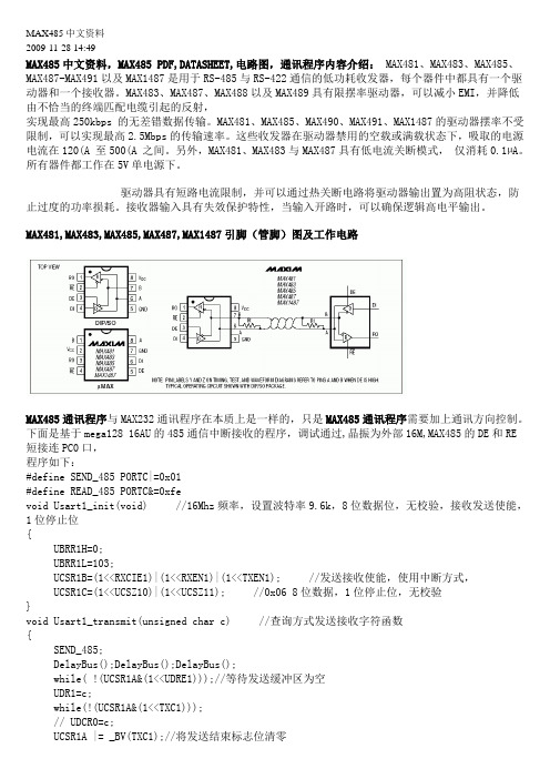
MAX481,MAX483,MAX485,MAX487,MAX1487引脚(管脚)图及工作电路MAX485通讯程序与MAX232通讯程序在本质上是一样的,只是MAX485通讯程序需要加上通讯方向控制。
下面是基于mega128 16AU的485通信中断接收的程序,调试通过,晶振为外部16M,MAX485的DE和RE短接连PC0口,程序如下:#define SEND_485 PORTC|=0x01#define READ_485 PORTC&=0xfevoid Usart1_init(void) //16Mhz频率,设置波特率9.6k,8位数据位,无校验,接收发送使能,1位停止位{UBRR1H=0;UBRR1L=103;UCSR1B=(1<<RXCIE1)|(1<<RXEN1)|(1<<TXEN1); //发送接收使能,使用中断方式,UCSR1C=(1<<UCSZ10)|(1<<UCSZ11); //0x06 8位数据,1位停止位,无校验}void Usart1_transmit(unsigned char c) //查询方式发送接收字符函数{SEND_485;DelayBus();DelayBus();DelayBus();while( !(UCSR1A&(1<<UDRE1)));//等待发送缓冲区为空UDR1=c;while(!(UCSR1A&(1<<TXC1)));// UDCR0=c;UCSR1A |= _BV(TXC1);//将发送结束标志位清零// SET_BIT(UCSR1A,);READ_485;direction++;}SIGNAL(SIG_UART1_RECV)//serial port 1 {if(UCSR1A&(1<<RXC1)){rec1buff=UDR1;rec1_flag=1;。
MAX491EESD+中文资料
Driver Input Voltage (DI).............................-0.5V to (VCC + 0.5V)
Driver Output Voltage (Y, Z; A, B) ..........................-8V to +12.5V
Receiver Input Voltage (A, B).................................-8V to +12.5V
元器件交易网
MAX481E/MAX483E/MAX485E/MAX487E–MAX491E/MAX1487E
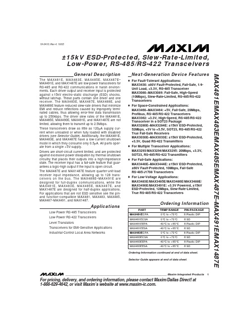
±15kV ESD-Protected, Slew-Rate-Limited, Low-Power, RS-485/RS-422 Transceivers
ABSOLUTE MAXIMUM RATINGS
General Description
The MAX481E, MAX483E, MAX485E, MAX487E– MAX491E, and MAX1487E are low-power transceivers for RS-485 and RS-422 communications in harsh environments. Each driver output and receiver input is protected against ±15kV electro-static discharge (ESD) shocks, without latchup. These parts contain one driver and one receiver. The MAX483E, MAX487E, MAX488E, and MAX489E feature reduced slew-rate drivers that minimize EMI and reduce reflections caused by improperly terminated cables, thus allowing error-free data transmission up to 250kbps. The driver slew rates of the MAX481E, MAX485E, MAX490E, MAX491E, and MAX1487E are not limited, allowing them to transmit up to 2.5Mbps.
MAX3490EESA+中文资料
General DescriptionDevices in the MAX3483E family (MAX3483E/MAX3485E/MAX3486E/MAX3488E/MAX3490E/MAX3491E) are ±15kV ESD-protected, +3.3V, low-power transceivers for RS-485 and RS-422 communications. Each device con-tains one driver and one receiver. The MAX3483E and MAX3488E feature slew-rate-limited drivers that minimize EMI and reduce reflections caused by improperly termi-nated cables, allowing error-free data transmission at data rates up to 250kbps. The partially slew-rate-limited MAX3486E transmits up to 2.5Mbps. The MAX3485E,MAX3490E, and MAX3491E transmit at up to 12Mbps.All devices feature enhanced electrostatic discharge (ESD) protection. All transmitter outputs and receiver inputs are protected to ±15kV using IEC 1000-4-2 Air-Gap Discharge, ±8kV using IEC 1000-4-2 Contact Discharge, and ±15kV using the Human Body Model.Drivers are short-circuit current limited and are protect-ed against excessive power dissipation by thermal shutdown circuitry that places the driver outputs into a high-impedance state. The receiver input has a fail-safe feature that guarantees a logic-high output if both inputs are open circuit.The MAX3488E, MAX3490E, and MAX3491E feature full-duplex communication, while the MAX3483E,MAX3485E, and MAX3486E are designed for half-duplex communication.ApplicationsTelecommunicationsIndustrial-Control Local Area Networks Transceivers for EMI-Sensitive Applications Integrated Services Digital Networks Packet SwitchingFeatureso ESD Protection for RS-485 I/O Pins±15kV—Human Body Model±8kV—IEC 1000-4-2, Contact Discharge ±15kV—IEC 1000-4-2, Air-Gap Discharge o Operate from a Single +3.3V Supply—No Charge Pump Required o Interoperable with +5V Logic o Guaranteed 12Mbps Data Rate (MAX3485E/MAX3490E/MAX3491E)o Slew-Rate Limited for Errorless Data Transmission (MAX3483E/MAX3488E) o 2nA Low-Current Shutdown Mode(MAX3483E/MAX3485E/MAX3486E/MAX3491E)o -7V to +12V Common-Mode Input Voltage Range o Full-Duplex and Half-Duplex Versions Available o Industry-Standard 75176 Pinout (MAX3483E/MAX3485E/MAX3486E)o Current-Limiting and Thermal Shutdown for Driver Overload ProtectionMAX3483E/MAX3485E/MAX3486E/MAX3488E/MAX3490E/MAX3491E3.3V-Powered, ±15kV ESD-Protected, 12Mbps and Slew-Rate-Limited T rue RS-485/RS-422 T ransceivers________________________________________________________________Maxim Integrated Products119-1474; Rev 0; 4/99Selector GuideOrdering InformationOrdering Information continued at end of data sheet.For free samples & the latest literature: , or phone 1-800-998-8800.For small orders, phone 1-800-835-8769.M A X 3483E /M A X 3485E /M A X 3486E /M A X 3488E /M A X 3490E /M A X 3491E3.3V-Powered, ±15kV ESD-Protected, 12Mbps and Slew-Rate-Limited T rue RS-485/RS-422 T ransceiversABSOLUTE MAXIMUM RATINGSDC ELECTRICAL CHARACTERISTICS(V = +3.3V ±0.3V, T = T to T , unless otherwise noted. Typical values are at T = +25°C.)Stresses beyond those listed under “Absolute Maximum Ratings” may cause permanent damage to the device. These are stress ratings only, and functional operation of the device at these or any other conditions beyond those indicated in the operational sections of the specifications is not implied. Exposure to absolute maximum rating conditions for extended periods may affect device reliability.Supply Voltage (V CC ).............................................................+7V Control Input Voltage (RE , DE).................................-0.3V to +7V Driver Input Voltage (DI)...........................................-0.3V to +7V Driver Output Voltage (A, B, Y, Z).......................-7.5V to +12.5V Receiver Input Voltage (A, B)..............................-7.5V to +12.5V Receiver Output Voltage (RO)....................-0.3V to (V CC + 0.3V)Continuous Power Dissipation (T A = +70°C)8-Pin SO (derate 5.88mW/°C above +70°C)..................471mW 8-Pin Plastic DIP (derate 9.09mW/°C above +70°C).....727mW14-Pin SO (derate 8.33mW/°C above +70°C)................667mW 14-Pin Plastic DIP (derate 10mW/°C above +70°C)......800mW Operating Temperature RangesMAX34_ _ EC_ _...................................................0°C to +70°C MAX34_ _ EE_ _.................................................-40°C to +85°C Storage Temperature Range.............................-65°C to +150°C Lead Temperature (soldering, 10sec).............................+300°CMAX3483E/MAX3485E/MAX3486E/MAX3488E/MAX3490E/MAX3491E3.3V-Powered, ±15kV ESD-Protected, 12Mbps and Slew-Rate-Limited T rue RS-485/RS-422 T ransceiversDC ELECTRICAL CHARACTERISTICS (continued)(V CC = +3.3V ±0.3V, T A = T MIN to T MAX , unless otherwise noted. Typical values are at T A = +25°C.)DRIVER SWITCHING CHARACTERISTICS—MAX3485E/MAX3490E/MAX3491E(V = +3.3V, T = +25°C.)DRIVER SWITCHING CHARACTERISTICS—MAX3486E(V = +3.3V, T = +25°C.)*MAX3488E and MAX3491E will be compliant to ±8kV per IEC 1000-4-2 Contact Discharge by September 1999.M A X 3483E /M A X 3485E /M A X 3486E /M A X 3488E /M A X 3490E /M A X 3491E3.3V-Powered, ±15kV ESD-Protected, 12Mbps and Slew-Rate-Limited T rue RS-485/RS-422 T ransceivers4_______________________________________________________________________________________DRIVER SWITCHING CHARACTERISTICS—MAX3483E/MAX3488E(V CC = +3.3V, T A = +25°C.)RECEIVER SWITCHING CHARACTERISTICS(V CC = +3.3V, T A = +25°C.)Note 1:∆V OD and ∆V OC are the changes in V OD and V OC , respectively, when the DI input changes state.Note 2:Measured on |t PLH (Y) - t PHL (Y)|and |t PLH (Z) - t PHL (Z)|.Note 3:The transceivers are put into shutdown by bringing RE high and DE low. If the inputs are in this state for less than 80ns, thedevices are guaranteed not to enter shutdown. If the inputs are in this state for at least 300ns, the devices are guaranteed to have entered shutdown. See Low-Power Shutdown Mode section.MAX3483E/MAX3485E/MAX3486E/MAX3488E/MAX3490E/MAX3491E3.3V-Powered, ±15kV ESD-Protected, 12Mbps and Slew-Rate-Limited T rue RS-485/RS-422 T ransceivers_______________________________________________________________________________________5Typical Operating Characteristics(V CC = +3.3V, T A = +25°C, unless otherwise noted.)252015105000.51.01.52.02.53.53.0OUTPUT CURRENT vs.RECEIVER OUTPUT LOW VOLTAGEM A X 3483E -01OUTPUT LOW VOLTAGE (V)O U T P U T C U R R E N T (m A )-20-18-16-14-12-10-8-6-4-2000.51.01.52.02.53.53.0OUTPUT CURRENT vs.RECEIVER OUTPUT HIGH VOLTAGEM A X 3483E -02OUTPUT HIGH VOLTAGE (V)O U T P U T C U R R E N T (m A )3.003.053.103.153.203.253.30-40-20020406010080RECEIVER OUTPUT HIGH VOLTAGEvs. TEMPERATURETEMPERATURE (°C)O U T P U T H I G H V O L T A G E (V )00.10.20.30.40.50.60.70.8-40-2020406010080RECEIVER OUTPUT LOW VOLTAGEvs. TEMPERATURETEMPERATURE (°C)O U T P U T L O W V O L T A G E (V )2505075100125150175024681012OUTPUT CURRENT vs.DRIVER OUTPUT LOW VOLTAGEM A X 3483E -07OUTPUT LOW VOLTAGE (V)O U T P U T C U R R E N T (m A )100908070605040302010000.5 1.0 1.5 2.0 2.5 3.53.0DRIVER OUTPUT CURRENT vs.DIFFERENTIAL OUTPUT VOLTAGEM A X 3483E -05DIFFERENTIAL OUTPUT VOLTAGE (V)O U T P U T C U R R E N T (m A )1.61.71.81.92.02.12.22.32.42.62.5-40-20020406010080DRIVER DIFFERENTIAL OUTPUT VOLTAGE vs. TEMPERATURETEMPERATURE (°C)D I F FE R E N T I A L O U T P U T V O L T A G E (V )-100-80-60-40-20543210-7-6-3-4-5-2-1OUTPUT CURRENT vs.DRIVER OUTPUT HIGH VOLTAGEM A X 3483E -08OUTPUT HIGH VOLTAGE (V)O U T P U T C U R R E N T (m A )M A X 3483E /M A X 3485E /M A X 3486E /M A X 3488E /M A X 3490E /M A X 3491E3.3V-Powered, ±15kV ESD-Protected, 12Mbps and Slew-Rate-Limited T rue RS-485/RS-422 T ransceivers0.80.70.91.01.11.2-40-2020406010080SUPPLY CURRENT vs. TEMPERATURETEMPERATURE (°C)S U P P L Y C U R R E N T (m A )Typical Operating Characteristics (continued)(V CC = +3.3V, T A = +25°C, unless otherwise noted.)0102030405060708010090-40-2020406010080SHUTDOWN CURRENT vs. TEMPERATUREM A X 3483E -10TEMPERATURE (°C)S H U T D O W N C U R R E N T (n A )Pin DescriptionMAX3483E/MAX3485E/MAX3486E/MAX3488E/MAX3490E/MAX3491E3.3V-Powered, ±15kV ESD-Protected, 12Mbps and Slew-Rate-Limited T rue RS-485/RS-422 T ransceivers_______________________________________________________________________________________7Figure 2. MAX3488E/MAX3490E Pin Configuration and Typical Operating CircuitFigure 3. MAX3491E Pin Configuration and Typical Operating CircuitFigure 1. MAX3483E/MAX3485E/MAX3486E Pin Configuration and Typical Operating CircuitM A X 3483E /M A X 3485E /M A X 3486E /M A X 3488E /M A X 3490E /M A X 3491E3.3V-Powered, ±15kV ESD-Protected, 12Mbps and Slew-Rate-Limited T rue RS-485/RS-422 T ransceivers8_______________________________________________________________________________________Figure 4. Driver V OD and V OC Figure 7. Driver Differential Output Delay and Transition TimesFigure 6. Receiver V OH and V OLFigure 5. Driver V OD with Varying Common-Mode VoltageMAX3483E/MAX3485E/MAX3486E/MAX3488E/MAX3490E/MAX3491E3.3V-Powered, ±15kV ESD-Protected, 12Mbps and Slew-Rate-Limited T rue RS-485/RS-422 T ransceivers_______________________________________________________________________________________9Figure 8. Driver Propagation TimesFigure 9. Driver Enable and Disable Times (t PZH , t PSH , t PHZ )Figure 10. Driver Enable and Disable Times (t PZL , t PSL , t PLZ )M A X 3483E /M A X 3485E /M A X 3486E /M A X 3488E /M A X 3490E /M A X 3491E3.3V-Powered, ±15kV ESD-Protected, 12Mbps and Slew-Rate-Limited T rue RS-485/RS-422 T ransceivers10______________________________________________________________________________________Figure 11. Receiver Propagation DelayFigure 12. Receiver Enable and Disable TimesNote 4: The input pulse is supplied by a generator with the following characteristics: f = 250kHz, 50% duty cycle, t r ≤6.0ns, Z O = 50Ω.Note 5: C L includes probe and stray capacitance._____________________Function TablesDevices with Receiver/Driver Enable(MAX3483E/MAX3485E/MAX3486E/MAX3491E)Table 1. Transmitting* B and A outputs are Z and Y, respectively, for full-duplex part (MAX3491E).X = Don’t care; High-Z = High impedanceTable 2. Receiving* DE is a “don’t care” (x) for the full-duplex part (MAX3491E).X = Don’t care; High-Z = High impedanceDevices without Receiver/Driver Enable(MAX3488E/MAX3490E)Table 3. TransmittingTable 4. Receiving___________Applications InformationThe MAX3483E/MAX3485E/MAX3486E/MAX3488E/MAX3490E/MAX3491E are low-power transceivers for RS-485 and RS-422 communications. The MAX3483E and MAX3488E can transmit and receive at data rates up to 250kbps, the MAX3486E at up to 2.5Mbps, and the MAX3485E/MAX3490E/MAX3491E at up to 12Mbps. The MAX3488E/MAX3490E/MAX3491E are full-duplex trans-ceivers, while the MAX3483E/MAX3485E/MAX3486E are half-duplex. Driver Enable (DE) and Receiver Enable (RE ) pins are included on the MAX3483E/MAX3485E/MAX3486E/MAX3491E. When disabled, the driver and receiver outputs are high impedance.Reduced EMI and Reflections (MAX3483E/MAX3486E/MAX3488E)The MAX3483E/MAX3488E are slew-rate limited, mini-mizing EMI and reducing reflections caused by improp-erly terminated cables. Figure 13 shows the driver output waveform of a MAX3485E/MAX3490E/MAX3491E transmitting a 125kHz signal, as well as the Fourier analysis of that waveform. High-frequency harmonics with large amplitudes are evident. Figure 14 shows the same information, but for the slew-rate-limited MAX3483E/MAX3488E transmitting the same signal. The high-frequency harmonics have much lower amplitudes,and the potential for EMI is significantly reduced.Low-Power Shutdown Mode(MAX3483E/MAX3485E/MAX3486E/MAX3491E)A low-power shutdown mode is initiated by bringing both RE high and DE low. The devices will not shut down unless both the driver and receiver are disabled (high impedance). In shutdown, the devices typically draw only 2nA of supply current.For these devices, the t PSH and t PSL enable times assume the part was in the low-power shutdown mode;the t PZH and t PZL enable times assume the receiver or driver was disabled, but the part was not shut down.MAX3483E/MAX3485E/MAX3486E/MAX3488E/MAX3490E/MAX3491E3.3V-Powered, ±15kV ESD-Protected, 12Mbps and Slew-Rate-Limited T rue RS-485/RS-422 T ransceivers______________________________________________________________________________________11INPUTS OUTPUT A, B RO ≥+0.2V 1≤-0.2V 0Inputs Open1INPUT OUTPUTS DI Z Y 101015MHz 500kHz/div 05MHz500kHz/div Figure 13. Driver Output Waveform and FFT Plot of MAX3485E/MAX3490E/MAX3491E Transmitting a 125kHz Signal Figure 14. Driver Output Waveform and FFT Plot of MAX3483E/ MAX3488E Transmitting a 125kHz SignalM A X 3483E /M A X 3485E /M A X 3486E /M A X 3488E /M A X 3490E /M A X 3491E3.3V-Powered, ±15kV ESD-Protected, 12Mbps and Slew-Rate-Limited T rue RS-485/RS-422 T ransceivers12______________________________________________________________________________________Figure 17. MAX3483E/MAX3488E Driver Propagation Delay Figure 19. MAX3483E/MAX3488E System Differential Voltage at 125kHz Driving 4000 Feet of Cable Figure 20. MAX3485E/MAX3490E/MAX3491E System Differential Voltage at 125kHz Driving 4000 Feet of CableDriver-Output Protection Excessive output current and power dissipation caused by faults or by bus contention are prevented by two mechanisms. A foldback current limit on the output stage provides immediate protection against short circuits over the whole common-mode voltage range (see Typical Operating Characteristics). In addition, a thermal shut-down circuit forces the driver outputs into a high-imped-ance state if the die temperature rises excessively.Propagation Delay Figures 15–18 show the typical propagation delays. Skew time is simply the difference between the low-to-high and high-to-low propagation delay. Small driver/receiver skew times help maintain a symmetrical mark-space ratio (50% duty cycle).The receiver skew time, |t PRLH- t PRHL|, is under 10ns (20ns for the MAX3483E/MAX3488E). The driver skew times are 8ns for the MAX3485E/MAX3490E/MAX3491E, 12ns for the MAX3486E, and typically under 50ns for the MAX3483E/MAX3488E.Line Length vs. Data Rate The RS-485/RS-422 standard covers line lengths up to 4000 feet. For line lengths greater than 4000 feet, see Figure 21 for an example of a line repeater.Figures 19 and 20 show the system differential voltage for parts driving 4000 feet of 26AWG twisted-pair wire at 125kHz into 120Ωloads.For faster data rate transmission, please consult the fac-tory.±15kV ESD Protection As with all Maxim devices, ESD-protection structures are incorporated on all pins to protect against electrostatic discharges encountered during handling and assembly. The driver outputs and receiver inputs of the MAX3483E family of devices have extra protection against static electricity. Maxim’s engineers have developed state-of-the-art structures to protect these pins against ESD of ±15kV without damage. The ESD structures withstand high ESD in all states: normal operation, shutdown, and powered down. After an ESD event, Maxim’s E versions keep working without latchup or damage.ESD protection can be tested in various ways; the transmitter outputs and receiver inputs of this product family are characterized for protection to the following limits:1)±15kV using the Human Body Model2)±8kV using the Contact-Discharge method specifiedin IEC 1000-4-23)±15kV using IEC 1000-4-2’s Air-Gap method.ESD Test Conditions ESD performance depends on a variety of conditions. Contact Maxim for a reliability report that documents test setup, test methodology, and test results.Human Body Model Figure 22a shows the Human Body Model and Figure 22b shows the current waveform it generates when dis-charged into a low impedance. This model consists of a 100pF capacitor charged to the ESD voltage of inter-est, which is then discharged into the test device through a 1.5kΩresistor.IEC 1000-4-2 The IEC 1000-4-2 standard covers ESD testing and performance of finished equipment; it does not specifi-cally refer to integrated circuits. The MAX3483E family of devices helps you design equipment that meets Level 4 (the highest level) of IEC 1000-4-2, without the need for additional ESD-protection components.The major difference between tests done using the Human Body Model and IEC 1000-4-2 is higher peak current in IEC 1000-4-2, because series resistance is lower in the IEC 1000-4-2 model. Hence, the ESD with-stand voltage measured to IEC 1000-4-2 is generally lower than that measured using the Human Body Model. Figure 23a shows the IEC 1000-4-2 model, and Figure 23b shows the current waveform for the ±8kV IEC 1000-4-2, Level 4 ESD contact-discharge test.Figure 21. Line Repeater for MAX3488E/MAX3490E/MAX3491EMAX3483E/MAX3485E/MAX3486E/MAX3488E/MAX3490E/MAX3491E3.3V-Powered, ±15kV ESD-Protected, 12Mbps and Slew-Rate-Limited T rue RS-485/RS-422 T ransceivers ______________________________________________________________________________________13M A X 3483E /M A X 3485E /M A X 3486E /M A X 3488E /M A X 3490E /M A X 3491EThe air-gap test involves approaching the device with a charged probe. The contact-discharge method connects the probe to the device before the probe is energized.Machine ModelThe Machine Model for ESD tests all pins using a 200pF storage capacitor and zero discharge resis-tance. Its objective is to emulate the stress caused when I/O pins are contacted by handling equipment during test and assembly. Of course, all pins require this protection, not just RS-485 inputs and outputs.Typical ApplicationsThe MAX3483E/MAX3485E/MAX3486E/MAX3488E/MAX3490E/MAX3491E transceivers are designed for bidirectional data communications on multipoint bus transmission lines. Figures 24 and 25 show typical net-work applications circuits. These parts can also be used as line repeaters, with cable lengths longer than 4000 feet, as shown in Figure 21.To minimize reflections, the line should be terminated at both ends in its characteristic impedance, and stub lengths off the main line should be kept as short as possible. The slew-rate-limited MAX3483E/MAX3488E and the partially slew-rate-limited MAX3486E are more tolerant of imperfect termination.3.3V-Powered, ±15kV ESD-Protected, 12Mbps and Slew-Rate-Limited T rue RS-485/RS-422 T ransceivers14______________________________________________________________________________________Figure 22a. Human Body ESD Test ModelFigure 22b. Human Body Current WaveformFigure 23a. IEC 1000-4-2 ESD Test ModelFigure 23b. IEC 1000-4-2 ESD Generator Current WaveformMAX3483E/MAX3485E/MAX3486E/MAX3488E/MAX3490E/MAX3491E3.3V-Powered, ±15kV ESD-Protected, 12Mbps and Slew-Rate-Limited T rue RS-485/RS-422 T ransceivers______________________________________________________________________________________15Figure 25. MAX3488E/MAX3490E/MAX3491E Full-Duplex RS-485 NetworkFigure 24. MAX3483E/MAX3485E/MAX3486E Typical RS-485 NetworkM A X 3483E /M A X 3485E /M A X 3486E /M A X 3488E /M A X 3490E /M A X 3491E3.3V-Powered, ±15kV ESD-Protected, 12Mbps and Slew-Rate-Limited T rue RS-485/RS-422 T ransceiversTRANSISTOR COUNT: 761Chip InformationOrdering Information (continued)Maxim cannot assume responsibility for use of any circuitry other than circuitry entirely embodied in a Maxim product. No circuit patent licenses are implied. Maxim reserves the right to change the circuitry and specifications without notice at any time.16____________________Maxim Integrated Products, 120 San Gabriel Drive, Sunnyvale, CA 94086 408-737-7600©1999 Maxim Integrated ProductsPrinted USAis a registered trademark of Maxim Integrated Products.。
MAX3232ECPE中文资料
MAX3222EEPN -40°C to +85°C 18 Plastic DIP —
MAX3232ECAE 0°C to +70°C 16 SSOP
—
MAX3232ECWE 0°C to +70°C 16 Wide SO —
MAX3232ECPE 0°C to +70°C 16 Plastic DIP —
Next-Generation Device Features
♦ For Space-Constrained Applications MAX3228E/MAX3229E: ±15kV ESD-Protected, +2.5V to +5.5V, RS-232 Transceivers in UCSP
*Dice are tested at TA = +25°C, DC parameters only. **EP = Exposed paddle.
Ordering Information continued at end of data sheet.
Pin Configurations, Selector Guide, and Typical Operating Circuits appear at end of data sheet.
MAX3222EETP
20 Thin QFN-40°C to +85°C EP** (5mm x
5mm)
T2055-5
MAX3222EEUP -40°C to +85°C 20 TSSOP
—
MAX3222EEAP -40°C to +85°C 20 SSOP
—
MAX3222EEWN -40°C to +85°C 18 Wide SO —
MAX485EEPA+中文资料

14-Pin Plastic DIP (derate 10.00mW/°C above +70°C) ..800mW 8-Pin SO (derate 5.88mW/°C above +70°C).................471mW 14-Pin SO (derate 8.33mW/°C above +70°C)...............667mW Operating Temperature Ranges MAX4_ _C_ _/MAX1487EC_ A .............................0°C to +70°C MAX4_ _E_ _/MAX1487EE_ A...........................-40°C to +85°C StorageБайду номын сангаасTemperature Range .............................-65°C to +160°C Lead Temperature (soldering, 10sec) .............................+300°C
Receiver Output Voltage (RO)....................-0.5V to (VCC + 0.5V)
Continuous Power Dissipation (TA = +70°C)
8-Pin Plastic DIP (derate 9.09mW/°C above +70°C) ....727mW
Ordering Information
PART MAX481ECPA MAX481ECSA MAX481EEPA MAX481EESA MAX483ECPA MAX483ECSA MAX483EEPA MAX483EESA
- 1、下载文档前请自行甄别文档内容的完整性,平台不提供额外的编辑、内容补充、找答案等附加服务。
- 2、"仅部分预览"的文档,不可在线预览部分如存在完整性等问题,可反馈申请退款(可完整预览的文档不适用该条件!)。
- 3、如文档侵犯您的权益,请联系客服反馈,我们会尽快为您处理(人工客服工作时间:9:00-18:30)。
________________________Applications
Low-Power RS-485 Transceivers Low-Power RS-422 Transceivers Level Translators Transceivers for EMI-Sensitive Applications Industrial-Control Local Area Networks
元器件交易网
±15kV ESD-Protected, Slew-Rate-Limited, Low-Power, RS-485/RS-422 Transceivers
MAX481E/MAX483E/MAX485E/MAX487E–MAX491E/MAX1487E
ABSOLUTE MAXIMUM RATINGS
____________________________Features
o ESD Protection: ±15kV—Human Body Model o Slew-Rate Limited for Error-Free Data Transmission (MAX483E/487E/488E/489E) o Low escent Current: 120µA (MAX483E/487E/488E/489E) 230µA (MAX1487E) 300µA (MAX481E/485E/490E/491E) o -7V to +12V Common-Mode Input Voltage Range o Three-State Outputs o 30ns Propagation Delays, 5ns Skew (MAX481E/485E/490E/491E/1487E) o Full-Duplex and Half-Duplex Versions Available o Allows up to 128 Transceivers on the Bus (MAX487E/MAX1487E) o Current Limiting and Thermal Shutdown for Driver Overload Protection
元器件交易网
19-0410; Rev 3; 7/96
±15kV ESD-Protected, Slew-Rate-Limited, Low-Power, RS-485/RS-422 Transceivers
_______________General Description
The MAX481E, MAX483E, MAX485E, MAX487E–MAX491E, and MAX1487E are low-power transceivers for RS-485 and RS-422 communications in harsh environments. Each driver output and receiver input is protected against ±15kV electrostatic discharge (ESD) shocks, without latchup. These parts contain one driver and one receiver. The MAX483E, MAX487E, MAX488E, and MAX489E feature reduced slewrate drivers that minimize EMI and reduce reflections caused by improperly terminated cables, thus allowing error-free data transmission up to 250kbps. The driver slew rates of the MAX481E, MAX485E, MAX490E, MAX491E, and MAX1487E are not limited, allowing them to transmit up to 2.5Mbps. These transceivers draw as little as 120µA supply current when unloaded or when fully loaded with disabled drivers (see Selection Table ). Additionally, the MAX481E, MAX483E, and MAX487E have a low-current shutdown mode in which they consume only 0.5µA. All parts operate from a single +5V supply. Drivers are short-circuit current limited, and are protected against excessive power dissipation by thermal shutdown circuitry that places their outputs into a high-impedance state. The receiver input has a fail-safe feature that guarantees a logic-high output if the input is open circuit. The MAX487E and MAX1487E feature quarter-unit-load receiver input impedance, allowing up to 128 transceivers on the bus. The MAX488E–MAX491E are designed for fullduplex communications, while the MAX481E, MAX483E, MAX485E, MAX487E, and MAX1487E are designed for halfduplex applications. For applications that are not ESD sensitive see the pin- and function-compatible MAX481, MAX483, MAX485, MAX487–MAX491, and MAX1487.
________________________________________________________________ Maxim Integrated Products
1
For free samples & the latest literature: , or phone 1-800-998-8800
MAX481E/MAX483E/MAX485E/MAX487E–MAX491E/MAX1487E
______________Ordering Information
PART MAX481ECPA MAX481ECSA MAX481EEPA MAX481EESA TEMP. RANGE 0°C to +70°C 0°C to +70°C -40°C to +85°C -40°C to +85°C PIN-PACKAGE 8 Plastic DIP 8 SO 8 Plastic DIP 8 SO
Stresses beyond those listed under “Absolute Maximum Ratings” may cause permanent damage to the device. These are stress ratings only, and functional operation of the device at these or any other conditions beyond those indicated in the operational sections of the specifications is not implied. Exposure to absolute maximum rating conditions for extended periods may affect device reliability.
Ordering Information continued on last page.
______________________________________________________________Selection Table
PART NUMBER MAX481E MAX483E MAX485E MAX487E MAX488E MAX489E MAX490E MAX491E MAX1487E HALF/FULL DUPLEX Half Half Half Half Full Full Full Full Half DATA RATE (Mbps) 2.5 0.25 2.5 0.25 0.25 0.25 2.5 2.5 2.5 SLEW-RATE LIMITED No Yes No Yes Yes Yes No No No LOW-POWER SHUTDOWN Yes Yes No Yes No No No No No RECEIVER/ DRIVER ENABLE Yes Yes Yes Yes No Yes No Yes Yes QUIESCENT CURRENT (µA) 300 120 300 120 120 120 300 300 230 NUMBER OF TRANSMITTERS ON BUS 32 32 32 128 32 32 32 32 128 PIN COUNT 8 8 8 8 8 14 8 14 8
Supply Voltage (VCC) .............................................................12V – — – Control Input Voltage (RE , DE)...................-0.5V to (VCC + 0.5V) Driver Input Voltage (DI).............................-0.5V to (VCC + 0.5V) Driver Output Voltage (Y, Z; A, B) ..........................-8V to +12.5V Receiver Input Voltage (A, B).................................-8V to +12.5V Receiver Output Voltage (RO)....................-0.5V to (VCC + 0.5V) Continuous Power Dissipation (TA = +70°C) 8-Pin Plastic DIP (derate 9.09mW/°C above +70°C) ....727mW 14-Pin Plastic DIP (derate 10.00mW/°C above +70°C) ..800mW 8-Pin SO (derate 5.88mW/°C above +70°C).................471mW 14-Pin SO (derate 8.33mW/°C above +70°C)...............667mW Operating Temperature Ranges MAX4_ _C_ _/MAX1487EC_ A .............................0°C to +70°C MAX4_ _E_ _/MAX1487EE_ A...........................-40°C to +85°C Storage Temperature Range .............................-65°C to +160°C Lead Temperature (soldering, 10sec) .............................+300°C