22AC2-UL;中文规格书,Datasheet资料
DV2002TL2;DV2002L2;中文规格书,Datasheet资料
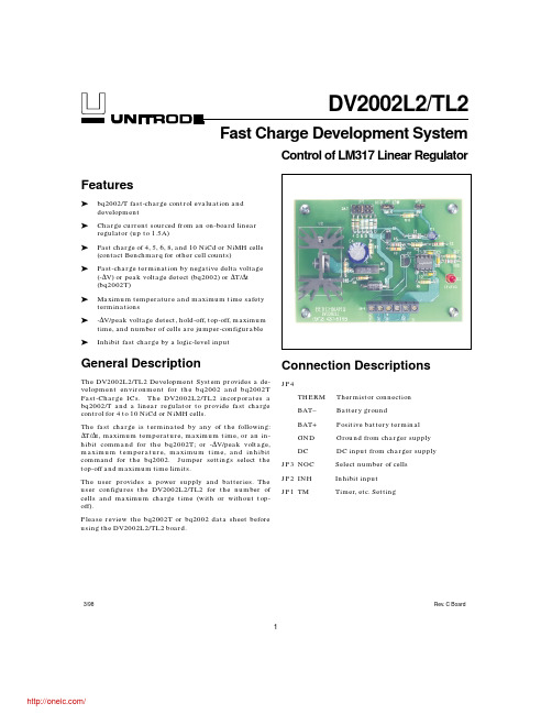
Featuresäbq2002/T fast-charge control evaluation and developmentäCharge current sourced from an on-board linear regulator (up to 1.5A)äFast charge of 4,5,6,8,and 10NiCd or NiMH cells (contact Benchmarq for other cell counts)äFast-charge termination by negative delta voltage (-∆V) or peak voltage detect (bq2002) or ∆T/∆t (bq2002T)äMaximum temperature and maximum time safety terminationsä-∆V/peak voltage detect,hold-off,top-off,maximum time,and number of cells are jumper-configurable äInhibit fast charge by a logic-level inputGeneral DescriptionThe DV2002L2/TL2Development System provides a de-velopment environment for the bq2002and bq2002T Fast-Charge ICs.The DV2002L2/TL2incorporates a bq2002/T and a linear regulator to provide fast charge control for 4to 10NiCd or NiMH cells.The fast charge is terminated by any of the following:∆T/∆t,maximum temperature,maximum time,or an in-hibit command for the bq2002T;or -∆V/peak voltage,maximum temperature,maximum time,and inhibit command for the bq2002.Jumper settings select the top-off and maximum time limits.The user provides a power supply and batteries.The user configures the DV2002L2/TL2for the number of cells and maximum charge time (with or without top-off).Please review the bq2002T or bq2002data sheet before using the DV2002L2/TL2board.Connection DescriptionsJP4THERM Thermistor connection BAT–Battery groundBAT+Positive battery terminal GND Ground from charger supply DC DC input from charger supply JP3NOC Select number of cells JP2INH Inhibit input JP1TMTimer,etc.Setting1DV2002L2/TL23/98Rev.C BoardFast Charge Development SystemControl of LM317LinearRegulatorFixed ConfigurationThe DV2002L2/TL2board has the following fixed char-acteristics:V CC(4.75–5.25V)is regulated on-board from the supply at connector JP4(DC:GND).LED indicates charge status.Charge initiates on the later application of the battery or DC,which provides V CC to the bq2002/T.As shipped from Benchmarq,the DV2002L2/TL2linear regulator is configured to a charging current of1.25A. This current level is controlled by the value of sense re-sistor R7by the relationship:I=1.25V RCHG7The value of R7at shipment is1Ω.This resistor can be changed depending on the application.The suggested maximum I CHG for the DV2002L2/TL2 board is1.5A.U2must be mounted to an appropri-ate heat sink.The maximum cell voltage(MCV)is scaled to2V/cell. With the provided NTC thermistor connected between THERM and BAT–,TCO=50°C.The thermistor is identified by the serial number suffix as follows:Jumper-Selectable Configuration The DV2002L2/TL2must be configured as described be-low.INH(JP2):Enables/disables charge inhibit(see bq2002/T data sheet).TM(JP1):Selects fast charge safety time/top-off(see bq2002/T data sheet).Number of Cells(JP3):A resistor-divider network is provided to select4to10cells(the resulting resistor value equals N–1cells).RB1is a100KΩresistor,and RB2(RB20–RB25)is jumper-selected.Temperature Disable:Connecting a10KΩresistor be-tween THERM and BAT–disables temperature control. Setup Procedure1.Configure TM,INH,and number-of-cells(NOC)jumpers.2.Connect the provided thermistor or a10KΩresistorbetween THERM and BAT–.3.Attach the battery pack to BAT+and BAT–.Fortemperature control,the thermistor must contactthe cells.4.Attach DC current source to DC(+)and GND(–)connections in JP4.2DV2002L2/TL2Rev.C Board Jumper Setting Pin State [ 1 2 ] 3Disabled (high)1 [23 ]Enabled (low)Jumper Setting Pin State [ 1 2 ] 3High1 [23 ]Low1 2 3FloatClosed Jumper Number of Cells R1310R128R116R105R94InputVoltage Current Resistance Wattage to 25V1A 1.25Ω2W1.5A0.83Ω2W Table 1. Lookup Table for R7 SelectionIdentifier ThermistorK1Keystone RL0703-5744-103-S1 (blank)Philips 2322-640-63103F1Fenwal Type 16,197-103LA6-A01 O1Ozhumi 150-108-00(4)S1Semetic 103AT-23DV2002L2/TL2Rev.C BoardSymbol DescriptionMinimumTypicalMaximumUnit I DC Maximum input current -- 1.5A V DC Maximum input voltage 4.0+V BAT or 10-18 + V BAT or 25V V BAT BAT input voltage --24V V THTHERM input voltage0.5-5VDV2002L2/TL2 Board Schematic* For the DV2002L2, U1 is the bq2002, R5 is 3.57 k , and R18 is open.W ***IMPORTANT NOTICETexas Instruments and its subsidiaries (TI) reserve the right to make changes to their products or to discontinue any product or service without notice, and advise customers to obtain the latest version of relevant information to verify, before placing orders, that information being relied on is current and complete. All products are sold subject to the terms and conditions of sale supplied at the time of order acknowledgement, including those pertaining to warranty, patent infringement, and limitation of liability.TI warrants performance of its semiconductor products to the specifications applicable at the time of sale in accordance with TI’s standard warranty. Testing and other quality control techniques are utilized to the extent TI deems necessary to support this warranty. Specific testing of all parameters of each device is not necessarily performed, except those mandated by government requirements.CERTAIN APPLICATIONS USING SEMICONDUCTOR PRODUCTS MAY INVOLVE POTENTIAL RISKS OF DEATH, PERSONAL INJURY, OR SEVERE PROPERTY OR ENVIRONMENTAL DAMAGE (“CRITICAL APPLICATIONS”). TI SEMICONDUCTOR PRODUCTS ARE NOT DESIGNED, AUTHORIZED, OR WARRANTED TO BE SUITABLE FOR USE IN LIFE-SUPPORT DEVICES OR SYSTEMS OR OTHER CRITICAL APPLICATIONS. INCLUSION OF TI PRODUCTS IN SUCH APPLICATIONS IS UNDERSTOOD TO BE FULLY AT THE CUSTOMER’S RISK.In order to minimize risks associated with the customer’s applications, adequate design and operating safeguards must be provided by the customer to minimize inherent or procedural hazards.TI assumes no liability for applications assistance or customer product design. TI does not warrant or represent that any license, either express or implied, is granted under any patent right, copyright, mask work right, or other intellectual property right of TI covering or relating to any combination, machine, or process in which such semiconductor products or services might be or are used. TI’s publication of information regarding any third party’s products or services does not constitute TI’s approval, warranty or endorsement thereof.Copyright © 1999, Texas Instruments Incorporated分销商库存信息:TIDV2002TL2DV2002L2。
EETUQ2A272KJ中文资料(panasonic)中文数据手册「EasyDatasheet - 矽搜」

00 Nov. 2012
芯片中文手册,看全文,戳
铝电解电容器/ UQ
■ 标准产品
耐力:85°C 2000ħ
机箱尺寸
W.V.
Cap.
(120赫兹) Dia.
长度
(±20 %)
型号
PET套
码头长度
4.0 mm
(无顶板)
规范
最小包装台数
波纹
tan δ
当前
(120赫兹)
(120赫兹) (+20 °C)
■ 纹波电流频率修正系数
额定电压
16 V.DC to 100 V.DC /C.F. 160 V.DC to 450 V.DC /C.F.
频率(Hz)
50
60
100
120
500
1k
10 k可
0.93
0.95
0.99
1.00
1.05
1.08
1.15
0.75
0.80
0.95
1.00
1.20
1.25
1.40
0.8
4.0±0.5 2.0 max. Terminal
(t=0.8)
(3.5)
1.5±0.2
Top of spin
Standard terminal type doesnot require terminal trimming process.
Design and specifications are each subject to change without notice. Ask factory for the current technical specifications before purchase and/or use. Should a safety concern arise regarding this product, please be sure to contact us immediately.
QS5K2TR;中文规格书,Datasheet资料
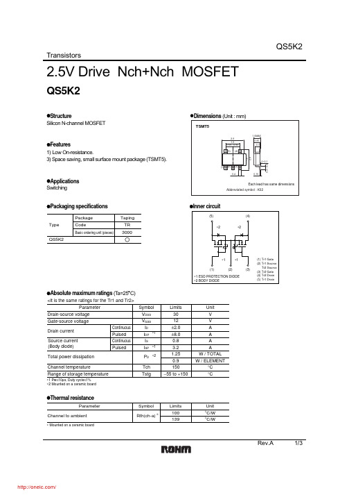
TransistorsRev.A 1/32.5V Drive Nch+Nch MOSFETQS5K2z Structure z Dimensions (Unit : mm) Silicon N-channel MOSFETz Features1) Low On-resistance.3) Space saving, small surface mount package (TSMT5).zSwitchingz Packaging specifications z Inner circuitz Absolute maximum ratings (T a=25°C)∗1∗2∗1ParameterV V DSS Symbol V V GSS A I DA I DP A I SAI SP W / TOTAL P D °C Tch °CTstgLimits Unit Drain-source voltage Gate-source voltage Drain current Total power dissipation Channel temperatureRange of storage temperatureContinuous Pulsed Continuous Pulsed∗1 Pw ≤10µs, Duty cycle ≤1%∗2 Mounted on a ceramic boardSource current (Body diode)30150−55 to +15012±2.0±8.00.83.21.25W / ELEMENT0.9<It is the same ratings for the Tr1 and Tr2>z Thermal resistanceParameter°C/W Rth(ch-a)Symbol Limits Unit Channel to ambient100°C/W139∗ Mounted on a ceramic board∗TransistorsRev.A 2/3z Electrical characteristics (T a=25°C)z Body diode characteristics (Source-drain) (T a=25°C)V SD −−1.2VI S = 3.2A, V GS =0VForward voltage∗ PulsedParameter Symbol Min.Typ.Max.UnitConditions∗<It is the same characteristics for the Tr1 and Tr2>TransistorsRev.A 3/3DRAIN-SOURCE VOLTAGE : V DS (V)101001000C A P A C I T A N C E : C (p F )Fig.1 Typical Capacitancevs. Drain-Source VoltageGATE-SOURCE VOLTAGE : V GS (V)0.0010.010.1110D R A I N C U R RE N T : I D (A )Fig.4 Typical Transfer CharacteristicsSOURCE-DRAIN VOLTAGE : V SD(V)S O U R C E C U R R E N T : I S (A )Fig.6 Source Current vs. Source-Drain VoltageGATE-SOURCE VOLTAGE : V GS (V)100200300S T A T I C D R A I N -S O U R C E O N -S T A T E R E S I S TA N C E : R D S (m Ω)Fig.5 Static Drain-SourceOn-State Resistance vs.Gate source Voltagez Electrical characteristics curvesDRAIN CURRENT : I D (A)1101001000S W I T C H I N G T I M E : t (n s )Fig.2 Switching CharacteristicsTOTAL GATE CHARGE : Qg (nC)123456G A T E -S O U R C E V O L T A G E : V G S (V )Fig.3 Dynamic Input CharacteristicsDRAIN CURRENT : I D (A)S T A T I C D R A I N -S O U R C E O N -S T A T E R E S I S T A N C E : R D S (o n ) (m Ω)Fig.7 Static Drain-Source On-State Resistance vs. Drain Current ( Ι )DRAIN CURRENT : I D (A)S T A T I C D R A I N -S O U R C E O N -S T A T E R E S I S T A N C E : R D S (o n ) (m Ω)Fig.8 Static Drain-Source On-State Resistance vs. Drain Current ( ΙΙ )DRAIN CURRENT : I D (A)S T A T I C D R A I N -S O U R C E O N -S T A T E R E S I S T A N C E : R D S (o n ) (m Ω)Fig.9 Static Drain-Source On-State Resistance vs. Drain Current ( ΙΙΙ )AppendixAbout Export Control Order in JapanProducts described herein are the objects of controlled goods in Annex 1 (Item 16) of Export T rade ControlOrder in Japan.In case of export from Japan, please confirm if it applies to "objective" criteria or an "informed" (by MITI clause)on the basis of "catch all controls for Non-Proliferation of Weapons of Mass Destruction.Appendix1-Rev1.1分销商库存信息: ROHMQS5K2TR。
电源22-29V 0.6A恒流 规格书1

规格书SPECIFICATION FOR APPROVAL 客户名称(CUSTOMER):客户料号(PART NO.):客户品名(DESCRIPTION):品名(DESCRIPTION):22-29V0.6A日期(DATE):2012-02-16承认签章后请回传Please return to us one copy of“SPECIFICATION FOR APPROVAL”with your approved signatures承认书APPROVED SIGNATURES客户承认(CUSTOMER APPROVAL)公司承认(APPROVAL)工程师ENGINEER审核CHECKEDBY批准APPROVAL BY工程师ENGINEER审核CHECKEDBY批准APPROVALBY盖章签署(CHOP&SIGNATU RES)盖章签署(CHOP&SIGNATU RES)日期(DATE)日期(DATE)目录变更履历表 (3)1.导言Introduction (4)1.1电源概况Power Supply Overview (4)1.2支持文件Applicable Documents (4)2电气规格Electrical Specification (5)2.1AC输入AC Input (5)2.1.1输入电压Input Voltage (5)2.1.2输入频率Input Frequency (5)2.1.3冲击电流Inrush Current (5)2.1.4最大输入电流Input Current Limiting (5)2.1.5效率Efficiency (5)2.1.6功率因数Power factor (5)2.2输出规格Output Specification (5)2.2.1电压调整率DC Voltage Regulation (5)2.2.2输出电流DC Output Current (6)2.2.3输出纹波与噪声Output Ripple and Noise (6)2.2.4输出动态负载响应定电流模式Output Dynamic Load Response CC model (6)2.2.5电压过冲Overshoot at turn-on/turn-off (6)2.3保护功能Protection Function (7)2.3.1短路保护Short Circuit Protection (7)2.3.2过流保护Over Current Protection (7)2.4时序特性Timing (7)2.4.1保持时间Hold up Time (7)2.4.2启动时间Start up Time (7)3.环境要求Environment Requirement (7)3.1温度Temperature (7)3.2湿度Humidity (7)3.3海拔高度Altitude (7)4.可靠性Reliability (8)4.1平均无故障间隔时间MTBF(MIL-HDBK-217F) (8)4.2老化寿命测试Burn-in and Life test (8)5.产品安规要求Product Safety Requirement (8)5.1标准Standard (8)5.2泄露电流Leakage Current (8)5.3绝缘阻抗Insulation Resistance (8)5.4绝缘强度Dielectric Strength Testing (8)6.结构尺寸Mechanical Dimensions(单位:mm Unit:mm) (8)6.1标贴Label (8)6.2结构尺寸Mechanical Dimensions (9)7声明Statement (9)变更履历表Revision History承认书版本Spec.Edition发行日期Release Date修改内容Modified content产品版本Product EditionRev:A002012-02-16初版Initial1.1电源概况Power Supply Overview本产品效率高,可靠性高等特点,具有短路保护,过流保护等保护功能。
LTC6802IG-2#PBF;LTC6802IG-2#TRPBF;中文规格书,Datasheet资料

Pin Configuration
V+ 1 C12 2 S12 3 C11 4 S11 5 C10 6 S10 7 C9 8 S9 9 C8 10 S8 11 C7 12 S7 13 C6 14 S6 15 C5 16 S5 17 C4 18 S4 19 C3 20 S3 21 C2 22
TOP VIEW
Typical Application
NEXT 12-CELL PACK ABOVE
+
12-CELL BATTERY
STRING +
+
NEXT 12-CELL PACK BELOW
V+
LTC6802-2
DIE TEMP
REGISTERS AND
CONTROL
MUX
SERIAL DATA
4-BIT ADDRESS
Many LTC6802-2 devices can be stacked to measure the voltage of each cell in a long battery string. Each LTC6802-2 has an individually addressable serial interface, allowing up to 16 LTC6802-2 devices to interface to one control processor and operate simultaneously.
Multicell Addressable Battery Stack Monitor
Description
The LTC®6802-2 is a complete battery monitoring IC that includes a 12-bit ADC, a precision voltage reference, a high voltage input multiplexer and a serial interface. Each LTC6802-2 can measure 12 series connected battery cells, with a total input voltage up to 60V. The voltage on all 12 input channels can be measured within 13ms.
2SC2258中文资料

Collector current IC (A)
Base-emitter voltage VBE (V)
hFE IC
240
VCE=10V
fT I E
Collector output capacitance C (pF) (Common base, input open circuited) ob
Base-emitter voltage VBE (V)
IC I B
Collector-emitter saturation voltage VCE(sat) (V)
120
VCE=10V TC=25˚C
VCE(sat) IC
100
IC/IB=10
IB VBE
3.0
VCE=10V TC=25˚C
*2
Unit V V V mA mA W °C °C
1 2 0.75±0.1 4.6±0.2 0.5±0.1 0.5±0.1 2.3±0.2 3 1.76±0.1
150 −55 to +150
Note) *1: Without heat sink *2 :With a 100 × 100 × 2 mm Al heat sink
80
Collector current IC (mA)
80
3
60
60
2
(2)
40
0.2mA
40
1
20
20
0
0
0 40 80 120 160
0
2
4
6
8
10
0
0
0.4
0.8
1.2
1.6
2.0
Ambient temperature Ta (°C)
2SC5712(TE12L,F);中文规格书,Datasheet资料
♦: Single nonrepetitive pulse
Ta = 25°C 0.1 Note that the curves for 100 ms*,
10 s* and DC operation* will be
different when the devices aren’t
mounted on an FR4 board (glass
Unit: mm
• High DC current gain: hFE = 400 to 1000 (IC = 0.3 A) • Low collector-emitter saturation voltage: VCE (sat) = 0.14 V (max) • High-speed switching: tf = 120 ns (typ.)
Note 2: Using continuously under heavy loads (e.g. the application of high temperature/current/voltage and the significant change in temperature, etc.) may cause this product to decrease in the reliability significantly even if the operating conditions (i.e. operating temperature/current/voltage, etc.) are within the absolute maximum ratings. Please design the appropriate reliability upon reviewing the Toshiba Semiconductor Reliability Handbook (“Handling Precautions”/“Derating Concept and Methods”) and individual reliability data (i.e. reliability test report and estimated failure rate, etc).
250V22000uF电容的铝电解电容器
发布日期:2011年6月25日Issued date:DOC12,2011客户名称:Customer:产品规格书Products specification产品种类:铝电解电容器Products types:Aluminum Electrolytic Capacitors产品代码:UGF5AProducts code sigh:产品规格:250V22000μFφ90×170Specification深圳市雅达康电子科技有限公司YDK Technology Ltd.,Shenzhen拟制Designed审核Checked批准Approved刘小姐朱建平一、适用范围Adapt range本产品规格书适用于深圳市雅达康电子科技有限公司250V22000μF铝电解电容器产品。
The products specification is adapted to 250V22000μF Aluminum Electrolytic Capacitors ofYDK Technology Ltd.,Shenzhen二、技术性能Specifications项目Item 特性Performance characteristics使用温度范围(℃)Operation temperature range-40~+105额定电压(V)Rated voltage 250浪涌电压(V)Surge voltage 300标称电容量(μF)Nominal capacitance 22000标称电容量允许偏差(%)Capacitance tolerance±20%漏电流(mA)Leakage current(at 20℃,afer 5minutes)5损耗角正切值(tg δ)Dissipation factor (20℃,120Hz)0.25Ripple current (105℃120Hz)(Arms)56耐久性(105℃)Load life5000小时5000hours三、外形图及尺寸表Case size table(mm )四、纹波电流修正系数ripple current multipliers:频率修正系数Frequency Coefficient 温度修正系数Temperature coefficientφD ±0.7889L ±1.57170F ±0.4131.75频率Freq (Hz)50\601203001K ≥10K 系数factor0.81.001.101.301.40五、试验方法及要求Tests项目Item试验条件Test conditions性能要求Requirements浪涌电压Surge voltage 温度+15~+35℃,施加规定的浪涌电压,充电30秒,放电5分30秒,共循环1000次。