JPAD5-200中文资料
VN800S资料

(*) See note at page 7Rev. 1Switching time WaveformsFigure 3: WaveformsLayout condition of R th and Z th measurements (PCB FR4 area= 58mm x 58mm, PCB thickness=2mm, Cu thickness=35µm, Copper areas: 0.14cmDIM.mm.inch MIN.TYPMAX.MIN.TYP.MAX.A 1.750.068a10.10.250.0030.009a2 1.650.064a30.650.850.0250.033b 0.350.480.0130.018b10.190.250.0070.010C 0.250.50.0100.019c145 (typ.)D 4.850.1880.196E 5.86.20.2280.244e 1.270.050e3 3.810.150F 3.840.140.157L 0.41.270.0150.050M 0.60.023S 8 (max.)L10.81.20.0310.047SO-8 MECHANICAL DATA19/22TAPE AND REEL SHIPMENT (suffix “13TR”)TAPE DIMENSIONSAccording to Electronic Industries Association (EIA) Standard 481 rev. A, Feb 1986All dimensions are in mm.Tape widthW 12Tape Hole Spacing P0 (± 0.1)4Component Spacing P8Hole Diameter D (± 0.1/-0) 1.5Hole Diameter D1 (min) 1.5Hole PositionF (± 0.05) 5.5Compartment Depth K (max) 4.5Hole SpacingP1 (± 0.1)2Top cover tapeEndStartNo componentsNo componentsComponents500mm min500mm minEmpty components pockets saled with cover er direction of feed20/221TAPE AND REEL SHIPMENT (suffix “13TR”)TAPE DIMENSIONSAccording to Electronic Industries Association (EIA) Standard 481 rev. A, Feb 1986All dimensions are in mm.Tape widthW 16Tape Hole Spacing P0 (± 0.1)4Component Spacing P8Hole Diameter D (± 0.1/-0) 1.5Hole Diameter D1 (min) 1.5Hole PositionF (± 0.05)7.5Compartment Depth K (max) 6.5Hole SpacingP1 (± 0.1)2Top cover tapeEndStartNo componentsNo components Components500mm min500mm minEmpty components pockets saled with cover er direction of feedInformation furnished is believed to be accurate and reliable. However, STMicroelectronics assumes no responsibility for the consequences of use of such information nor for any infringement of patents or other rights of third parties which may results from its use. No license is granted by implication or otherwise under any patent or patent rights of STMicroelectronics. Specifications mentioned in this publication are subject to change without notice. This publication supersedes and replaces all information previously supplied. STMicroelectronics products are not authorized for use as critical components in life support devices or systems without express written approval of STMicroelectronics.The ST logo is a trademark of STMicroelectronics© 2004 STMicroelectronics - Printed in ITALY- All Rights Reserved.STMicroelectronics GROUP OF COMPANIESAustralia - Brazil - Canada - China - Finland - France - Germany - Hong Kong - India - Israel - Italy - Japan - Malaysia -Malta - Morocco - Singapore - Spain - Sweden - Switzerland - United Kingdom - U.S.A.。
5962-89677022A资料

PACKAGING INFORMATIONOrderable Device Status(1)PackageType PackageDrawingPins PackageQtyEco Plan(2)Lead/Ball Finish MSL Peak Temp(3)5962-89677012A ACTIVE LCCC FK201TBD POST-PLATE Level-NC-NC-NC 5962-8967701CA ACTIVE CDIP J141TBD A42SNPB Level-NC-NC-NC 5962-89677022A ACTIVE LCCC FK201TBD POST-PLATE Level-NC-NC-NC 5962-8967702CA ACTIVE CDIP J141TBD A42SNPB Level-NC-NC-NC LT1014AMFKB ACTIVE LCCC FK201TBD POST-PLATE Level-NC-NC-NCLT1014AMJ ACTIVE CDIP J141TBD A42SNPB Level-NC-NC-NC LT1014AMJB ACTIVE CDIP J141TBD A42SNPB Level-NC-NC-NCLT1014CN ACTIVE PDIP N1425Pb-Free(RoHS)CU NIPDAU Level-NC-NC-NCLT1014CNE4ACTIVE PDIP N1425Pb-Free(RoHS)CU NIPDAU Level-NC-NC-NCLT1014DDW ACTIVE SOIC DW1640Green(RoHS&no Sb/Br)CU NIPDAU Level-1-260C-UNLIMLT1014DDWE4ACTIVE SOIC DW1640Green(RoHS&no Sb/Br)CU NIPDAU Level-1-260C-UNLIMLT1014DDWR ACTIVE SOIC DW162000Green(RoHS&no Sb/Br)CU NIPDAU Level-1-260C-UNLIMLT1014DDWRE4ACTIVE SOIC DW162000Green(RoHS&no Sb/Br)CU NIPDAU Level-1-260C-UNLIMLT1014DIDW ACTIVE SOIC DW1640Green(RoHS&no Sb/Br)CU NIPDAU Level-1-260C-UNLIM LT1014DIDWR OBSOLETE SOIC DW16TBD Call TI Call TILT1014DIN ACTIVE PDIP N1425Pb-Free(RoHS)CU NIPDAU Level-NC-NC-NCLT1014DINE4ACTIVE PDIP N1425Pb-Free(RoHS)CU NIPDAU Level-NC-NC-NC LT1014DMDW ACTIVE SOIC DW1640TBD CU NIPDAU Level-1-220C-UNLIM LT1014DN ACTIVE PDIP N1425Pb-Free(RoHS)CU NIPDAU Level-NC-NC-NCLT1014DNE4ACTIVE PDIP N1425Pb-Free(RoHS)CU NIPDAU Level-NC-NC-NC LT1014IN OBSOLETE PDIP N14TBD Call TI Call TILT1014MFKB ACTIVE LCCC FK201TBD POST-PLATE Level-NC-NC-NCLT1014MJ ACTIVE CDIP J141TBD A42SNPB Level-NC-NC-NCLT1014MJB ACTIVE CDIP J141TBD A42SNPB Level-NC-NC-NC (1)The marketing status values are defined as follows:ACTIVE:Product device recommended for new designs.LIFEBUY:TI has announced that the device will be discontinued,and a lifetime-buy period is in effect.NRND:Not recommended for new designs.Device is in production to support existing customers,but TI does not recommend using this part in a new design.PREVIEW:Device has been announced but is not in production.Samples may or may not be available.OBSOLETE:TI has discontinued the production of the device.(2)Eco Plan-The planned eco-friendly classification:Pb-Free(RoHS)or Green(RoHS&no Sb/Br)-please check /productcontent for the latest availability information and additional product content details.TBD:The Pb-Free/Green conversion plan has not been defined.Pb-Free(RoHS):TI's terms"Lead-Free"or"Pb-Free"mean semiconductor products that are compatible with the current RoHS requirements for all6substances,including the requirement that lead not exceed0.1%by weight in homogeneous materials.Where designed to be solderedat high temperatures,TI Pb-Free products are suitable for use in specified lead-free processes.Green(RoHS&no Sb/Br):TI defines"Green"to mean Pb-Free(RoHS compatible),and free of Bromine(Br)and Antimony(Sb)based flame retardants(Br or Sb do not exceed0.1%by weight in homogeneous material)(3)MSL,Peak Temp.--The Moisture Sensitivity Level rating according to the JEDEC industry standard classifications,and peak solder temperature.Important Information and Disclaimer:The information provided on this page represents TI's knowledge and belief as of the date that it is provided.TI bases its knowledge and belief on information provided by third parties,and makes no representation or warranty as to the accuracy of such information.Efforts are underway to better integrate information from third parties.TI has taken and continues to take reasonable steps to provide representative and accurate information but may not have conducted destructive testing or chemical analysis on incoming materials and chemicals.TI and TI suppliers consider certain information to be proprietary,and thus CAS numbers and other limited information may not be available for release.In no event shall TI's liability arising out of such information exceed the total purchase price of the TI part(s)at issue in this document sold by TI to Customer on an annual basis.IMPORTANT NOTICETexas Instruments Incorporated and its subsidiaries (TI) reserve the right to make corrections, modifications, enhancements, improvements, and other changes to its products and services at any time and to discontinue any product or service without notice. Customers should obtain the latest relevant information before placing orders and should verify that such information is current and complete. All products are sold subject to TI’s terms and conditions of sale supplied at the time of order acknowledgment.TI warrants performance of its hardware products to the specifications applicable at the time of sale in accordance with TI’s standard warranty. T esting and other quality control techniques are used to the extent TI deems necessary to support this warranty. Except where mandated by government requirements, testing of all parameters of each product is not necessarily performed.TI assumes no liability for applications assistance or customer product design. Customers are responsible for their products and applications using TI components. T o minimize the risks associated with customer products and applications, customers should provide adequate design and operating safeguards.TI does not warrant or represent that any license, either express or implied, is granted under any TI patent right, copyright, mask work right, or other TI intellectual property right relating to any combination, machine, or process in which TI products or services are used. Information published by TI regarding third-party products or services does not constitute a license from TI to use such products or services or a warranty or endorsement thereof. Use of such information may require a license from a third party under the patents or other intellectual property of the third party, or a license from TI under the patents or other intellectual property of TI.Reproduction of information in TI data books or data sheets is permissible only if reproduction is without alteration and is accompanied by all associated warranties, conditions, limitations, and notices. Reproduction of this information with alteration is an unfair and deceptive business practice. TI is not responsible or liable for such altered documentation.Resale of TI products or services with statements different from or beyond the parameters stated by TI for that product or service voids all express and any implied warranties for the associated TI product or service and is an unfair and deceptive business practice. TI is not responsible or liable for any such statements. Following are URLs where you can obtain information on other Texas Instruments products and application solutions:Products ApplicationsAmplifiers Audio /audioData Converters Automotive /automotiveDSP Broadband /broadbandInterface Digital Control /digitalcontrolLogic Military /militaryPower Mgmt Optical Networking /opticalnetwork Microcontrollers Security /securityTelephony /telephonyVideo & Imaging /videoWireless /wirelessMailing Address:Texas InstrumentsPost Office Box 655303 Dallas, Texas 75265Copyright 2005, Texas Instruments Incorporated。
LTC3670EDDB-PBF资料

13670fT YPICAL APPLICATIONF EATURESA PPLICATIONSD ESCRIPTION Regulator with Dual 150mA LDOs in 3mm × 2mm DFN The L TC ®3670 is a triple power supply composed of a 400mA synchronous buck regulator and two 150mA low dropout linear regulators (LDOs). The input supply range of 2.5V to 5.5V is especially well-suited for single-cell Lithium-Ion and Lithium-Ion/Polymer applications, and for powering low voltage ASICs and SoCs from 3V , 3.3V or 5V rails. Regulated output voltages are programmed via external resistors. Each output has its own enable pin for maximum fl exibility.The 400mA buck regulator features constant-frequency 2.25MHz operation, allowing small surface mount induc-tors and capacitors to be used. Burst Mode operation maintains high effi ciency in light-load and no-load con-ditions. Internal control-loop compensation simplifi es application design.The L TC3670 is available in a 0.75mm profi le, 3mm × 2mm 12-lead DFN package.T riple Power Supply with Independent EnablesnT riple Output Supply from a Single 2.5V to 5.5V Input n 400mA Buck DC/DC Plus Dual 150mA LDOs in One IC n Outputs Regulate Down to 0.8V n ±2.5% Reference Accuracyn Constant-Frequency 2.25MHz Operation nBurst Mode ® Operation for High Effi ciency at Light Loads; I Q = 70μA, All Outputs Enabled nIndependent Enable Pin for Each OutputnCurrent Mode Operation for Excellent Line and Load T ransient ResponsenInternal Soft-Start for Each OutputnTiny 12-Lead 3mm × 2mm × 0.75mm DFN PackagenHandheld Products n Portable Instrumentsn Single-Cell Li-Ion/Li-Polymer Powered Devices n DMB/DVB-H Multimedia Cell Phonesn Multivoltage Power for Digital Logic, I/O, FPGAs, CPLDs, ASICs, SoCs, CPUs and RF ChipsetsL , L T , L TC, L TM and Burst Mode are registered trademarks of Linear Technology Corporation. All other trademarks are the property of their respective owners. Patents pending.V INOUT1DIGITAL CONTROLOUT2OUT3Demoboard3670 TA01b9.4mm23670fP IN CONFIGURATIONA BSOLUTE MAXIMUM RATINGS V IN , ENBUCK, ENLDO1, ENLDO2,PGOOD ....................................................–0.3V to 6V SW , BUCKFB, LDO1_FB, LDO2_FB, LDO1, LDO2 ...............................–0.3V to (V IN + 0.3V)I SW .......................................................................600mA I LDO1, I LDO2 ..........................................................250mA I PGOOD ....................................................................40mA Junction Temperature ...........................................125°C Operating Temperature Range..................–40°C to 85°C Storage Temperature Range ...................–65°C to 125°C(Notes 1, 2, 3)TOP VIEW13DDB PACKAGE12-LEAD (3mm × 2mm) PLASTIC DFNSW GND ENLD01ENLD02ENBUCK BUCKFB V IN LDO2LDO1LDO1_FB LDO2_FB PGOOD871091112564231T JMAX = 125°C, θJA = 76°C/W , θJC = 13.5°C/WEXPOSED PAD (PIN 13) IS GND, MUST BE SOLDERED TO PCBE LECTRICAL CHARACTERISTICS SYMBOL PARAMETER CONDITIONSMIN TYP MAX UNITSV IN Input Voltage Rangel2.55.5V V UVLO Undervoltage Lockout Threshold V IN Rising2.2 2.3V Undervoltage Lockout Hysteresis 18100mV I QV IN Quiescent Current, No LoadAll Outputs Enabled Buck Enabled OnlyBuck Enabled Only, in Dropout One LDO Enabled Only Shutdown(Note 4)V BUCKFB = 0.9V V BUCKFB = 0.9V V BUCKFB = 0VV ENBUCK = V ENLDO1 = V ENLDO2 = 0V703870022110601100351μA μA μA μA μA V IL V IHENBUCK, ENLDO1, ENLDO2 Pin Thresholds Logic Low Voltage Logic High Voltagel l1.20.4V V ENBUCK, ENLDO1, ENLDO2 Pin Pull-Down Resistance4MΩR PGOODPGOOD Pin Logic Low Output Resistance 30ΩPGOOD Pin Hi-Z LeakageV PGOOD = 6V 1μA PGOOD Threshold on Feedback Voltages of Enabled Regulators(Note 5)92%The l denotes the specifi cations which apply over the full operatingtemperature range, otherwise specifi cations are at T A = 25°C. V IN = 3.6V , unless otherwise noted.ORDER INFORMATIONLEAD FREE FINISH TAPE AND REEL PART MARKING PACKAGE DESCRIPTIONTEMPERATURE RANGE L TC3670EDDB#PBFL TC3670EDDB#TRPBFLDBY12-Lead (3mm × 2mm) Plastic DFN–40°C to 85°CConsult L TC Marketing for parts specifi ed with wider operating temperature ranges.Consult L TC Marketing for information on non-standard lead based fi nish parts.For more information on lead free part marking, go to: http://www.linear .com/leadfree/ For more information on tape and reel specifi cations, go to: http://www.linear .com/tapeandreel/33670fNote 1: Stresses beyond those listed under Absolute Maximum Ratings may cause permanent damage to the device. Exposure to any Absolute Maximum Rating condition for extended periods may affect device reliability and lifetime.Note 2: This IC includes overtemperature protection that is intended to protect the device during momentary overload conditions. Junction temperatures will exceed 125°C when overtemperature protection is active. Continuous operation above the specifi ed maximum operating junction temperature may result in device degradation or failure. Note 3: The L TC3670 is guaranteed to meet performance specifi cations from 0°C to 85°C. Specifi cations over the –40°C to 85°C operatingtemperature range are assured by design, characterization and correlation with statistical process controls.Note 4: Dynamic supply current is higher due to the gate charge delivered to the buck regulator’s internal MOSFET switches at the switching frequency.E LECTRICAL CHARACTERISTICS The l denotes the specifi cations which apply over the full operatingtemperature range, otherwise specifi cations are at T A = 25°C. V IN = 3.6V , unless otherwise noted.SYMBOL PARAMETER CONDITIONS MIN TYP MAX UNITS Synchronous Buck Regulatorf OSC Oscillator Frequency1.912.25 2.59MHz V BUCKFB Buck Regulated Feedback Voltage l 0.780.80.82V I BUCKFB Feedback Pin Input Bias Currentl±20nA I MAXP PMOS Switch Maximum Peak Current (Note 6)6008001100mA R P(BUCK)PMOS Switch On-Resistance 0.6ΩR N(BUCK)NMOS Switch On-Resistance0.7ΩR PD(BUCK)SW Pin Pull-Down Resistance in Shutdown 10kΩt SS(BUCK)Soft-Start Time0.6msEach LDO RegulatorV LDOLDO Regulated Feedback Voltage LDO Output, I LDO = 1mA to 150mA l 0.780.80.82V LDO Line Regulation (Note 7)I LDO = 1mA, V IN = 2.5V to 5.5V 0.25mV/V LDO Load Regulation (Note 7)I LDO = 1mA to 150mA–5μV/mAI LDO_FB Feedback Pin Input Bias Current l ±20nA Short-Circuit Output Current (Note 6)420mA V DROPDropout Voltage (Note 8)I LDO = 150mAV IN = 3.6V V IN = 2.5V150200200300mV mV t SS(LDO)Soft-Start Time0.1ms R PD(LDO)Output Pull-Down Resistance in Shutdown10kΩNote 5: PGOOD threshold is expressed as a percentage of the feedback regulation voltage. The threshold is measured for the feedback pin voltage rising.Note 6: The current limit features are intended to protect the IC from short term or intermittent fault conditions. Prolonged operation above the specifi ed Absolute Maximum pin current rating may result in device degradation or failure.Note 7: Measured with the LDO running unity gain, with output tied to feedback pin.Note 8: Dropout voltage is the minimum input to output voltage differential needed for an LDO to maintain regulation at a specifi ed output current. When an LDO is in dropout, its output voltage will be equal to: V IN – V DROP43670fT YPICAL PERFORMANCE CHARACTERISTICS V IN Supply Current vs V INBuck Regulated Feedback Voltage vs TemperatureBuck Load RegulationLDO Dropout vs Load Current at V IN = 3.6VLDO Short-Circuit Current vs V INBuck Oscillator Frequency vs Temperature(T A = 25°C unless otherwise noted)Regulated LDO Feedback Pin Voltage vs TemperatureLDO Load RegulationLDO Dropout vs Load Current at V IN = 2.5VV IN (V)2.50V I N S U P P L Y C U R R E N T (μA )204060801203 3.54 4.53670 G015 5.5100V IN (V)2.5S H O R T -C I R C U I T C U R R E N T (m A )33.54 4.53670 G0855.510020030040050050150250350450TEMPERATURE (˚C)–50R E G U L A T E D B U C K F B P I N V O L T A G E (m V )80581081590800795–1030–301050110701307807908207853670 G02TEMPERATURE (˚C)–50R E G U L A T E D L D O F E E D B A C K P I N V O L T A G E (m V )80581081590110800795–1030–301050701307807908207853670 G03LOAD CURRENT (mA)B UC K F B P I N V O L T A G E (m V )805810815350800795100200501502503004007807908207853670 G04LOAD CURRENT (mA)L D O F E E D B A C K P I N V O L T A G E (m V )2550751003670 G05125150780790800810820785795805815LOAD CURRENT (mA)0D R O P O U T V O L T A G E (m V )2550751003670 G0612515010020030050150250LOAD CURRENT (mA)D R O P O U T V O L T A GE (m V )2550751003670 G0712515010020030050150250TEMPERATURE (˚C)–50O S C I L L A T O R F R E Q U E N C Y(M H z )2.202.252.30902.152.10–1030–301050110701301.951.902.052.352.003670 G0953670fPMOS Switch Maximum PeakCurrent vs TemperatureBuck PMOS On-ResistancePGOOD Pin Pull-Down ResistanceFront Page Application Effi ciencyT YPICAL PERFORMANCE CHARACTERISTICS (T A = 25°C unless otherwise noted)PGOOD Threshold at Any Feedback PinV IN (V)2.5P M O S O N -R E S I S T A N C E (m Ω)33.54 4.53670 G115 5.502004006008001000100300500700900TEMPERATURE (˚C)–50P M O S M A X I M U M P E A K C U R R E N T (m A )60070080090500400–1030–301050110701301003009002003670 G1OV IN (V)2.5F R A C T I O N O F R EG U L A T I O N P O I N T (%)33.54 4.53670 G1255.590929496981009193959799V IN (V)2.5P G O O D P I N P U L L -D O W N R E S I S T A N C E (Ω)33.54 4.53670 G1355.502010406080305070LOAD CURRENT (mA)1E F F I C I E N C Y (%)101003670 G141000607065809010075859563670fP IN FUNCTIONSB LOCK DIAGRAM SW (Pin 1): Buck Regulator Switch Node Connection to In-ductor . This pin connects to the drains of the buck regulator’s main PMOS and synchronous NMOS switches.GND (Pin 2): Ground.ENLDO1 (Pin 3): Enables the First Low Dropout Linear Regulator (LDO1) When High. This is a MOS gate input. There is an internal 4MΩ pull-down.ENLDO2 (Pin 4): Enables the Second Low Dropout Linear Regulator (LDO2) When High. This is a MOS gate input. There is an internal 4MΩ pull-down.ENBUCK (Pin 5): Enables the Buck Converter When High. This is a MOS gate input. There is an internal 4MΩ pull-down.BUCKFB (Pin 6): Feedback Voltage Input for the Buck Regulator . Typically, an external resistor divider feeds a fraction of the buck output voltage to this pin.PGOOD (Pin 7): Power Good Open-Drain NMOS Output. The PGOOD pin goes Hi-Z when all enabled outputs are within 8% of fi nal value.LDO2_FB (Pin 8): Feedback Voltage Input for the SecondLow Dropout Linear Regulator (LDO2). Typically, an ex-ternal resistor divider feeds a fraction of the LDO2 output voltage to this pin.LDO1_FB (Pin 9): Feedback Voltage Input for the First Low Dropout Linear Regulator (LDO1). Typically, an external resistor divider feeds a fraction of the LDO1 output volt-age to this pin.LDO1 (Pin 10): Output of the First Low Dropout Linear Regulator . This pin must be bypassed to ground with a 1μF or greater ceramic capacitor .LDO2 (Pin 11): Output of the Second Low Dropout Linear Regulator . This pin must be bypassed to ground with a 1μF or greater ceramic capacitor .V IN (Pin 12): Input Supply. This pin should be bypassed to ground with a 2.2μF or greater ceramic capacitor .Exposed Pad (Pin 13): Ground. This pin must be soldered to the PCB.GND ENLDO1BUCKFB ENLDO2ENBUCK SW LDO2_FBLDO1_FB PGOODV LDO1LDO2O PERATIONINTRODUCTIONThe L TC3670 combines a synchronous buck converter with two low dropout linear regulators (LDOs) to provide three low voltage outputs from a higher voltage input source. The input supply range of 2.5V to 5.5V spans the single-cell Li-Ion operating range. Each output can be independently enabled or shut down via the three enable pins. The output regulation voltages are programmed by external resistor dividers.SYNCHRONOUS BUCK REGULATORThe synchronous buck includes many features: It uses a Constant-frequency current mode architecture, switching at 2.25MHz down to light loads. Automatic Burst Mode operation maintains effi ciency in light load and no-load situations. Should the input voltage ever fall below the target output voltage, the buck enters 100% duty cycle operation. Also known as operating in dropout, this can extend operating life in battery-powered systems. Soft-start circuitry limits inrush current when powering on. Output current is limited in the event of an output short circuit. The switch node is slew-rate limited to reduce EMI radiation. The buck regulation control-loop compensation is internal to the IC and requires no external components.Main Control LoopAn error amplifier monitors the difference between an internal reference voltage and the voltage on the BUCKFB pin. When the BUCKFB voltage is below the reference, the error amplifi er output voltage increases. When the BUCKFB voltage exceeds the reference, the error amplifi er output voltage decreases.The error amplifi er output controls the peak inductor current through the following mechanism: Paced by a free-running 2.25MHz oscillator, the main P-channel MOSFET switch is turned on at the start of the oscillator cycle. Current fl ows from the V IN supply through this PMOS switch, through the inductor via the SW pin, and into the output capacitor and load. When the current reaches the level programmed by the output of the error amplifi er, the PMOS is shut off, and the N-channel MOSFET synchronous rectifi er turns on. Energy stored in the inductor discharges into the load through this NMOS. The NMOS turns off at the end of the 2.25MHz cycle, or sooner, if the current through it drops to zero before the end of the cycle.Through these mechanisms, the error amplifi er adjusts the peak inductor current to deliver the required output power to regulate the output voltage as sensed by the BUCKFB pin. All necessary control-loop compensation is internal to the step-down switching regulator requiring only a single ceramic output capacitor for stability.At light loads, the inductor current may reach zero before the end of the oscillator cycle, which will turn off the NMOS synchronous rectifi er. In this case, the SW pin goes high impedance and will show damped “ringing.” This is known as discontinuous operation and is normal behavior for a switching regulator.Burst Mode OperationAt light load and no-load conditions, the buck automatically switches to a power-saving hysteretic control algorithm that operates the switches intermittently to minimize switching losses. Known as Burst Mode operation, the buck cycles the power switches enough times to charge the output capacitor to a voltage slightly higher than the regulation point. The buck then goes into a reduced quiescent current sleep mode. In this state, power loss is minimized while the load current is supplied by the output capacitor. Whenever the output voltage drops below a pre-determined value, the buck wakes from sleep and cycles the switches again until the output capacitor voltage is once again slightly above the regulation point. Sleep time thus depends on load cur-rent, because the load current determines the discharge rate of the output capacitor. Should load current increase above roughly 1/4 of the rated output load current, the buck resumes constant-frequency operation.Soft-StartSoft-start in the buck regulator is accomplished by gradually increasing the maximum allowed peak inductor current over a 600μs period. This allows the output to rise slowly, controlling the inrush current required to charge up the output capacitor. A soft-start cycle occurs whenever the L TC3670 is enabled, or after a fault condition has occurred (thermal shutdown or UVLO).73670fO PERATIONSwitch Slew-Rate ControlThe buck regulator contains new patent-pending circuitry to limit the slew rate of the switch node (SW pin). This new circuitry is designed to transition the switch node over a period of a couple nanoseconds, signifi cantly reducing radiated EMI and conducted supply noise while maintaining high effi ciency.LOW DROPOUT LINEAR REGULATORS (LDOs)The L TC3670 contains two independent LDO regulators, each supporting a load of up to 150mA. Each LDO takes power from the V IN pin and drives its output pin with the goal of bringing its feedback pin voltage to 0.8V. In the usual case, a resistor divider is connected between the LDO’s output pin, feedback pin and ground, in order to close the control loop and program the output voltage. For stability, each LDO output must be bypassed to ground with a minimum 1μF ceramic capacitor.Each LDO can be enabled or disabled via its own enable pin. When disabled with V IN still applied, an internal pull-down resistor is switched in to help bring the output to ground. When an LDO is enabled, a soft-start circuit ramps its regulation point from zero to fi nal value over a period of roughly 0.1ms, reducing the required V IN inrush current.LOW V IN SUPPL Y UNDERVOL TAGE LOCKOUTAn undervoltage lockout (UVLO) circuit shuts down the L TC3670 when V IN drops below about 2.2V.POWER GOOD DETECTIONThe L TC3670 has a built-in supply monitor. If the feedback voltage of every enabled regulator is above 92% of its regulation value, the PG OOD pin becomes high impedance. Otherwise, or if no regulators are enabled, the PGOOD pin is driven to ground by an internal open-drain NMOS. The PG OOD pin may be connected through a pull-up resistor to a supply voltage of up to 5.5V, independent of the V IN pin voltage.83670f93670fA PPLICATIONS INFORMATION Buck Regulator Inductor SelectionMany different sizes and shapes of inductors are avail-able from numerous manufacturers. Choosing the right inductor from such a large selection of devices can be overwhelming, but following a few basic guidelines will make the selection process much simpler .The buck regulator is designed to work with inductors in the range of 2.2μH to 10μH. A 4.7μH inductor is a good starting point. Larger value inductors reduce ripple cur-rent which improves output ripple voltage. Lower value inductors result in higher ripple current and improved transient response time. To maximize effi ciency, choose an inductor with a low DC resistance. Choose an inductor with a DC current rating at least 1.5 times larger than the maximum load current to ensure that the inductor does not saturate during normal operation. If output short-circuit is a possible condition, the inductor should be rated to handle the maximum peak current specifi ed for the buck regulator .Different core materials and shapes will change the size/cur-rent and price/current relationship of an inductor . Toroid or shielded pot cores in ferrite or Permalloy materials are small and do not radiate much energy, but generally cost more than powdered iron core inductors with similar electrical characteristics. Inductors that are very thin or have a very small volume typically have much higher core and DCR losses, and will not give the best effi ciency. The choice of which style inductor to use often depends more on the price vs size, performance, and any radiated EMI requirements than on what the buck regulator needs to operate.Table 1 shows several inductors that work well with the buck regulator . These inductors offer a good compromise in current rating, DCR and physical size. Consult each manufacturer for detailed information on their entire selection of inductors.Table 1. Recommended Inductors for the Buck RegulatorINDUCTOR TYPE L (μH)MAXIMUM I DC(A)MAXIMUM DCR(Ω)SIZE in mm (L × W × H)MANUFACTURER EPL2014-472ML 4.7 1.30.254 1.8 × 2.0 × 1.4Coilcraft LPS3015 4.73.3 1.11.30.20.13 3.0 × 3.0 × 1.53.0 × 3.0 × 1.5DE2818C 4.73.3 1.251.450.0720.053 3.0 × 2.8 × 1.83.0 × 2.8 × 1.8TokoDE2812C 4.73.3 1.151.370.13*0.105* 3.0 × 2.8 × 1.23.0 × 2.8 × 1.2CDRH3D16 4.70.90.11 4.0 × 4.0 × 1.8Sumida CDRH2D11 4.73.30.50.60.170.123 3.2 × 3.2 × 1.23.2 × 3.2 × 1.2SD3118 4.73.31.31.590.1620.1133.1 × 3.1 × 1.83.1 × 3.1 × 1.8Cooper *Typical DCRA PPLICATIONS INFORMATIONInput/Output Capacitor SelectionLow ESR (equivalent series resistance) ceramic capacitors should be used to bypass the following pins to ground: V IN, the buck output, LDO1 and LDO2. Only X5R or X7R ceramic capacitors should be used because they retain their capacitance over wider voltage and temperature ranges than other ceramic types. A 10μF output capaci-tor is suffi cient for the buck regulator output. For good transient response and stability the output capacitor for the buck regulator should retain at least 4μF of capacitance over operating temperature and bias voltage. The V IN pin should be bypassed with a 2.2μF capacitor. The LDO1 and LDO2 output pins should each be bypassed with a 1μF capacitor or greater. Larger values yield improved transient response.Consult with capacitor manufacturers for detailed infor-mation and specifi cations on their selection of ceramic capacitors. Many manufacturers now offer very thin (<1mm tall) ceramic capacitors ideal for use in height-restricted designs. Table 2 shows a list of several ceramic capacitor manufacturers.Table 2. Ceramic Capacitor ManufacturersAVX Murata Taiyo Yuden Vishay Siliconix TDK Output Voltage ProgrammingFigure 1 shows how feedback resistor dividers are con-nected to the L TC3670 to set the output voltages of the buck and an LDO.The output voltage of the buck regulator is determined by R1 and R2, following the equation:VRRVOUT BUCK()•.=+⎛⎝⎜⎞⎠⎟12108An LDO’s output voltage is similarly determined by R3 and R4, following:VRRVOUT LDO()•.=+⎛⎝⎜⎞⎠⎟14308Typical values for R2 and R4 are in the range from 40k to 1M.For improved buck regulator transient response, the capaci-tor C FB cancels the pole created by the feedback resistors and the input capacitance of the BUCKFB pin. A variety of capacitor sizes can be used for C FB, but a value of 10pF is recommended for most applications. Experimentation with capacitor sizes between 2pF and 22pF may yield improved transient response.Printed Circuit Board Layout ConsiderationsWhen laying out the printed circuit board, the following list should be followed to ensure proper operation of the L TC3670:1) The Exposed Pad of the package should connect directly to a large ground plane to minimize thermal and electri-cal impedance.2) The connection from the input supply pin (V IN) to its decoupling capacitor should be kept as short as pos-sible. The GND side of this capacitor should connect directly to the ground plane of the part. The V IN capacitor provides the AC current to the buck regulator’s power MOSFETs and their drivers. It is especially important to minimize PCB trace inductance from this capacitor to the V IN and GND pins of the L TC3670.3) The switching power trace connecting the SW pin to the inductor should be kept as short as possible to reduce radiated EMI and parasitic coupling.4) The LDO output capacitors should be placed as close to the IC as possible, and connected to the LDO outputs and the GND pin as directly as possible.OUT(BUCK)OUT(LDO)Figure 1. Setting the Output Voltages of the L TC3670103670fLTC3670113670fInformation furnished by Linear Technology Corporation is believed to be accurate and reliable. However , no responsibility is assumed for its use. Linear Technology Corporation makes no representa-tion that the interconnection of its circuits as described herein will not infringe on existing patent rights.P ACKAGE DESCRIPTION DDB Package12-Lead Plastic DFN (3mm × 2mm)(Reference L TC DWG # 05-08-1723 Rev Ø)NOTE:1. DRAWING IS NOT A JEDEC PACKAGE OUTLINE2. DRAWING NOT TO SCALE3. ALL DIMENSIONS ARE IN MILLIMETERS4. DIMENSIONS OF EXPOSED PAD ON BOTTOM OF PACKAGE DO NOT INCLUDEMOLD FLASH. MOLD FLASH, IF PRESENT, SHALL NOT EXCEED 0.15mm ON ANY SIDE 5. EXPOSED PAD SHALL BE SOLDER PLATED6. SHADED AREA IS ONLY A REFERENCE FOR PIN 1 LOCATION ON THE TOP AND BOTTOM OF PACKAGEBOTTOM VIEW—EXPOSED PAD(DDB12) DFN 0106 REV Øs 45°RECOMMENDED SOLDER PAD PITCH AND DIMENSIONS APPLY SOLDER MASK TO AREAS THAT ARE NOT SOLDEREDLTC3670123670fLinear Technology Corporation1630 McCarthy Blvd., Milpitas, CA 95035-7417(408) 432-1900 ● FAX: (408) 434-0507 ● www.linear .com© LINEAR TECHNOLOGY CORPORA TION 2008LT 0108 • PRINTED IN USAR ELATED PARTST YPICAL APPLICATION L TC3670 with More Output Capacitance forImproved T ransient ResponseV IN OUT1OUT2OUT3PART NUMBER DESCRIPTIONCOMMENTSL TC3405/L TC3405A 300mA I OUT , 1.5MHz, Synchronous Step-Down DC/DCConverter95% Effi ciency, V IN : 2.5V to 5.5V , V OUT(MIN) = 0.8V , I Q = 20μA, I SD <1μA, ThinSOT PackageL TC3406/L TC3406B 600mA I OUT , 1.5MHz, Synchronous Step-Down DC/DC Converter96% Effi ciency, V IN : 2.5V to 5.5V , V OUT(MIN) = 0.6V , I Q = 20μA, I SD <1μA, ThinSOT PackageL TC3407/L TC3407-2Dual 600mA/800mA I OUT , 1.5MHz/2.25MHz, Synchronous Step-Down DC/DC Converter95% Effi ciency, V IN : 2.5V to 5.5V , V OUT(MIN) = 0.6V , I Q = 40μA, I SD <1μA, MS10E PackageL TC3410/L TC3410B 300mA I OUT , 2.25MHz, Synchronous Step-Down DC/DC Converter96% Efficiency, V IN : 2.5V to 5.5V , V OUT(MIN) = 0.8V , I Q = 26μA, I SD <1μA, SC70 PackageL TC3411 1.25A I OUT , 4MHz, Synchronous Step-Down DC/DC Converter95% Effi ciency, V IN : 2.5V to 5.5V , V OUT(MIN) = 0.8V , I Q = 60μA, I SD <1μA, MS10 PackageL TC3445I 2C Controllable 600mA Synchronous Buck Regulator with T wo 50mA LDOs in a 4mm × 4mm QFN 95% Effi ciency, V IN : 2.5V to 5.5V , V OUT(MIN) = 0.85V , I Q = 360μA, I SD <27μA, 4mm × 4mm QFN Package L TC3446Synchronous 1A, 2.25MHz Step-Down DC/DC Regulator with Dual VLDOs95% Effi ciency, V IN : 2.7V to 5.5V , V OUT(MIN) = 0.4V , I Q = 140μA, I SD <1μA, 3mm × 4mm DFN PackageL TC3448600A I OUT , 1.5MHz/2.25MHz, Synchronous Step-Down DC/DC Converter with LDO Mode95% Effi ciency, V IN : 2.5V to 5.5V , V OUT(MIN) = 0.6V , I Q = 32μA, I SD <1μA, MS10, DFN PackagesL TC3541/L TC3541-1/L TC3541-2/L TC3541-3Synchronous 500mA, 2.25MHz Step-Down DC/DC Regulator with a 300mA VLDO in a 3mm × 3mm DFN 95% Effi ciency, V IN : 2.7V to 5.5V , V OUT(MIN) = 0.4V , I Q = 85μA, I SD <1μA, 3mm × 3mm DFN PackageL TC3547Dual 300mA I OUT , 2.25MHz, Synchronous Step-Down DC/DC Converter95% Effi ciency, V IN : 2.5V to 5.5V , V OUT(MIN) = 0.6V , I Q = 40μA, I SD <1μA, DFN-8 PackageL TC3548/L TC3548-1/L TC3548-2Dual 800mA/400mA I OUT , 2.25MHz, Synchronous Step-Down DC/DC Converter95% Effi ciency, V IN : 2.5V to 5.5V , V OUT(MIN) = 0.6V , I Q = 40μA, I SD <1μA, MS10, DFN PackagesL TC3672B-1/L TC3672B-2Monolithic Fixed-Output 400mA Buck Regulator with Dual 150mA LDOs in a 2mm × 2mm DFN95% Effi ciency, V IN : 2.9V to 5.5V , I Q = 260μA,L TC3672B-1: Buckout = 1.8V , LDO1 = 1.2V , LDO2 = 2.8V L TC3672B-2: Buckout = 1.2V , LDO1 = 2.8V , LDO2 = 1.8VStart-Up T ransientLoad T ransient Response50μs/DIVALL ENABLE PINS 1V0VOUTPUT VOL TAGES 500mV/DIV3670 TA03V IN = 3.6V Li-Ion CELL, 10mA RESISTIVE LOAD ON EACH OUTPUTV OUT3V OUT2V OUT120μs/DIVV OUT1, V OUT2AND V OUT3LOAD CURRENTV OUT1100mA 10mAV OUT2V OUT350mV/DIV AC COUPLED3670 TA04V IN = 3.6V Li-Ion CELL, SIMUL TANEOUS LOAD TRANSIENT ALL OUTPUTS。
苹果ipad2中英文对照使用说明书
重要产品信息指南iPad本《重要产品信息指南》包含安全、操作、处理及回收、监管和软件许可证信息,以及iPad的一年有限保修。
请在《iPad使用手册》中查找其他环境信息,该手册的网址为:/zh_CN/manuals/iPad±请在使用iPad之前先阅读下列所有安全信息和操作说明,以避免受伤。
有关详细的操作说明,请访问/iPad或者使用Safari中的“iPad使用手册”书签,在iPad上阅读《iPad使用手册》。
若要获得《iPad使用手册》的可下载版本以及本《重要产品信息指南》的最新版本,请访问:/zh_CN/manuals/iPad重要的安全和操作信息警告:不遵循这些安全性说明,可能会导致火灾、触电或其他伤害,还可能损坏iPad或其他财物。
携带和操作iPad iPad包含敏感部件。
切勿使iPad跌落、弯曲、变形;切勿将其拆卸、打开、挤压、刺破、毁掉、使用微波炉烘烤、焚烧;切勿给其涂抹油漆或将异物插入其内。
避免放在有水或潮湿的地方请勿在雨中、洗脸池附近或其他潮湿的地方使用iPad。
小心不要将食物或液体泼洒在iPad上。
万一iPad进水,请在清洁前先拔掉所有电缆,并关闭iPad(按住睡眠/唤醒按钮,然后移动屏幕上的滑块),待iPad彻底晾干后再重新开机。
切勿尝试使用外部热源(如微波炉或吹风机)烘干iPad。
因液体渗入而损坏的iPad将无法维修。
维修或改造iPad请勿尝试自行维修或改造iPad。
拆卸iPad可能会导致不在保修范围内的机身损坏。
iPad不包含任何可由用户自行维修的部件,iPad Wi-Fi + 3G中的SIM卡和SIM卡托架除外。
维修服务只能由Apple授权服务商来提供。
如果iPad被液体沾湿、被刺破或遭到剧烈摔落,请在将其送到Apple授权服务商之前不要使用它。
有关服务信息,请从iTunes的“帮助”菜单中选取“iPad帮助”,或者访问:/support/ipad/service电池更换iPad中的可充电电池只能由Apple更换。
OPA637资料

THS4601
SLOS388B – OCTOBER 2001 – REVISED JUNE 2002
WIDEBAND, FET-INPUT OPERATIONAL AMPLIFIER
FEATURES D Gain Bandwidth Product: 180 MHz D Slew Rate: 100 V/µs D Maximum Input Bias Current: 100 pA D Input Voltage Noise: 5.4 nV/√Hz D Maximum Input Offset Voltage: 4 mV D Input Impedance: 109 Ω || 10 pF D Power Supply Voltage Range: ±5 to ±15 V D Unity Gain Stable APPLICATIONS D Wideband Photodiode Amplifier D High-Speed Transimpedance Gain Stage D Test and Measurement Systems D Current-DAC Output Buffer D Active Filtering D High-Speed Signal Integrator D High-Impedance Buffer
Copyright 2002, Texas Instruments Incorporated
1
元器件交易网
THS4601
SLOS388B – OCTOBER 2001 – REVISED JUNE 2002
THS4601 D AND DDA PACKAGE (TOP VIEW)
† Stresses beyond those listed under “absolute maximum ratings” may cause permanent damage to the device. These are stress ratings only, and functional operation of the device at these or any other conditions beyond those indicated under “recommended operating conditions” is not implied. Exposure to absolute-maximum-rated conditions for extended periods may affect device reliability. PACKAGE AND ORDERING INFORMATION PRODUCT THS4601CD THS4601ID THS4601CDDA THS4601IDDA PACKAGE SOIC surface mount SOIC surface mount SOIC surface mount with PowerPAD SOIC surface mount with PowerPAD PACKAGE DESIGNATOR 8D 8D 8DDA 8DDA SPECIFIED TEMPERATURE RANGE 0°C to 70°C –40°C to 85°C 0°C to 70°C –40°C to 85°C PACKAGE MARKING 4601C 4601I 4601C 4601I
TRSL-7130W中文资料

Optoway TRSL-7130W / TRSL-7130AW**************************************************************************************************************************************************************************************************************************************************************************************************************************************************************OPTOWAY TECHNOLOGY INC. No .38, Kuang Fu S. Road, Hu Kou, Hsin Chu Industrial Park, Hsin Chu, Taiwan 303TRSL-7130W / TRSL-7130AW3.3V / 1310 nm / 1.25 Gbps SFF LC 2X10 SINGLE-MODE TRANSCEIVER******************************************************************************************************************************************************************************FEATURES l Duplex LC Single Mode Transceiver l Compliant with IEEE 802.3z 1000BASE-LX l Compliant with Fiber Channel 1X SM-LC-L FC-PI l Small Form Factor, RJ-45 size, 2X10 pin Package l 1310 nm LD Transmitter (TRSL-7130W) l 1310 nm DFB LD Transmitter (TRSL-7130AW) l 19 dB Link Power Budget at Least l Analog Monitor Function-- Transmitter Laser Bias Current-- Transmitter Laser Optical Power Monitor -- Receiver Photo Detector Current l AC/AC Coupled Signal Input / Output l LVTTL Transmitter Disable Input l LVTTL Signal Detection Output l Single +3.3 V Power Supply l 0 to 70o C Operating: TRSL-7130W l -20 to 85o C Operating: TRSL-7130AW l Wave Solderable and Aqueous Washable l Class 1 Laser International Safety Standard IEC-60825 CompliantAPPLICATIONSl Gigabit Ethernet Switches and Routers l Fiber Channel Switch InfrastructureDESCRIPTIONThe TRSL-7130W series single mode transceivers is smallform factor, low power, high performance module for bi-directional serial optical data communications such as IEEE 802.3z Gigabit Ethernet 1000BASE-LX and Fiber Channel 1X SM-LC-L FC-PI. This module is designed for single mode fiber and operates at a nominal wavelength of 1310 nm. The transmitter section uses a multiple quantum well laser and is a class 1 laser compliant according to International Safety Standard IEC-60825. The receiver section uses an integrated InGaAs detector preamplifier (IDP) mounted in an optical header and a limiting post-amplifier IC. A LVPECL logic interface simplifies interface to external circuitry.LASER SAFETYThis single mode transceiver is a Class 1 laser product. It complies with IEC-60825 and FDA 21 CFR 1040.10 and 1040.11. The transceiver must be operated within the specified temperature and voltage limits. The optical ports of the module shall be terminated with an optical connector or with a dust plug.ORDER INFORMATIONP/No.Bit Rate (Gb/s) 1000 BASE Distance (km) Wavelengt h (nm) Package Temp. (o C) TX Power (dBm) RX Sens. (dBm) Signal Detection TRSL-7130W 1.25/1.063 30 1310 2X10 LC 0 to 70 0 to -5 -24 TRSL-7130A W1.25/1.06330 1310 DFB 2X10 LC -20 to 85 0 to -5 -24LVTTLAbsolute Maximum RatingsParameterSymbol Min Max Units NotesStorage Temperature Tstg -40 85 o C Operating Temperature Topr 0 70 o CSoldering Temperature --- 260 o C 10 seconds on leads only Power Supply Voltage Vcc 0 4.5 V Input Voltage --- GND Vcc V Output CurrentIout30mARecommended Operating ConditionsParameterSymbol Min Typ Max Units / NotesPower Supply Voltage Vcc 3.135 3.3 3.465 V Operating Temperature Topr 0 70 o C Data Rate1000 1250 Mb/s Power Supply CurrentIcc200300mA***************************************************************************************************************************************************************************************************************************************************************************************************************************************************************OPTOWAY TECHNOLOGY INC. No .38, Kuang Fu S. Road, Hu Kou, Hsin Chu Industrial Park, Hsin Chu, Taiwan 303Tel: 886-3-5979798 Fax: 886-3-5979737Transmitter Specifications (0o C < Topr < 70o C, 3.135V < Vcc < 3. 465V)ParameterSymbol Min Typ Max Units NotesOpticalOptical Transmit Power Po -5 --- 0 dBm 1Output Center Wavelength λ 1285 1270 1310 1310 1340 1360 nm TRSL-7130W TRSL-7130AW--- --- 2 nm RMS (σ)/TRSL-7130W Output Spectrum Width∆λ1 nm -20 dB Width TRSL-7130AW Side Mode Suppression Ratio SMSR 30 dB TRSL-7130AW Extinction Ratio E R 9--- --- dBOutput EyeCompliant with IEEE 802.3zOptical Rise Time t r 0.26 ns 20% to 80% Values Optical Fall Timet f 0.26 ns 20% to 80% Values Relative Intensity Noise RIN -120 dB/HzTotal Jitter TJ0.227 ns 2 ElectricalData Input Current – Low I IL -350 µA Data Input Current – High I IH 350 µA Differential Input Voltage V IH - V IL 300 mVData Input Voltage – Low V IL - V CC -2.0 -1.58 V 3 Data Input Voltage -- High V IH - V CC -1.1 -0.74 V 3Disable Input Voltage -- Low V TDIS,L 0 0.5 V TX Output Enabled Disable Input Voltage -- High V TDIS,H Vcc – 1.3Vcc V TX Ouput DisabledShut Off Time for TxDist DIS1msNotes: 1. Output power is power coupled into a 9/125 µm single mode fiber.2. Measured with a 27-1 PRBS.3. These inputs are compatible with 10K, 10KH and 100K ECL and PECL inputs.Receiver Specifications (0o C < Topr < 70o C, 3.135V < Vcc < 3.465V)ParameterSymbol Min Typ Max Units Notes Optical Sensitivity--- --- --- -24 dBm 1Maximum Input Power Pin -3 --- dBmSignal Detect -- Asserted Pa --- --- -24 dBm Transition: low to high Signal Detect -- Deasserted Pd -31 --- --- dBm Transition: high to low Signal detect -- Hysteresis 1.0 --- dBWavelength of Operation 1100 --- 1600 nmElectricalData Output Voltage – Low V OL - V CC -2.0 -1.58 V 2 Data Output Voltage – HighV OH - V CC -1.1 -0.74 V 2 Signal Detect Output Voltage -- Low V OL 0.8 V Signal Detect Output Voltage -- HighV OH2.0VNotes: 1. Minimum sensitivity and saturation levels at BER=1E-12 for a 27-1 PRBS.2. These outputs are compatible with 10K, 10KH and 100K ECL and PECL inputs.******************************************************************************************************************************************************************************* ANALOG DIAGNOSTICS FUNCTIONSParameter Symbol Min Typ Max Units Notes TransmitterLaser Bias Current Monitor Bmon+, Bmon- 0 Vcc V 1Monitor Photodiode Current Monitor Pmon+,Pmon- 0 Vcc V 2ReceiverReceived Photocurrent Rpd 0 1 mA 3 Photodiode Responsivity R 0.5 0.9 1.0 A/WApplied Voltage at VpdR pin Vpd 2.4 Vcc V 3Notes: 1. PIN 17 and 18 provide an analog voltage output proportional to the laser bias current, based on the following formula: Ibias = V (Bmon+ - Bmon-) / 10 Ω. See below the equivalent circuit.2. PIN 19 and 20 provide an analog voltage output proportional to the monitor photodiode current, based on thefollowing formula: Imon = V (Pmon+ - Pon-) / 200Ω. See below the equivalent circuit.3. PIN 1 is used to monitor the received photocurrent. It must be connected to a positive voltage within the specifiedabove. The received power is given by the photocurrent multiplied by the photodiode responsivity.******************************************************************************************************************************************************************************** OPTOWAY TECHNOLOGY INC. No.38, Kuang Fu S. Road, Hu Kou, Hsin Chu Industrial Park, Hsin Chu, Taiwan 303 Tel: 886-3-5979798 Fax: 886-3-59797372. Veer and Veet are not internally connected to each other.3. 50 Ω line pattern and component placements on TD+/TD- and RD+/RD- lines shall be symmetrical for better impedancematching.******************************************************************************************************************************************************************************** OPTOWAY TECHNOLOGY INC. No.38, Kuang Fu S. Road, Hu Kou, Hsin Chu Industrial Park, Hsin Chu, Taiwan 303 Tel: 886-3-5979798 Fax: 886-3-59797371) Standard CaseTRSL-7130W / TRSL-7130AW2) Extended CaseTRSL-7130WE / TRSL-7130AWENote: Specifications subject to change without notice.******************************************************************************************************************************************************************************** OPTOWAY TECHNOLOGY INC. No.38, Kuang Fu S. Road, Hu Kou, Hsin Chu Industrial Park, Hsin Chu, Taiwan 303 Tel: 886-3-5979798 Fax: 886-3-5979737E-mail: sales@ http: // 6/30/2004 V2.0。
BSM75GB120DN2中文资料

Typ. switching time I = f (IC) , inductive load , Tj = 125°C par.: VCE = 600 V, VGE = ± 15V, RG = 15 Ω
10 4
ns t
10 3
tdoff
tr 10 2
tf tdon
Typ. switching time t = f (RG) , inductive load , Tj = 125°C par.: VCE = 600V, IC = 75 A
10 1
1 ms
10 0
10 ms
DC
10 -11Βιβλιοθήκη 010 110 2
10 3
V
VCE
Transient thermal impedance
Zth JC = ƒ(tp) parameter: D = tp / T
IGBT
10 0
K/W Z
thJC 10 -1
10 -2
10 -3
single pulse
D = 0.50 0.20 0.10 0.05 0.02 0.01
10 -4 10 -5
10 -4
10 -3
10 -2
10 -1 tp
s 10 0
4
Oct-21-1997
元器件交易网 BSM 75 GB 120 DN2
Typ. output characteristics IC = f (VCE) parameter: tp = 80 µs, Tj = 25 °C
Thermal resistance, chip case Diode thermal resistance, chip case Insulation test voltage, t = 1min. Creepage distance Clearance DIN humidity category, DIN 40 040 IEC climatic category, DIN IEC 68-1
NCP1582资料
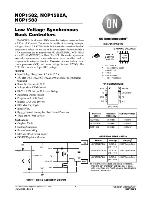
NCP1582, NCP1582A,NCP1583Low Voltage Synchronous Buck ControllersThe NCP158x is a low cost PWM controller designed to operate from a 5 V or 12 V supply. This device is capable of producing an output voltage as low as 0.8 V. This 8−pin device provides an optimal level of integration to reduce size and cost of the power supply. Features include a0.7 A gate driver and an internally set 350 kHz (NCP1582, NCP1582A) and a 300 kHz (NCP1583) oscillator. The NCP158x also incorporates an externally compensated transconductance error amplifier and a programmable soft−start function. Protection features include short circuit protection (SCP) and under voltage lockout (UVLO). The NCP158x comes in an 8−pin SOIC package.Features•Input V oltage Range from 4.5 V to 13.2 V•350 kHz (NCP1582, NCP1582A), 300 kHz (NCP1583) Internal Oscillator•Boost Pin Operates to 30 V•V oltage Mode PWM Control•0.8 V $1.5% Internal Reference V oltage•Adjustable Output V oltage•Programmable Soft−Start•Internal 0.7 A Gate Drivers•80% Max Duty Cycle•Input UVLO•R DS(on) Current Sensing for Short Circuit Protection •These are Pb−Free DevicesApplications•Graphics Cards•Desktop Computers•Servers/Networking•DSP and FPGA Power Supply•DC−DC Regulator ModulesFigure 1. Typical Application DiagramSOIC−8D SUFFIXCASE 7511MARKING DIAGRAMPIN CONNECTIONSx= 2, 2A or 3A= Assembly LocationL= Wafer LotY= YearW= Work WeekG= Pb−Free DeviceBST PHASETGGNDBGCOMP/DISFBV CC(Top View)Device Package Shipping†ORDERING INFORMATIONNCP1582DR2G SOIC−8(Pb−Free)2500/Tape & Reel†For information on tape and reel specifications, including part orientation and tape sizes, please refer to our T ape and Reel Packaging Specifications Brochure, BRD8011/D.NCP1582ADR2G SOIC−8(Pb−Free)2500/Tape & ReelNCP1583DR2G SOIC−8(Pb−Free)2500/Tape & Reel NCP158xSeriesOscillatorFrequencySCP Trip Voltage NCP1582350 kHz−350 mV NCP1582A350 kHz−450 mV NCP1583300 kHz−350 mVFigure 2. Typical VGA Card Application DiagramFigure 3. Detailed Block DiagramV CCTG BST PHASEBG GNDPIN FUNCTION DESCRIPTIONPin No.Symbol Description1BST Supply rail for the floating top gate driver. To form a boost circuit, use an external diode to bring thedesired input voltage to this pin (cathode connected to BST pin). Connect a capacitor (C BST) between this pinand the PHASE pin. Typical values for C BST range from 0.1 m F to 1 m F. Ensure that C BST is placed near the IC.2TG Top gate MOSFET driver pin. Connect this pin to the gate of the top N−Channel MOSFET.3GND IC ground reference. All control circuits are referenced to this pin.4BG Bottom gate MOSFET driver pin. Connect this pin to the gate of the bottom N−Channel MOSFET.5V CC Supply rail for the internal circuitry. Operating supply range is 4.5 V to 15 V. Decouple with a 1 m Fcapacitor to GND. Ensure that this decoupling capacitor is placed near the IC.6FB This pin is the inverting input to the error amplifier. Use this pin in conjunction with the COMP pin tocompensate the voltage−control feedback loop. Connect this pin to the output resistor divider (if used) ordirectly to Vout.7COMP/DIS Compensation Pin. This is the output of the error amplifier (EA) and the non−inverting input of the PWM comparator. Use this pin in conjunction with the FB pin to compensate the voltage−control feedback loop. Thecompensation capacitor also acts as a soft−start capacitor. Pull this pin low with an open drain transistor fordisable.8PHASE Switch node pin. This is the reference for the floating top gate driver. Connect this pin to the source of the top MOSFET.ABSOLUTE MAXIMUM RATINGSPin Name Symbol V MAX V MINMain Supply Voltage Input V CC15 V−0.3 VBootstrap Supply Voltage Input BST30 V wrt/GND15 V wrt/PHASE−0.3 VSwitching Node (Bootstrap Supply Return)PHASE24 V−0.7 V−5 V for < 50 nsHigh−Side Driver Output (Top Gate)TG30 V wrt/GND15 V wrt/PHASE−0.3 V wrt/PHASELow−Side Driver Output (Bottom Gate)BG15 V−0.3 V−2 V for < 200 ns Feedback FB 5.5 V−0.3 V COMP/DISABLE COMP/DIS 5.5 V−0.3 VMAXIMUM RATINGSRating Symbol Value Unit Thermal Resistance, Junction−to−Ambient R q JA165°C/W Thermal Resistance, Junction−to−Case R q JC45°C/W Operating Junction Temperature Range T J−40 to 150°C Operating Ambient Temperature Range T A−40 to 85°C Storage Temperature Range T stg−55 to +150°CLead Temperature Soldering (10 sec): Reflow (SMD styles only) Pb−Free(Note 1)260 peak°C Moisture Sensitivity Level MSL1−Stresses exceeding Maximum Ratings may damage the device. Maximum Ratings are stress ratings only. Functional operation above the Recommended Operating Conditions is not implied. Extended exposure to stresses above the Recommended Operating Conditions may affect device reliability.1.60−180 seconds minimum above 237°C.ELECTRICAL CHARACTERISTICS (0_C < T A < 70_C, −40_C < T J < 125_C (Note 2), 4.5 V < V CC < 13.2 V, 4.5 V < BST < 26.5 V, C TG= C BG= 1.0 nF(REF:NTD30N02), for min/max values unless otherwise noted.)Characteristic Conditions Min Typ Max Unit Input Voltage Range⎯ 4.513.2V Boost Voltage Range⎯ 4.526.5V Supply CurrentQuiescent Supply Current V FB = 1.0 V, No SwitchingV CC= 13.2 V− 1.0 1.75mA Boost Quiescent Current V FB = 1.0 V, No Switching−140−m A Under Voltage LockoutUVLO Threshold V CC Rising Edge 3.85 4.2V UVLO Hysteresis⎯−0.5V Switching RegulatorVFB Feedback Voltage, Control Loop in Regulation T A = 0 to 70°C−40 to 125°C0.7880.80.80.812VOscillator Frequency (NCP1582, NCP1582A)T A = 0 to 70°C−40 to 125°C300350350400kHzOscillator Frequency (NCP1583)T A = 0 to 70°C−40 to 125°C 275300300325kHzRamp−Amplitude Voltage− 1.1−V Minimum Duty Cycle−0−% Maximum Duty Cycle707580% Minimum Pulse Width Static Operating100150ns Blanking Time50ns BG Minimum On Time~500ns Error Amplifier (GM)Transconductance 5.0mmho Open Loop DC Gain5570−DBOutput Source Current Output Sink Current V FB = 0.8 VV FB > 0.8 V8080120120m Am AInput Offset Voltage−2.00 2.0mV Input Bias Current0.1 1.0m A Unity Gain Bandwidth 4.0Mhz Soft−StartSS Source Current V FB < 0.8 V 5.01015m A Switch Over Threshold100% of Vref Current LimitTrip Voltage (NCP1582, NCP1583)Vphase to ground−350mV Trip Voltage (NCP1582A)Vphase to ground−450mV Gate DriversUpper Gate Source Vgs = 6.0 V−0.7A Upper Gate Sink Vugate wrt Phase = 1.0 V 2.4W Lower Gate Source Vgs = 6.0 V−0.7A Lower Gate Sink Vlgate wrt GND = 1.0 V 2.2W PHASE Falling to BG Rising Delay V CC = 12 V, PHASE < 2.0 V, BG > 2.0 V−3090ns BG Falling to TG Rising Delay V CC = 12 V, BG < 2.0 V, TG > 2.0 V−3060ns Enable Threshold0.4V 2.Specifications to −40°C are guaranteed via correlation using standard quality control (SQC), not tested in production.TYPICAL OPERATING CHARACTERISTICSF S W , F R E Q U E N C Y (k H z )V r e f , R E F E R E N C E V O L T A G E (m V )−50−250255075100125T J , JUNCTION TEMPERATURE (°C)S O F T S T A R T S O U R C I N G C U R R E N T (m A )Figure 8. Soft Start Sourcing Current vs.TemperatureFigure 9. I−Limit vs. TemperatureT J , JUNCTION TEMPERATURE (°C)−50−250255075100125DETAILED OPERATING DESCRIPTION GeneralThe NCP158x is an 8−pin PWM controller intended forDC−DC conversion from 5.0 V & 12 V buses. The NCP158xhas a 0.7 A internal gate driver circuit designed to driveN−channel MOSFETs in a synchronous−rectifier bucktopology. The output voltage of the converter can beprecisely regulated down to 800 mV 1.5% when the V FB pinis tied to V OUT. The switching frequency is internally set. Ahigh gain operational transconductance error amplifier(OTA) is used.Duty Cycle and Maximum Pulse Width LimitsIn steady state DC operation, the duty cycle will stabilizeat an operating point defined by the ratio of the input to theoutput voltage. The NCP158x can achieve an 80% dutycycle. There is a built in off−time which ensures that thebootstrap supply is charged every cycle. The NCP158x,which is capable of a 100 nsec pulse width (min.), can allow a 12 V to 0.8 V conversion at 350 kHz.Input Voltage Range (V CC and BST)The input voltage range for both V CC and BST is 4.5 V to 13.2 V with respect to GND and PHASE, respectively. Although BST is rated at 13.2 V with respect to PHASE, it can also tolerate 26.5 V with respect to GND.External Enable/DisableWhen the Comp pin voltage falls or is pulled externally below the 400 mv threshold, it disables the PWM Logic and the gate drive outputs. In this disabled mode, the operational transconductance error amplifier’s (EOTA) output source current is reduced and limited to the Soft Start current of 10m A. Normal Shutdown BehaviorNormal shutdown occurs when the IC stops switching because the input supply reaches UVLO threshold. In this case, switching stops, the internal SS is discharged, and all GATE pins go low. The switch node enters a high impedance state and the output capacitors discharge through the load with no ringing on the output voltage.External Soft StartThe NCP158x features an external soft start function, which reduces inrush current and overshoot of the output voltage. Soft start is achieved by using the internal current source of 10 m A. (typ), which charges the external integrator capacitor of the transconductance amplifier. Figure 10 is a typical soft start sequence. This sequence begins once V CC surpasses its UVLO threshold. During Soft Start, as the Comp Pin rises through 400 mV, the PWM Logic and gate drives are enabled. When the feedback voltage crosses 800mV, the EOTA will be given control to switch to its higher regulation mode output current of 120m A. In the event of an overcurrent during soft start, the overcurrent logic will override the soft start sequence and will shut down the PWM logic and both the high side and low side gates.Figure 10. Soft Start ImplementationVEnableVIsource/SinkTiming Diagram NCP1582: Enable SequenceUVLOUnder V oltage Lockout (UVLO) is provided to ensure that unexpected behavior does not occur when V CC is too low to support the internal rails and power the converter. For the NCP158x, the UVLO is set to ensure that the IC will start up when V CC reaches 4.2 V and shutdown when V CC drops below 3.7 V. This permits operation when converting from a 5.0 input voltage.Current Limit ProtectionIn case of a short circuit or overload, the low−side (LS) FET will conduct large currents. The controller will shut down the regulator in this situation for protection against overcurrent. The low−side R DSon sense is implemented by comparing the voltage at the Phase node when BG starts going low to an internally generated fixed voltage. If the phase voltage is lower than SCP trip voltage, an overcurrent condition occurs and a counter is initiated. When the counter completes, the PWM logic and both HS−FET and LS−FET are turned off. The controller will retry to see if the short circuit or overload condition is removed through the soft start cycle. The minimum turn−on time of the LS−FET is set to be 500 ns. The trip thresholds have a −95 mV, +45 mV process and temperature variation.DriversThe NCP158x includes 0.7 A gate drivers to switch external N−channel MOSFETs. This allows the NCP158x to address high−power as well as low−power conversion requirements. The gate drivers also include adaptive non−overlap circuitry. The non−overlap circuitry increase efficiency, which minimizes power dissipation, by minimizing the body diode conduction time.A detailed block diagram of the non−overlap and gate drive circuitry used in the chip is shown in Figure 11.Figure 11. Block Diagram of Gate Driverand Non−Overlap CircuitryPHASETG BSTV CC BGGNDCareful selection and layout of external components is required, to realize the full benefit of the onboard drivers.The capacitors between V CC and GND and between BST and SWN must be placed as close as possible to the IC. The current paths for the TG and BG connections must be optimized. A ground plane should be placed on the closest layer for return currents to GND in order to reduce loop area and inductance in the gate drive circuit.APPLICATION SECTIONInput Capacitor SelectionThe input capacitor has to sustain the ripple current produced during the on time of the upper MOSFET, so it must have a low ESR to minimize the losses. The RMS value of this ripple is:Iin RMS +I OUT D (1*D)Ǹ,where D is the duty cycle, Iin RMS is the input RMS current,& I OUT is the load current. The equation reaches its maximum value with D = 0.5. Losses in the input capacitors can be calculated with the following equation:P CIN +ESR CIN Iin RMS 2,where P CIN is the power loose in the input capacitors &ESR CIN is the effective series resistance of the input capacitance. Due to large d I /d t through the input capacitors,electrolytic or ceramics should be used. If a tantalum must be used, it must be surge protected. Otherwise, capacitor failure could occur.Calculating Input Start−up CurrentTo calculate the input start up current, the following equation can be used.I inrush +C OUT V OUTt SS,where I inrush is the input current during start−up, C OUT is the total output capacitance, V OUT is the desired output voltage,and t SS is the soft start interval.If the inrush current is higher than the steady state input current during max load, then the input fuse should be rated accordingly, if one is used.Calculating Soft Start TimeTo calculate the soft start time, the following equation can be used.t SS +(C P )C C)*D VI SSWhere C C is the compensation as well as the soft start capacitor,C P is the additional capacitor that forms the second pole.I SS is the soft start currentD V is the comp voltage from zero to until it reachesregulation.V compV outThe above calculation includes the delay from comp rising to when output voltage becomes valid.To calculate the time of output voltage rising to when it reaches regulation; D V is the difference between the comp voltage reaching regulation and 1.1 V .Output Capacitor SelectionThe output capacitor is a basic component for the fast response of the power supply. In fact, during load transient,for the first few microseconds it supplies the current to the load. The controller immediately recognizes the load transient and sets the duty cycle to maximum, but the current slope is limited by the inductor value.During a load step transient the output voltage initial drops due to the current variation inside the capacitor and the ESR. (neglecting the effect of the effective series inductance (ESL)):D V OUT−ESR +D I OUT ESR COUT ,where V OUT−ESR is the voltage deviation of V OUT due to the effects of ESR and the ESR COUT is the total effective series resistance of the output capacitors.A minimum capacitor value is required to sustain the current during the load transient without discharging it. The voltage drop due to output capacitor discharge is given by the following equation:D V OUT−DISCHARGE +D I OUT 2 L OUT2 C OUT (V IN D *V OUT ),where V OUT−DISCHARGE is the voltage deviation of V OUT due to the effects of discharge, L OUT is the output inductor value & V IN is the input voltage.It should be noted that ΔV OUT−DISCHARGE and V OUT−ESR are out of phase with each other, and the larger of these two voltages will determine the maximum deviation of the output voltage (neglecting the effect of the ESL).Inductor SelectionBoth mechanical and electrical considerations influence the selection of an output inductor. From a mechanical perspective, smaller inductor values generally correspond to smaller physical size. Since the inductor is often one of the largest components in the regulation system, a minimum inductor value is particularly important in space−constrained applications. From an electrical perspective, the maximum current slew rate through the output inductor for a buck regulator is given by:SlewRate LOUT +V IN *VOUT L OUT.This equation implies that larger inductor values limit the regulator’s ability to slew current through the output inductor in response to output load transients. Consequently,output capacitors must supply the load current until the inductor current reaches the output load current level. Thisresults in larger values of output capacitance to maintain tight output voltage regulation. In contrast, smaller values of inductance increase the regulator’s maximum achievable slew rate and decrease the necessary capacitance, at the expense of higher ripple current. The peak−to−peak ripple current is given by the following equation:Ipk *pk LOUT +V OUT (1*D)L OUT 350kHz,where Ipk−pk LOUT is the peak to peak current of the output.From this equation it is clear that the ripple current increases as L OUT decreases, emphasizing the trade−off between dynamic response and ripple current.Feedback and CompensationThe NCP158x allows the output of the DC−DC converter to be adjusted from 0.8 V to 5.0 V via an external resistor divider network. The controller will try to maintain 0.8 V at the feedback pin. Thus, if a resistor divider circuit was placed across the feedback pin to V OUT , the controller will regulate the output voltage proportional to the resistordivider network in order to maintain 0.8 V at the FB pin.FBThe relationship between the resistor divider network above and the output voltage is shown in the following equation:R 2+R 1 ǒV REFV OUT *V REFǓ.Resistor R1 is selected based on a design tradeoff between efficiency and output voltage accuracy. For high values of R1 there is less current consumption in the feedback network, However the trade off is output voltage accuracy due to the bias current in the error amplifier. The output voltage error of this bias current can be estimated using the following equation (neglecting resistor tolerance):Error%+0.1m A R 1V REF100%.Once R1 has been determined, R2 can be calculated.Figure 12. Type II Transconductance ErrorAmplifierR C Figure 12 shows a typical Type II transconductance error amplifier (EOTA). The compensation network consists of the internal error amplifier and the impedance networks ZIN (R 1, R 2) and external Z FB (R c , C c and C p ). The compensation network has to provide a closed loop transfer function with the highest 0 dB crossing frequency to have fast response (but always lower than F SW /8) and the highest gain in DC conditions to minimize the load regulation. A stable control loop has a gain crossing with −20dB/decade slope and a phase margin greater than 45°. Include worst−case component variations when determining phase margin. Loop stability is defined by the compensation network around the EOTA, the output capacitor, output inductor and the output divider. Figure 13. shows the open loop and closed loop gain plots.Compensation Network Frequency:The inductor and capacitor form a double pole at the frequencyF LC +12p @L O @C OǸThe ESR of the output capacitor creates a “zero” at the frequency,F ESR +12p @ESR @C O The zero of the compensation network is formed as,F Z +12p @R C C CThe pole of the compensation network is calculated as,F P +12p @R C @C PFigure 13. Gain Plot of the Error AmplifierG A I N (d B )FREQUENCY (Hz)100100010 k100 k1000 kThermal ConsiderationsThe power dissipation of the NCP158x varies with the MOSFETs used, V CC , and the boost voltage (V BST ). The average MOSFET gate current typically dominates the control IC power dissipation. The IC power dissipation is determined by the formula:P IC +(I CC @V CC ))P TG )P BG .Where:P IC = control IC power dissipation,I CC = IC measured supply current,V CC = IC supply voltage,P TG = top gate driver losses,P BG = bottom gate driver losses.The upper (switching) MOSFET gate driver losses are:P TG +Q TG @f SW @V BST .Where:Q TG = total upper MOSFET gate charge at V BST ,f SW = the switching frequency,V BST = the BST pin voltage.The lower (synchronous) MOSFET gate driver losses are:P BG.Where:Q BG = total lower MOSFET gate charge at V CC .The junction temperature of the control IC can then be calculated as:T J +T A )P IC @q JA .Where:T J = the junction temperature of the IC,T A = the ambient temperature,θJA = the junction−to−ambient thermal resistance of the IC package.The package thermal resistance can be obtained from the specifications section of this data sheet and a calculation can be made to determine the IC junction temperature. However,it should be noted that the physical layout of the board, the proximity of other heat sources such as MOSFETs and inductors, and the amount of metal connected to the IC,impact the temperature of the device. Use these calculations as a guide, but measurements should be taken in the actual application.Layout ConsiderationsAs in any high frequency switching converter, layout is very important. Switching current from one power device to another can generate voltage transients across the impedances of the interconnecting bond wires and circuit traces. These interconnecting impedances should be minimized by using wide, short printed circuit traces. The critical components should be located as close together as possible using ground plane construction or single point grounding. The figure below shows the critical power components of the converter. To minimize the voltage overshoot the interconnecting wires indicated by heavy lines should be part of ground or power plane in a printed circuit board. The components shown in the figure below should be located as close together as possible. Please note that the capacitors C IN and C OUT each represent numerous physical capacitors. It is desirable to locate the NCP158x within 1inch of the MOSFETs, Q1 and Q2. The circuit traces for the MOSFETs’ gate and source connections from the NCP158x must be sized to handle up to 2 A peak current.Figure 14. Components to be Considered forLayout SpecificationsRETURNNCP1582, NCP1582A, NCP1583 Design ExampleSwitching Frequency F SW = 350 KHZOutput Capacitance C ESR = 45 m W/EachOutput Capacitance C out = 6630 m FOutput Inductance L out = 0.75 m HInput V oltage V in = 12 VOutput V oltage V out = 3.3 VChoose the loop gain crossover frequency;F CO+110*F SW+35kHzThe corner frequency of the output filter is calculatedbelow;F LC+12*p*0.75m H*6630m FǸ+2.3kHzLet R C = 1500Check that the ESR zero frequency is not too high;F ESR+12*p@CESR@C O t F SW5This condition is mandatory for loop stability.Zero of the compensation network is calculated as follows;F Z+F LCC C+1Z C+12*p*2.3kHz*1500+46nFThe compensation capacitor also acts as the soft start capacitor. By adjusting the value of this compensation capacitor, the soft start time can be adjusted.Pole of the compensation network is calculated as follows;F P+5*F CO+175kHzC P+12*p*F P*R C+12*p*175kHz*1500+700pFThe recommended compensation values are;R C = 1500, C C = 46 nF, C P = 700 pFThe NCP158x bode plot as measured from the network analyzer is shown below.Figure 15. Typical Bode plot of the Open−loop Frequency Response of the NCP158x Top plot: Phase−Frequency (Phase Margin = 62.519°) Bottom plot: Gain−Frequency (UGBW= 5 MHz)NCP1582, NCP1582A, NCP1583 Demo Board PCB LayoutBill of MaterialsItem Number Part Reference Value Quantity MFG 1C1 C2 C3 C41500 m F4PANASONIC 2C5 C6 C722 m F3TDK3C8 1.0 m F1TAIYO YUDEN 4C9100 pF1AVX5C100.022 m F1KEMET6C110.1 m F1AVX7C12 C13 C14 C151800 m F4PANASONIC 8C16 C17 C18 C1910 m F4KEMET9C20OPEN1−10C21OPEN1−11CR1BAS116LT11ON SEMICONDUCTOR 12L10.75 m H1TOKO13Q1 Q240N032ON SEMICONDUCTOR 14R14021DALE15R2OPEN1−16R3 1.02 K1DALE17R4OPEN1−18R6 R702DALE19R8OPEN1−20U1NCP158x1ON SEMICONDUCTORTYPICAL PERFORMANCE CHARACTERISTICSFigure 16. Start UpFigure 17. Gate Waveforms15 A Load SustainingFigure 18. Transient Response (0−10 A Step Load)8083868992123456789101112131415LOAD CURRENT (A)E F F I C I E N C Y (%)Figure 19. Transient ResponseFigure 20. Over Current Protection (22 A DC Trip)Figure 21. Efficiency vs. Load CurrentPACKAGE DIMENSIONSSOIC−8D SUFFIXCASE 751−07ISSUE AHNOTES:1.DIMENSIONING AND TOLERANCING PERANSI Y14.5M, 1982.2.CONTROLLING DIMENSION: MILLIMETER.3.DIMENSION A AND B DO NOT INCLUDEMOLD PROTRUSION.4.MAXIMUM MOLD PROTRUSION 0.15 (0.006)PER SIDE.5.DIMENSION D DOES NOT INCLUDE DAMBARPROTRUSION. ALLOWABLE DAMBARPROTRUSION SHALL BE 0.127 (0.005) TOTALIN EXCESS OF THE D DIMENSION ATMAXIMUM MATERIAL CONDITION.6.751−01 THRU 751−06 ARE OBSOLETE. NEWSTANDARD IS 751−07.DIMAMIN MAX MIN MAXINCHES4.805.000.1890.197MILLIMETERSB 3.80 4.000.1500.157C 1.35 1.750.0530.069D0.330.510.0130.020G 1.27 BSC0.050 BSCH0.100.250.0040.010J0.190.250.0070.010K0.40 1.270.0160.050M0 8 0 8N0.250.500.0100.020S 5.80 6.200.2280.244 YM0.25 (0.010)Z S X S____ǒmminchesǓSCALE 6:1*For additional information on our Pb−Free strategy and solderingdetails, please download the ON Semiconductor Soldering andMounting Techniques Reference Manual, SOLDERRM/D.SOLDERING FOOTPRINT*ON Semiconductor and are registered trademarks of Semiconductor Components Industries, LLC (SCILLC). SCILLC reserves the right to make changes without further notice to any products herein. SCILLC makes no warranty, representation or guarantee regarding the suitability of its products for any particular purpose, nor does SCILLC assume any liability arising out of the application or use of any product or circuit, and specifically disclaims any and all liability, including without limitation special, consequential or incidental damages.“Typical” parameters which may be provided in SCILLC data sheets and/or specifications can and do vary in different applications and actual performance may vary over time. All operating parameters, including “Typicals” must be validated for each customer application by customer’s technical experts. SCILLC does not convey any license under its patent rights nor the rights of others. SCILLC products are not designed, intended, or authorized for use as components in systems intended for surgical implant into the body, or other applications intended to support or sustain life, or for any other application in which the failure of the SCILLC product could create a situation where personal injury or death may occur. Should Buyer purchase or use SCILLC products for any such unintended or unauthorized application, Buyer shall indemnify and hold SCILLC and its officers, employees, subsidiaries, affiliates, and distributors harmless against all claims, costs, damages, and expenses, and reasonable attorney fees arising out of, directly or indirectly, any claim of personal injury or death associated with such unintended or unauthorized use, even if such claim alleges that SCILLC was negligent regarding the design or manufacture of the part. SCILLC is an Equal Opportunity/Affirmative Action Employer. This literature is subject to all applicable copyright laws and is not for resale in any manner.PUBLICATION ORDERING INFORMATION。
- 1、下载文档前请自行甄别文档内容的完整性,平台不提供额外的编辑、内容补充、找答案等附加服务。
- 2、"仅部分预览"的文档,不可在线预览部分如存在完整性等问题,可反馈申请退款(可完整预览的文档不适用该条件!)。
- 3、如文档侵犯您的权益,请联系客服反馈,我们会尽快为您处理(人工客服工作时间:9:00-18:30)。
Low Leakage
Pico Amp Diodes
JPAD5 / JPAD10 / JPAD20 / JPAD50 / JPAD100 / JPAD200
SSTPAD5 / SSTPAD10 / SSTPAD20 / SSTPAD50 / SSTPAD100 / SSTPAD200
FEATURES
•
Low Leakage. . . . . . . . . . . . . . . . . . . . . . . . 5 pA (JPAD5)
•
High Breakdown Voltage. . . . . . . . . . . . . . . -60 V typical•Low Capacitance. . . . . . . . . . . . . . . . . . . . . . . . . . . . 1.5 pfAPPLICATIONS•High Impedance Diode Switching•High Dynamic Range Log Amps•High Isolation Protection CircuitsDESCRIPTIONThe JPAD series is a low leakage, high speed diode used forinput protection circuitry and fast switching. These devices
are housed in a plastic TO-92 package for automated high
speed assembly. The design and processing of this series
results in very low leakage and low capacitance making it an
excellennt choice vs conventional diodes.
ORDERING INFORMATION
PartPackageTemperature Range
JPAD5-200Plastic TO-92-55
oC to +135o
C
SSTPAD5-200Plastic SOT-23-55
oC to +135o
C
XPAD5-200Sorted Chips in Carriers-55
oC to +135o
C
CORPORATION
PIN CONFIGURATION
SCHEMATIC DIAGRAM
A
C
TO-92
(MODIFIED)
PLASTIC
BOTTOM VIEW
A
C
A
C
PRODUCT MARKING (SOT-23)
SSTPAD5T05
SSTPAD10T10
SSTPAD20T20
SSTPAD50T50
SSTPAD100T11
SSTPAD200T21
SOT-23
A
C
5007, 5010
Note: Use only cathode "C" pin.
元器件交易网www.cecb2b.com
JPAD5 / JPAD10 / JPAD20 / JPAD50 / JPAD100 / JPAD200
SSTPAD5 / SSTPAD10 / SSTPAD20 / SSTPAD50 / SSTPAD100 / SSTPAD200
CORPORATION
ABSOLUTE MAXIMUM RATINGS (25oC)
Forward Current. . . . . . . . . . . . . . . . . . . . . . . . . . . . . . . . . . . . . . . . . . . . . . . . . . . . . . . . . . . . . . . . . . . . . . . . . . . . . . . . . . . . . . 10 mA
Total Device Dissipation . . . . . . . . . . . . . . . . . . . . . . . . . . . . . . . . . . . . . . . . . . . . . . . . . . . . . . . . . . . . . . . . . . . . . . . . . . . . . 360 mW
Storage Temperature Range. . . . . . . . . . . . . . . . . . . . . . . . . . . . . . . . . . . . . . . . . . . . . . . . . . . . . . . . . . . . . . . . . . . . . -55
oC to 125o
C
Lead Temperature (1/16" from case for 10 seconds). . . . . . . . . . . . . . . . . . . . . . . . . . . . . . . . . . . . . . . . . . . . . . . . . . . . . . . . . 300
o
C
ELECTRICAL CHARACTERISTICS (25
o
C Unless otherwise noted)
SYMBOLCHARACTERISTICSMINTYPMAXUNITTEST CONDITIONS
STATIC
I
RReverse Current PAD5-5pAVR
= -20 V
PAD10-10
PAD20-20
PAD50-50
PAD100-100
PAD200-200
B
VRBreakdown Voltage (Reverse)-35-60VIR
= -1mA
V
F
Forward Voltage Drop0.81.5VIF = 5 mA
DYNAMIC
C
RCapacitance1.52.0pFVR
= -5 V, f = 1 MHz
NOTE: Product available in surface mount SOT-23 upon request. Contact factory for further information.
元器件交易网www.cecb2b.com