UTCM3368中文资料
UTCMC3361BP中文资料
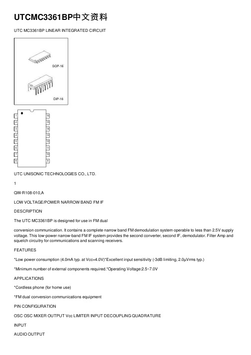
UTCMC3361BP中⽂资料UTC MC3361BP LINEAR INTEGRATED CIRCUITUTC UNISONIC TECHNOLOGIES CO., LTD.1QW-R108-010,ALOW VOLTAGE/POWER NARROW BAND FM IFDESCRIPTIONThe UTC MC3361BP is designed for use in FM dualconversion communication. It contains a complete narrow band FM demodulation system operable to less than 2.5V supply voltage. This low-power narrow-band FM IF system provides the second converter, second IF, demodulator. Filter Amp and squelch circuitry for communications and scanning receivers.FEATURES*Low power consumption (4.0mA typ. at Vcc=4.0V)*Excellent input sensitivity (-3dB limiting, 2.0µVrms typ.)*Minimum number of external components required.*Operating Voltage:2.5~7.0VAPPLICATIONS*Cordless phone (for home use)*FM dual conversion communications equipmentPIN CONFIGURATIONOSC OSC MIXER OUTPUT Vcc LIMITER INPUT DECOUPLING QUADRATUREINPUTAUDIO OUTPUTFILTER INPUT FILTER OUTPUT SCAN CONTROLSQUELCH INPUTMUTEGNDRF INPUT DECOUPLINGUTC MC3361BP LINEAR INTEGRATED CIRCUITUTC UNISONIC TECHNOLOGIES CO., LTD.2QW-R108-010,AABSOLUTE MAXIMUM RATINGS (TA=25°C)PARAMETERSYMBOLVALUEUNITMax. Supply Voltage Vcc(max)10V Supply Voltage Range Vcc 2.5 to 7.0V Detector Input voltage V I(DET) 1.0Vp-p RF Input Voltage (Vcc>=4.0V)V I(RF) 1.0Vrms Mute Function V MUTE -0.5 ~ + 5.0Vpeak Operating Temperature T OPR -20 to +70°C Storage Temperature T STG -65 to +150°CNote: Absolute maximum ratings are those values beyond which permanent damage to the device may occur. These are stress ratings only and functional operation of the device at or beyond them is not implied. Long exposure to these conditions may affect device reliability.ELECTRICAL CHARACTERISTICS(Vcc=4.0V, fo=10.7MHz,?f=+-3KHz,Ta=25°C, unless otherwise specified)PARAMETER SYMBOL TEST CONDITIONS MIN TYP MAX UNIT Operating CurrentIcc Squelch off (V12=2V)Squelch on (V12=GND)4.06.0mA Input Limiting voltageV I(LIM)-3.0dB limiting2.0µV Detector Output voltage V O(DET) 2.0Vdc Detector Output Impedance Z O(DET)400?Audio Output Voltage V OVin=10mV 100160mVrms Filter GainG V f=10KHz,Vin=5mV 4048dB Filter Output DC Voltage V O(DC) 1.5Vdc Trigger Hysteresis of filter V TH 50mV Mute Switch-on Resistance RON(MUTE)Mute “Low”10?Mute Switch-off Resistance R OFF(MUTE)Mute “High”10M ?Scan Control “Low” Output V L(SCAN)Mute off (V12=2V)0.5Vdc Scan Control “High” Output V H(SCAN)Mute on (V12=GND)3.0Vdc Mixer Conversion GainG V(MIXER)24dB Mixer Input Resistance R I(MIXER) 3.3K ?Mixer Input CapacitanceC I(MIXER)2.2pFUTC MC3361BP LINEAR INTEGRATED CIRCUITUTC UNISONIC TECHNOLOGIES CO., LTD.3QW-R108-010,AAPPLICATION CIRCUITIn the above typical application, the audio signal is recovered using a conventional quadrature FM detector. Theabsence of an input signal is indicated by the presence of noise above the desired audio frequencies. This “noise band: is monitored by an active filter and a detector. A squelch trigger circuit indicates the presence of noise (or a tone) by an output which can be used to control scanning. At the same time, an internal switch is operated which can be used to mute the audio.TOKO TYPE RMC-2A6597HM0.1µOUT M U R A T A。
美国蒙那多Monarch ACT-3X 中文说明书

ACT-3X转速计/累加器/速率表用户手册1.0版,021110版合测实业保障措施和注意事项1.请仔细阅读并遵守本手册中的所有说明,并保留此手册供将来参考。
2.请勿以与本使用说明书不符的任何方式使用本仪器,也不得以超出上述环境规格的任何条件使用本仪器。
3.确保提供给本仪器的电源符合后面板上的规定。
4.在连接本仪器或从本仪器取下任何连接之前,请确保所有的交流电源都已拆除。
5.该仪器不是用户可维修的。
如需技术支持,请直接联系您购买产品的销售机构或MonarchInstrument。
为了遵守关于报废电子电气设备(WEEE)的欧盟指令2002/96 / EC:本产品可能含有可能危害人体健康和环境的物质。
请勿将本产品作为未分类的城市垃圾进行处理。
该产品需要根据当地法规进行回收,请联系当地有关部门以获取更多信息。
目录1.0总体概述 .....................................................................................................1 2.0 安装 (1)2.1嘈杂的环境 .................................................................................................................... 1 2.2调整 ............................................................................................................................... 2 2.3 连接 . (2)2.3.1 电源连接 (2)2.3.2 传感器连接 (2)2.3.3 模拟输出 (3)2.3.4 辅助输入(AUX-通道2) (3)2.3.5 脉冲输出 (3)2.3.6 报警继电器输出 (3)2.3.7 串行通信 (4)3.0 前面板 .........................................................................................................4 3.1 状态指示灯 .. (4)3.1.1 LIM 1和LIM 2(报警)LED (4)3.1.2 GATE LED (4)3.1.3 MAX和MIN LED (4)3.1.4 RPM LED (4)3.2 按按钮 (4)3.2.1 设置按钮 (4)3.2.2 复位按钮 (4)3.2.3 向上( )和向下( )按钮 (5)3.2.4 回拨按钮 (5)4.0 操作 ............................................................................................................5 4.1 操作模式 - 频道1 (5)4.1.1 RPM模式 (5)4.1.2 频率模式 (5)4.1.3 比例模式(比率计) (5)4.1.4 单事件捕获(SECAP)模式 (5)4.1.5 变化率(ROC)模式 (5)4.1.6 累计模式 (6)4.2操作模式 - 频道2 (6)4.2.1 离 . (6)合测实业4.2.2 抑制 (6)4.2.3 单事件捕获 (6)4.2.4 外部复位 - 输入累加器 (6)4.2.5 外部复位 - 报警 (6)4.3 小数点 (6)4.4 警报限制 (6)4.4.1 锁定与非锁定限制 (6)4.4.2 死区(滞后) (7)4.4.3 低限锁定 (7)4.4.4 失败安全 (7)4.5 模拟(AO)和电流(IO)输出 (7)4.6 最大值和最小值 (7)4.7 吞吐量 (7)4.7.1 显示更新率 (8)4.7.2 内部更新率 - GATE (8)4.7.3 低端 (8)4.8 脉冲输出 (8)5.0 使用菜单 (8)5.1 (9)5.1.1 (9)5.1.2 (9)5.1.3 (9)5.1.4 . (9)5.2 (9)5.2.1 . (9)5.2.2 (10)5.3 (10)5.4 (10)5.4.1 (10)5.4.2 . (10)5.4.3 (10)5.4.4 (10)5.4.5 (10)5.4.6 (10)5.5 (10)5.6 (10)5.6.1 (11)5.6.2 (11)5.6.3 (11)5.7 (11)5.8 (11)5.9 (11) (11)5.10 ...........................................................5.11 ................................... (11) (11)5.12 .......6.0 SERIAL OUTPUT (11)6.1 来自串行接口的数据 (11)6.2 串行命令 (12)6.2.1 运行模式命令 (12)6.2.2 控制命令 (12)7.0 规格 (14)8.0 选件和附件/传感器 (15)附录A - 缩放工程显示的行为 (16)附录B - 有用的转换 (17)附录C - 使用单事件捕获模式 (18)附录D - 菜单概览 (19)1.0 总体概述ACT-3X数字表是一种非常通用的仪器。
UTCLMV358中文资料

UTC LMV358LINEAR INTEGRATED CIRCUITUTC UNISONIC TECHNOLOGIES CO.,LTD.1QW-R105-010,AGENERAL PURPOSE, LOWVOLTAGE, RAIL-TO-RAIL OUTPUTOPERATIONAL AMPLIFIERSDESCRIPTIONThe UTC LMV358 are low voltage (2.7-5.5V) versions of the dual and quad commodity op amps, LM358, which currently operate at 5-30V. The LMV358 are the most cost effective solutions for the applications where low voltage operation,space saving and low price are needed. They offer specifications that meet or exceed the familiar LM358. The LMV358 have rail-to-rail output swing capability and the input common-mode voltage range includes ground. They alll exhibit excellent speed-power ratio, achieving 1 MHz of bandwidth and 1 V/µs of slew rate with low supply current. The chips are built with National’s advanced submicron silicon-gate BiCMOS process. The LMV358 have bipolar input and output stages for improved noise performance and higher output current drive.FEATURES(For V 1 =5V and V=0V. Typical Unless Otherwise Noted)*Guaranteed 2.7V and 5V Performance *No Crossover Distortion *Space Saving Package *Industrial Temp. Range *Gain-Bandwidth Product *Low Supply Current: 210µA *Rail-to-Rail Output Swing @10k Ω Load V 1-10mV V +65mV *V CM -0.2V to V 1 –0.8VAPPLICATIONS*Active Filters*General Purpose Low Voltage Applications *General Purpose Portable DevicesPIN CONFIGURATIONS12348765OUT BIN B-IN A+V-V+OUT A IN A-IN B+ABUTC LMV358LINEAR INTEGRATED CIRCUITUTC UNISONIC TECHNOLOGIES CO.,LTD.2QW-R105-010,AABSOLUTE MAXIMUM RATINGSPARAMETERVALUE UNIT ESD Tolerance(Note 2) Machine Model 100V Human Body Model 2000VDifferential Input Voltage +-Supply VoltageSupply Voltage (V 1-V) 5.5VOutput Short Circuit to V 1(Note 3)Output Short Circuit to V (Note 4)Mounting Temp.Lead Temp. (Soldering 10 sec)260°C Infrared (15 sec)215°C Storage Temp. Range-65 to 150°C Junction Temp. (Tj, max) (Note 5)150°COPERATING RATINGS (NOTE 1)PARAMETERVALUE UNIT Supply Voltage 2.7 to 5.5V Temperature Range-40<=Tj<=85°C Thermal Resistance (θJA ) (Note 10)235°C/W2.7V DC ELECTRICAL CHARACTERISTICSUnless otherwise specified, all limits guaranteed for Tj=25°C, V 1=2.7V, V=0V, V CM =1.0V, Vo=V 1/2 and RL=1M ΩPARAMETERSYMBOL CONDITIONSTYP (note6)LIMIT (note7)UNIT Input Offset VoltageVos 1.77mV max Input Offset Voltage Average Drift TCVos 5µV/°C Input Bias Current Is 11250nA max Input Offset CurrentIos 550nA max Common Mode Rejection Ratio CMRR 0V<=V CM <=1.7V 6350dB min Power Supply Rejection Ratio PSRR 2.7V<=V 1 <=5VVo=1V 6050dB min Input Common-Mode Voltage RangeV CMFor CMRR>=50dB-0.20V min 1.91.7V max Output Swing Vo RL=10k Ω to 1.35V V 1-10V 1-100mV min 60180mV max Supply Current Is Both amplifiers 140340µAUTC LMV358LINEAR INTEGRATED CIRCUITUTC UNISONIC TECHNOLOGIES CO.,LTD.3QW-R105-010,APARAMETERSYMBOLCONDITIONSTYP (note6)LIMIT (note7)UNIT max2.7V AC ELECTRICAL CHARACTERISTICSUnless otherwise specified, all limits guaranteed for Tj=25°C, V 1=2.7V, V=0V, V CM =1.0V, Vo=V 1/2 and RL>1M ΩPARAMETERSYMBOL CONDITIONS TYP (note6)LIMIT (note7)UNIT Gain-Bandwidth Product GBWP CL=200pF1MHz Phase Margin Φ(T)60Deg Gain MarginG(r)10dB Input-Referred Voltage Noise θr1F=1kHz 46nV √ Hz Input-referred Current NoiseIr1F=1kHz0.17pA √ Hz5V DC ELECTRICAL CHARACTERISTICSUnless otherwise specified, all limits guaranteed for Tj=25°C, V 1=5V, V=0V, V CM =2.0V, Vo=V 1/2 and RL>1M Ω.Boldface limits apply at the temperature extremes.PARAMETERSYMBOL CONDITIONS TYP LIMIT UNIT Input Offset VoltageVos 1.779mV max Input Offset Voltage Average Drift TCVos 5µV/°C Input Bias Current IB 15250500nA max Input Offset CurrentIos 550150nA max Common Mode Rejection Ratio CMRR 0V<=V CM <=4V 6550dB min Power Supply Rejection Ratio PSRR 2.7V<=V 1<=5V Vo=1V V CM =1V 6050dB min Input Common-Mode Voltage RangeV CMFor CMRR>=50dB-0.20V min 4.24V max Large Signal Voltage Gain(Note 8)Av RL=2k Ω1001510V/mV min Output SwingVoRL=2k Ω to 2.5VV 1-40V 1-300V +-400mV min 120300400mV max Vo RL=10k Ω to 2.5V V 1-10V 1-100V +-200mV min 65180280mV max Output Short Circuit Current Io Sourcing,Vo=0V 605mA minUTC LMV358LINEAR INTEGRATED CIRCUITUTC UNISONIC TECHNOLOGIES CO.,LTD.4QW-R105-010,APARAMETERSYMBOLCONDITIONS TYP LIMIT UNIT Sinking,Vo=5V16010mA min Supply CurrentIsBoth amplifiers210440615µA max2.5V AC ELECTRICAL CHARACTERISTICSUnless otherwise specified, all limits guaranteed for Tj=25°C, V 1=2.7V, V=0V, V CM =2.0V, Vo=V 1/2 and RL>1M ΩPARAMETERSYMBOL CONDITIONS TYP LIMIT UNIT Slew RateSR (Note 9)1V/µs Gain-Bandwidth Product GBWP CL=200pF1MHz Phase Margin Φ(T)60Deg Gain MarginG(r)10dB Input-Referred Voltage Noise θr1f=1kHz 39nV √ Hz Input-referred Current NoiseIr1f=1kHz0.21pA √ HzNote1:Absolute Maximum Ratings indicate limits beyond which damage to the device may occur. Operating Ratings indicate conditions for which the device is intended to be functional, but specific performances is not guaranteed. For guaranteed specifications and the test conditions, see the Electrical Characteristics.Note2:Human body model 1.5k Ω in series with 100pF. Machine model, 0Ω in series with 200pF.Note3:Shorting output to V 1 will adversely after reliability.Note4:Shorting output to V + will adversely affect reliability.Note5:The maximum power dissipation is a function of Tj(max) θJA and TA. The maximum allowable powerdissipation at any ambient temperature is PD=(Tj(max)-TA)/θJA. All numbers apply for packages soldered directly into a PC board.Note6:Typical values represent the most likely parametric norm.Note7:All limits are guaranteed by testing or statistical analysis.Note8:RL is connected to V. The output voltages is 0.5V<=Vo<=4.5V.Note9:Connected as voltage follower with 3V step input. Number specified is thes lower of the positive andnegative slew rates.Note10:all numbers are typical, and apply for packages soldered directly note a PC board is still air.UTC LMV358LINEAR INTEGRATED CIRCUITUTC UNISONIC TECHNOLOGIES CO.,LTD.5QW-R105-010,ATYPICAL PERFORMANCE CHARACTERISTICS(Unless otherwise specified,V E =+5V,single supply. TA=25°C)UTC LMV358LINEAR INTEGRATED CIRCUITUTC UNISONIC TECHNOLOGIES CO.,LTD.6QW-R105-010,AUTC LMV358LINEAR INTEGRATED CIRCUITUTC UNISONIC TECHNOLOGIES CO.,LTD.7QW-R105-010,AUTC LMV358LINEAR INTEGRATED CIRCUITUTC UNISONIC TECHNOLOGIES CO.,LTD.8QW-R105-010,AUTC LMV358LINEAR INTEGRATED CIRCUITUTC UNISONIC TECHNOLOGIES CO.,LTD.9QW-R105-010,A。
UTCTA7738P中文资料

UTC TA7738P LINEAR INTEGRATED CIRCUITUTC UNISONIC TECHNOLOGIES CO., LTD.1QW-R110-009,AAMPLIFIER SYSTEM FORCASSETTE TAPE RECORDERDESCRIPTIONThe UTC TA7738P is an amplifier system, designed for a stereo set and a radio cassette tape recorder.FEATURES*Recorder play balk for pre-amplifier *Buffer amplifier( recorder amplifier)*Power amplifier*Wide operating voltage range( 3.5V to 9V)BLOCK DIAGRAMBufferOutput Buffer NFGNDPower Input Power NFPowerGNDPower OutputPre OutputPre NFPre InputPre GNDFilter 2Filter 1VccBoot StrapALC InputABSOLUTE MAXIMUN RATING (Ta=25°C)PARAMETER SYMBOLVALUEUNITSupply Voltage VCC 14V Output Current I O(peak) 1.5A Power Dissipation*PD 1200mW Operating TemperatureTOPR-25~75°C Storage Temperature TSTG-55~150°C*Note: De-rated above Ta=25°C in proportion of 9.6mW/°CUTC TA7738P LINEAR INTEGRATED CIRCUITUTC UNISONIC TECHNOLOGIES CO., LTD.2QW-R110-009,AELECTRONIC CHARACTERISTICS (Ta=25°C, V CC =6V, f=1kHZ, unless otherwise specified)PARAMETER SYMBOL TEST CONDITIONS MIN TYP MAXUNITTotalQuiescent Current I CCQ1VCC=3.5V 7.5mAI CCQ2VCC=6V1135Pre-amplifierOpen Loop Voltage Gain G VO15570dB Closed Loop Voltage Gain G V140dB Maximum Output Voltage V OUT1THD<1%0.7Vrms Input Impedance R IN1VOUT=0.5Vrms30k ΩEquivalent Input Noise VoltageV NIRg=01.42.5µΩVrmsPre-amplifier + Buffer amplifier Closed Loop Voltage Gain G V2Pre-AMP GV=40dB Buff-AMP GV=20dB60dBMaximum Output Voltage V OUT2THD=3% 1.51.7Vrms Equivalent Input Noise Voltage V NO2Rg=0, GV2=60dB1.22.5mVrmsALC Effect A LC1VIN= -60dBm~ -20dBm2dB ALC Range A LC2THD<1%60dBPower amplifierOpen Loop Voltage Gain G VO16070dB Closed Loop Voltage Gain G V140dB Maximum Output Power P OM RL=4Ω,THD=10%0.80.96WVCC=9V,RL Ω,THD=10%2Output Noise VoltageV NO3Rg=0, GV=40dB0.31mVrmsUTC TA7738P LINEAR INTEGRATED CIRCUIT TEST CIRCUITSWITCH MODETEST ITEM SW1SW2SW3SW4SW5SW6 GVO111ON OFF OFF OFFGV111OFF OFF OFF OFFVOUT111OFF OFF OFF OFFGV213OFF OFF OFF OFFVOUT213OFF OFF OFF OFFVNO213OFF OFF ON OFFALC12OFF OFF OFF OFFGVO321OFF ON OFF OFFGV321OFF OFF OFF OFFPO21OFF OFF OFF OFFVNO321OFF OFF OFF ON UTC UNISONIC TECHNOLOGIES CO., LTD.3QW-R110-009,AUTC TA7738P LINEAR INTEGRATED CIRCUITUTC UNISONIC TECHNOLOGIES CO., LTD.4QW-R110-009,ATYPICAL PERFORMANCE CHARACTERISTICS1THD vs Output Power 11P0(W)THD vs Output Power 2110f(Hz)Po(W)Vcc(V)Double Channel Mode Output Powervs Supply VoltageTHD vs Output FrequencyPO(W)。
UC3838 友顺UTC 电子元器件芯片

UNISONIC TECHNOLOGIES CO., LTDUC3838Preliminary CMOS IC LOW COST POWER-SAVINGMODE PWM CONTROLLERFOR FLYBACK CONVERTERSDESCRIPTIONThe UTC UC3838provides a CCM switching mixed modeoperation for better efficiency performance. The operation modestays at CCM at heavy load, and switch to power-saving mode atlight load.The UTC UC3838is a high performance current mode PWMcontroller ideally suited for low standby power. Low V CC startupcurrent make the power reliable on startup design and a largevalue resistor could be used in the startup circuit to minimize thestandby power. At no load condition, the IC operates inpower-saving mode for lower standby power, decreasing frequencyfor Higher conversion efficiency at light load condition.The UTC UC3838contains protection with automatic recoveryincluding OLP (over load protection), OCP (cycle-by-cycle currentlimiting), and UVLO (V CC over voltage clamp and under voltagelockout). It also provides the protections including OTP (overtemperature protection), OVP (V CC or DC output over voltageprotection) with automatic recovery. To protect the powerMOSFET, Gate-drive output is fixed up to 17V max.The internal slope compensation improves system stability athigh PWM duty cycle output. Leading-edge blanking on currentsense input removes the signal glitch, which offering minimaexternal component count in the design. Excellent EMIperformance is achieved with UTC propriet ary frequency hoppingtechnique together with soft driver control. Audio noise iseliminated due to switch frequency more than 20kHz duringoperation.UTC UC3838 is packaged by using tiny SOT-26 package. It hassuch applications as: battery charger, power adaptor, set-top boxpower supplies, ink jet printers, open-frame SMPS.FEATURES*Proprietary frequency hopping for Improved EMI performance*Cycle-by-cycle current limiting*CCM Power-saving mode Switching Operation*Fixed switch frequency 65kHz TYP.*Dynamic peak current limiting for constant output power*Built-in synchronized slope compensation*Gate output voltage clamped at 17V*Adjustable DC output OVP/OTP*OLP/V CC OVP/Internal OTP (automatic recovery)*Internal Soft Start*OTP through a NTC (latch mode)ORDERING INFORMATIONMARKINGPIN CONFIGURATIONPIN DESCRIPTIONBLOCK DIAGRAMABSOLUTE MAXIMUM RATINGAbsolute maximum ratings are stress ratings only and functional device operation is not implied. RECOMMENDED OPERATING CONDITIONSTHERMAL DATAELECTRICAL CHARACTERISTICS (V CC=15V, T A=25°C, unless otherwise specified)ELECTRICAL CHARACTERISTICS (Cont.)APPLICATION NOTEThe UTC UC3838 devices integrate many useful designs into one controller for low-power switch-mode power supplies. The following descriptions highlight some of the features of the UTC UC3838 series. Start-up CurrentThe start-up current is only 1μA. Low start-up current allows a start-up resistor with a high resistance and a low-wattage to supply the start-up power for the controller. For AC/DC adaptor with universal input range design, a 2.5~3MΩ, startup resistor could be used together with a V CC capacitor to provide a fast startup and low powerdissipation solution. The D1 IN4148 can improve surge capability to 6.6KV.Fig. 1 Startup CircuitOperation ModeThe UTC UC3838 provides a CCM switching mixed mode operation for better efficiency performance. The operation mode stays at CCM at heavy load, once if the converter enters into DCM, the UTC UC3838automaticallyfinds the local minimum VDSpoint and switching at this local.Normally, the conduction loss is dominated at heavy load condition, and the switching loss turns to be larger than conduction loss in light load, especially at 1/4 ~ 1/2 of full load. By this kind of mixed mode operation to have CCM inheavy load and switching in light load can optimize the overall average efficiency during the entire operation range.APPLICATION NOTE (Cont.)As shown in Fig. 3, at deep light-load or no-load condition, the switching loss is the dominant factor. To improve the light-load efficiency, burst mode operation will stop the switching cycle of the OUT pin when FB pin voltage is below “V FB_IN” Level and restart the switching cycle of the OUT pin when FB pin voltage is above “V FB_OUT”.Over Voltage Protection on V CC Pin ( V CC OVP )The V CC OVP will shut down the switching of the power MOSFET whenever V CC>V OVP. The OVP event as followed Fig.4.Fig.4 OVP case Fig.5 OLP caseOver Load &Open Loop & Output Short Protection ( OLP or OSP )OLP or OSP will shut down driver when V FB> V OLP for continual a blanking time. The OLP or OSP event as followed Fig.5.Over Temperature Protection ( OTP )OTP will shut down driver when the NTC resistor temperature T J>T (THR).Pull this pin below 0.95V to shutdown the controller into latch mode until AC power-on againAPPLICATION NOTE (Cont.)Adjustable OTP & OVP Protection on OTP PINThe OTP circuit is implemented to sense whether there is any hot-spot of power circuit like power MOSFET or output rectifier. Once an over-temperature condition is detected, the OTP is enabled to shut down the controller to protect the controller. Typically, a NTC is recommended to connect with OTP pin. The NTC resistance will decrease as the device or ambient in high temperature. The relationship is as below.NTCOTP R ×A μ100=V When the V OTP is below the defined voltage threshold (typ. 0.95V), UTC UC3838 will shutdown the gate output and latch off the power supply. There are 2 conditions required to restart it successfully. First, cool down the circuit so that NTC resistance will increase and raise V OTP up above 1.05V. Then, VCC recovery, until AC power-on again An over voltage protection for OTP pin is fulfilled by monitoring the voltage V CC1 after the zener connected in series to the VCC. When V CC1 exceeds V OTP_OVP (typ. 4.28V), output will shutdown until AC power-on again.Z+OVP _OTP )OVP (CC V V =VFig. 6 OTP-Pin ProtectionAPPLICATION NOTE (Cont.)Cycle by Cycle Over-Current Protection (OCP)In a Flyback topology converter, the main MOSFET switch of the Flyback converter turns on and off rapidly. The energy is stored in the inductor when the MOSFET turns on. The inductor current flowing through the sensing resistor (R CS ) is shown in Fig.7. The current limit is determined by the equation below:CSCS MAX _PEAK R V =I In order to prevent the CS pin from false triggering, an internal leading edge blanking time (350nS Typ.) is added and an external low pass RC filter is also recommended to filter the turn-on spike of CS node.In general, the power converter can deliver more current at high input voltage than at low input voltage. To compensate this, an offset voltage is added to the CS signal by an internal current source (I OCP ) and an external resistor (R OCP ) in series between the sense resistor (Rcs) and the CS pin, as shown in Fig.8. By selecting a proper value of the resistor in series with the CS pin, the amount of compensation can be adjusted. The value of I OCP depends on the duty cycle of OUT pin. The relation curve between I OCP and duty is shown in Figure 7.Fig. 7 Current SensingFig. 8 AC input Compensation ON CS-PINAPPLICATION NOTE (Cont.)In light load conditions, the offset should be removed since it is in same order of magnitude as the current sense signal. Therefore the compensation current is only fully added when the FB voltage is higher than 2.27V. R OCP: 470~1.2k, C OCP: 47pF~390pF.An output overvoltage protection is implemented in the UTC UC3838, as shown in Fig. 9. It senses the auxiliary voltage via the divided resistors. The auxiliary winding voltage is reflected from secondary winding and therefore the flat voltage on the CS pin is proportional to the output voltage. UTC UC3838 can sample this flat voltage level after a delay time to perform output over voltage protection. This delay time is used to ignore the voltage ringing from leakage inductance of PWM transformer. The sampling voltage level is compared with internal threshold voltage 0.2V. If the sampling voltage exceeds the OVP trip level, an internal counter starts counting subsequent OVP events. The counter has been added to prevent incorrect OVP detection which might occur during ESD or lightning events. However, when typically 7 cycles of subsequent OVP events are detected, the OVP circuit switches the power MOSFET off. As the protection is occur, the converter only restarts after VCC auto-recovery.(a)Out(b)Fig. 9 DCOVP ON CS-PINAPPLICATION NOTE (Cont.)MOSFET CharacteristicThe MOSFET is divided into three operation regions, ohmic region, saturation region, and the cut-off region, shown as Fig. 10(a). For switching power supply applications, it shall operate in ohmic and cut-off region. Never reach the region of saturation; it would cause damage for acting beyond the maximum safety operating area. It’s necessary to check the characteristic of MOSFET. Fig.10(c) shows a totem pole architecture for the circuit of OUT. The output high level of OUT is at around V CC-1.5V. Refer to on-region characteristics of the MOSFET, check the saturation current of V GS H(MIN) to make sure the saturation current is high enough to activate MOSFET to operate in ohmic region. In order not to decrease the voltage across V G, it’s recommended not to connect a forward diode between the gate of the MOSFET and OUT pin, for example like Fig.10(d) . In addition, pulling V CC level high can keep V GSH in high level, for example:(1). Increase NX value to pull V CC level high. (2). Increase V CC capacitance to improve V CC’s performance to drop at startup transient, shown as Fig.10(b) .(a)(b)RS(c) (d)Fig.10 MOSFET CharacteristicTYPICAL APPLICATION CIRCUIT。
UTCLM7809中文资料

UTC LM78XXLINEAR INTEGRATED CIRCUITUTC UNISONIC TECHNOLOGIES CO., LTD.1QW-R101-006,C3-TERMINAL 1A POSITIVE VOLTAGE REGULATORDESCRIPTIONThe UTC 78XX family is monolithic fixed voltageregulator integrated circuit. They are suitable for applications that required supply current up to 1 A.FEATURES*Output current up to 1.5 A*Fixed output voltage of 5V, 6V, 8V, 9V, 10V, 12V, 15V ,18V and 24V available*Thermal overload shutdown protection *Short circuit current limiting*Output transistor SOA protection1: Input 2: GND 3: OutputTEST CIRCUITINPUTZ1UTC LM78XXLINEAR INTEGRATED CIRCUITUTC UNISONIC TECHNOLOGIES CO., LTD.2QW-R101-006,CABSOLUTE MAXIMUM RATINGS( Operating temperature range applies unless otherwise specified )PARAMETER SYMBOL RATING UNITInput voltage(for Vo=5~18V)(for Vo=24V) V I 35 40V V Output CurrentI o 1 A Power DissipationPD Internally Limited W Operating Junction Temperature RangeT OPR-20+150°CStorage Temperature Range T STG -55+150 °C UTC LM7805 ELECTRICAL CHARACTERISTICS( VI=10V, Io=0.5A, Tj= 0°C - 125°C, C1=0.33uF, Co=0.1uF, unless otherwise specified )(Note 1)PARAMETERSYMBOLTEST CONDITIONSMINTYP MAX UNITTj=25°C, I O =5mA - 1.0A4.805.0 5.20 VOutput Voltage VoV I =7.5V to 20V, I O =5mA - 1.0A,PD<15W4.755.25 V Load Regulation∆Vo Tj =25°C,I O =5mA - 1.5A 50 mVTj=25°C,I O =0.25A - 0.75A 25 mVLine regulation ∆Vo V I =7V to 25V,Tj=25°C 50 mVV I =7.5V to 20V,Tj=25°C,Io=1A 50 mV Quiescent Current Iq Tj=25°C, I O =<1A 8.0 mAQuiescent Current Change ∆Iq V I =7.5V to 20V 1.0 mA∆Iq I O =5mA - 1.0A 0.5 mA Output Noise Voltage V N 10Hz<=f<=100kHz 40 µV Temperature coefficient of Vo ∆Vo/∆T Io =5mA -0.6mV/°C Ripple Rejection RR V I =8V - 18V,f=120Hz,Tj=25°C 6280 dB Peak Output Current I PK Tj=25°C 1.8 A Short-Circuit Current I SC VI=35V, Tj=25°C 250 mA Dropout Voltage Vd Tj=25°C 2.0 VUTC LM7806 ELECTRICAL CHARACTERISTICS( VI=11V, Io=0.5A, Tj= 0°C - 125°C, C1=0.33uF, Co=0.1uF, unless otherwise specified )(Note 1)PARAMETERSYMBOLTEST CONDITIONSMINTYP MAX UNITTj=25°C, I O =5mA - 1.0A5.766.0 6.24 V Output VoltageVoV I =8.5V to 21V,I O =5mA - 1.0A, PD<15W5.706.30 VLoad Regulation∆Vo Tj =25°C,I O =5mA - 1.5A 60 mVTj=25°C,I O =0.25A - 0.75A 30 mVLine regulation ∆Vo V I =8V to 25V,Tj=25°C 60 mVV I =8.5V to 21V,Tj=25°C,Io=1A 60 mV Quiescent Current Iq Tj=25°C, I O =<1A 8.0 mAQuiescent Current Change ∆Iq V I =8.5V to 21V 1.0 mA∆Iq I O =5mA - 1.0A 0.5 mA Output Noise Voltage V N 10Hz<=f<=100kHz 45 µV Temperature coefficient of Vo ∆Vo/∆T Io =5mA -0.7mV/°C Ripple RejectionRR V I =9V - 19V,f=120Hz,Tj=25°C 5975 dBUTC LM78XXLINEAR INTEGRATED CIRCUITUTC UNISONIC TECHNOLOGIES CO., LTD.3QW-R101-006,CPARAMETERSYMBOLTEST CONDITIONSMINTYP MAX UNITPeak Output Current I PK Tj=25°C 1.8 AShort-Circuit Current I SCVI=35V, Tj=25°C 250 mA Dropout Voltage VdTj=25°C 2.0 VUTC LM7808 ELECTRICAL CHARACTERISTICS( VI=14V, Io=0.5A, Tj= 0°C - 125°C, C1=0.33uF, Co=0.1uF, unless otherwise specified )(Note 1)PARAMETERSYMBOL TEST CONDITIONSMINTYP MAX UNITTj=25°C, I O =5mA - 1.0A 7.688.0 8.32 V Output VoltageVoV I =10.5V to 23V,I O =5mA - 1.0A, PD<15W7.608.40 VLoad Regulation ∆Vo Tj =25°C,I O =5mA - 1.5A 80 mVTj=25°C,I O =0.25A - 0.75A 40 mVLine regulation ∆Vo V I =10.5V to 25V,Tj=25°C 80 mVV I =10.5V to 23V,Tj=25°C,Io=1A 80 mV Quiescent Current Iq Tj=25°C, I O =<1A 8.0 mAQuiescent Current Change ∆Iq V I =10.5V to 23V 1.0 mA ∆Iq I O =5mA - 1.0A 0.5 mAOutput Noise Voltage V N 10Hz<=f<=100kHz 58 µVTemperature coefficient of Vo ∆Vo/∆T Io =5mA -0.9mV/°C Ripple Rejection RR V I =11.5V to 21.5V, f=120Hz,Tj=25°C 5672 dBPeak Output Current I PK Tj=25°C 1.8 A Short-Circuit Current I SC VI=35V, Tj=25°C 250 mA Dropout Voltage Vd Tj=25°C 2.0 VUTC LM7809 ELECTRICAL CHARACTERISTICS( VI=15V, Io=0.5A, Tj= 0°C - 125°C, C1=0.33uF, Co=0.1uF, unless otherwise specified )(Note 1)PARAMETERSYMBOLTEST CONDITIONSMINTYP MAX UNITTj=25°C, I O =5mA - 1.0A8.649.0 9.36 VOutput Voltage VoV I =11.5V to 24V, I O =5mA - 1.0A,PD<15W8.55 9.45 V Load Regulation ∆Vo Tj =25°C,I O =5mA - 1.5A 90 mVTj=25°C,I O =0.25A - 0.75A 45 mVLine regulation ∆Vo V I =11.5V to 25 V, Tj=25°C, PD<15W90 mVV I =11.5V to 24V,Tj=25°C, Io<=1A90 mV Quiescent Current Iq Tj=25°C, I O =<1A 8.0 mAQuiescent Current Change ∆Iq V I =11.5V to 24V 1.0 mA∆Iq I O =5mA – 1.0A 0.5 mA Output Noise Voltage V N 10Hz<=f<=100kHz 58 µV Temperature coefficient of Vo ∆Vo/∆T Io =5mA -1.1 mV/°C Ripple Rejection RR V I =12.5V to 22.5V, f=120Hz,Tj=25°C 5672 dBPeak Output Current I PK Tj=25°C 1.8 A Short-Circuit Current I SC VI=35V, Tj=25°C 250 mA Dropout Voltage Vd Tj=25°C 2.0 VUTC LM78XXLINEAR INTEGRATED CIRCUITUTC UNISONIC TECHNOLOGIES CO., LTD.4QW-R101-006,CUTC LM7810 ELECTRICAL CHARACTERISTICS( VI=16V, Io=0.5A, Tj= 0°C - 125°C, C1=0.33uF, Co=0.1uF, unless otherwise specified )(Note 1) PARAMETERSYMBOLTEST CONDITIONSMINTYP MAX UNITTj=25°C, I O =5mA - 1.0A9.6010.0 10.40 V Output Voltage Vo VI =12.5V to 25V,I O =5mA - 1.0A,PD<=15W9.5010.50 VLoad Regulation ∆Vo Tj =25°C,I O =5mA - 1.5A 100 mVTj=25°C,I O =0.25A - 0.75A 50 mVLine regulation ∆Vo VI =13V to 25V,Tj=25°C 100 mVVI =13V to 25V, Tj=25°C,Io<=1A 100 mVQuiescent Current Iq Tj=25°C, I O =<1A 8.0 mAQuiescent Current Change ∆Iq VI =12.6V to 25V 1.0 mA ∆Iq I O =5mA - 1.0A 0.5 mAOutput Noise Voltage V N 10Hz<=f<=100kHz 58 µVTemperature coefficient of Vo ∆Vo/∆T Io =5mA -1.1mV/°C Ripple Rejection RR VI =13V - 23V,f=120Hz,Tj=25°C 5672 dBPeak Output Current I PK Tj=25°C 1.8 A Short-Circuit Current I SC VI=35V, Tj=25°C 250 mA Dropout Voltage Vd Tj=25°C 2.0 VUTC LM7812 ELECTRICAL CHARACTERISTICS( VI=19V, Io=0.5A, Tj= 0°C - 125°C, C1=0.33uF, Co=0.1uF, unless otherwise specified )(Note 1)PARAMETER SYMBOLTEST CONDITIONS MIN TYP MAX UNITTj=25°C, I O =5mA - 1.0A 11.5212.0 12.48 VOutput Voltage VoV I =14.5V to 27V,I O =5mA - 1.0A,PD<15W11.40 12.60 V Load Regulation∆Vo Tj =25°C,I O =5mA - 1.5A 120 mVTj=25°C,I O =0.25A - 0.75A 60 mVLine regulation ∆Vo V I =14.5V to 30V,Tj=25°C 120 mVV I =14.6V to 27V,Tj=25°C, Io=1A120 mV Quiescent Current Iq Tj=25°C, I O =<1A 8.0 mAQuiescent Current Change ∆Iq V I =14.5V to 30V 1.0 mA∆Iq I O =5mA - 1.0A 0.5 mA Output Noise Voltage V N 10Hz<=f<=100kHz 75 µV Temperature coefficient of Vo ∆Vo/∆T Io =5mA -1.5mV/°C Ripple Rejection RR V I =15V - 25V,f=120Hz,Tj=25°C 5572 dB Peak Output Current I PK Tj=25°C 1.8 A Short-Circuit Current I SC VI=35V, Tj=25°C 250 mA Dropout Voltage Vd Tj=25°C 2.0 VUTC LM78XXLINEAR INTEGRATED CIRCUITUTC UNISONIC TECHNOLOGIES CO., LTD.5QW-R101-006,CUTC LM7815 ELECTRICAL CHARACTERISTICS( VI=23V, Io=0.5A, Tj= 0°C - 125°C, C1=0.33uF, Co=0.1uF, unless otherwise specified )(Note 1)PARAMETERSYMBOLTEST CONDITIONSMINTYP MAX UNITTj=25°C, I O =5mA - 1.0A14.4015.0 15.60 V Output VoltageVoV I =17.5V to 30V,I O =5mA - 1.0A,PD<15W 14.2515.75 VLoad Regulation ∆Vo Tj =25°C,I O =5mA - 1.5A 150 mVTj=25°C,I O =0.25A - 0.75A 75 mVLine regulation ∆Vo V I =18.5V to 30V,Tj=25°C 150 mVV I =17.7V to 30V, Tj=25°C, I O =1A 150 mV Quiescent Current Iq Tj=25°C, I O =<1A 8.0 mAQuiescent Current Change ∆Iq V I =17.5V to 30V 1.0 mA ∆Iq I O =5mA - 1.0A 0.5 mAOutput Noise Voltage V N 10Hz<=f<=100kHz 90 µVTemperature coefficient of Vo ∆Vo/∆T Io =5mA -1.8mV/°C Ripple Rejection RR V I =18.5V to 28.5V f=120Hz,Tj=25°C5470 dBPeak Output Current I PK Tj=25°C 1.8 A Short-Circuit Current I SC VI=35V, Tj=25°C 250 mA Dropout Voltage Vd Tj=25°C 2.0 VUTC LM7818 ELECTRICAL CHARACTERISTICS( VI=27V, Io=0.5A, Tj= 0°C - 125°C, C1=0.33uF, Co=0.1uF, unless otherwise specified )(Note 1)PARAMETERSYMBOLTEST CONDITIONSMINTYP MAX UNITTj=25°C, I O =5mA - 1.0A17.2818.0 18.72 VOutput Voltage VoV I =21V to 33V,I O =5mA - 1.0A 17.1018.90 V Load Regulation∆Vo Tj =25°C,I O =5mA - 1.5A 180 mVTj=25°C,I O =0.25A - 0.75A 90 mVLine regulation ∆Vo V I =21V to 33V,Tj=25°C 180 mVV I =21V to 33V,Tj=25°C, I O =<1A,PD<15W 180 mV Quiescent Current Iq Tj=25°C, I O =<1A 8.0 mAQuiescent Current Change ∆Iq V I =21.5V to 33V 1.0 mA∆Iq I O =5mA - 1.0A 0.5 mA Output Noise Voltage V N 10Hz<=f<=100kHz 110 µV Temperature coefficient of Vo ∆Vo/∆T Io =5mA -2.2mV/°C Ripple Rejection RR V I =22V - 32V,f=120Hz,Tj=25°C 5369 dB Peak Output Current I PK Tj=25°C 1.8 A Short-Circuit Current I SC VI=35V, Tj=25°C 250 mA Dropout Voltage Vd Tj=25°C 2.0 VUTC LM78XXLINEAR INTEGRATED CIRCUITUTC UNISONIC TECHNOLOGIES CO., LTD.6QW-R101-006,CUTC LM7824 ELECTRICAL CHARACTERISTICS( VI=33V, Io=0.5A, Tj= 0°C - 12°C, C1=0.33uF, Co=0.1uF, unless otherwise specified )(Note 1)PARAMETERSYMBOLTEST CONDITIONSMINTYP MAX UNITTj=25°C, I O =5mA - 1.0A23.0424.0 24.96 VOutput VoltageVoV I =27V to 38V,I O =5mA - 1.0A 22.8025.20 V Load Regulation ∆Vo Tj =25°C,I O =5mA - 1.5A 240 mVTj=25°C,I O =0.25A - 0.75A 120 mVLine regulation ∆Vo V I =27V to 38V,Tj=25°C 240 mVV I =27V to 38V,Tj=25°C,Io=1A 240 mV Quiescent Current Iq Tj=25°C, I O =<1A 8.0 mAQuiescent Current Change ∆Iq V I =28V to 38V 1.0 mA ∆Iq I O =5mA - 1.0A 0.5 mAOutput Noise Voltage V N 10Hz<=f<=100kHz 170 µVTemperature coefficient of Vo ∆Vo/∆T Io =5mA -2.8mV/°C Ripple Rejection RR V I =28V - 38V,f=120Hz,Tj=25°C 5066 dB Peak Output Current I PK Tj=25°C 1.8 A Short-Circuit Current I SC VI=35V, Tj=25°C 250 mA Dropout Voltage Vd Tj=25°C 2.0 VNote 1: The Maximum steady state usable output current are dependent on input voltage, heat sinking, lead lengthof the package and copper pattern of PCB. The data above represents pulse test conditions with junction temperatures specified at the initiation of test.Note 2: Power dissipation<0.5WAPPLICATION CIRCUITNote 1: To specify an output voltage, substitute voltage value for "XX".Note 2: Bypass capacitors are recommended for optimum stability and transient response and should be located asclose as possible to the regulators.。
UTCNE556中文资料

UTC NE556LINEAR INTEGRATED CIRCUITUTC UNISONIC TECHNOLOGIES CO., LTD.1QW-R106-002,ADUAL TIMERDESCRIPTIONThe UTC NE556 dual monolithic circuit is a highlystable controller capable of producing accurate delays or oscillation. The UTC NE556 is the dual of UTC NE555; timing is provided an external resistor and capacitor for each function. The two timers operate independently of each other, sharing only Vcc and GND. The circuits may be triggered and reset on falling wave forms. The output structures may sink or source 200mA.FEATURES*High current driver capability(=200mA)*Adjustable duty cycle*Timing from µSec to Hours*Temperature stability of 0.005%/°C *TTL compatible*Operates in both Astable and Monostable modesAPPLICATIONS*Precision timing.*Pulse width modulation.*Pulse generator, shaping. *Traffic light control.*Time delay generator.*Touch tone encoder.*Sequential timing.*Tone burst generator.BLOCK DIAGRAMUTC NE556LINEAR INTEGRATED CIRCUITUTC UNISONIC TECHNOLOGIES CO., LTD.2QW-R106-002,AABSOLUTE MAXIMUM RATINGS (Ta=25°C )PARAMETERSYMBOL VALUE UNIT Supply Voltage Vcc 16V Power DissipationPd 600mW Lead Temperature(soldering 10sec.)Tlead 300°C Operating Temperature Topr -40~85°C Storage TemperatureTstg-65~150°CELECTRICAL CHARACTERISTICS( Ta=25°C ,Vcc=5 to 15V, unless otherwise specified )PARAMETER SYMBOL TEST CONDITIONS MIN TYP MAX UNIT Supply voltageVcc 4.516V Supply Current(two timers)IccVcc=5V,RL=∝512mA (low state), (Note 1)Vcc=15V,RL=∝1630mA Timing Error(monostable)Initial Accuracy(Note 2)A CCURR A =2K Ω to 100K ΩC=0.1µF T=1.1RC0.75%Drift with Temperature ∆t/∆T 50ppm/°C Drift with Supply Voltage ∆t/∆Vcc 0.1%/V Timing Error(astable)Initial Accuracy(Note 2)A CCURR A =1K Ω to 100K ΩC=0.1µF Vcc=15V2.25%Drift with Temperature ∆t/∆T 150ppm/°C Drift with Supply Voltage ∆t/∆Vcc 0.3%/V Control Voltage Vc Vcc=15V 9.010.011.0V Vcc=5V 2.6 3.33 4.0V Threshold Voltage V TH Vcc=15V 8.810.011.2V Vcc=5V 2.4 3.33 4.2V Threshold Current(Note 3)I TH 30250nA Trigger Voltage Vtr Vcc=5V 1.1 1.6 2.2V Vcc=15V 4.55 5.6V Trigger CurrentItr Vtr=00.01 2.0µA Reset Voltage(Note 4)Vrst 0.40.6 1.0V Reset CurrentIrst 0.030.6mA Low Output VoltageV OLVcc=15VIsink=10mA Isink=50mA Isink=100mA Isink=200mA0.10.25V0.40.75V 2 3.2V 2.5VVcc=5VIsink=5mA Isink=8mA0.150.25V 0.250.35VHigh Output VoltageV OHVcc=15VIsource=200mA Isource=100mAUTC NE556LINEAR INTEGRATED CIRCUITUTC UNISONIC TECHNOLOGIES CO., LTD.3QW-R106-002,APARAMETERSYMBOLTEST CONDITIONSMIN TYP MAX UNIT 12.5V 12.7513.3VVcc=5VIsource=100mA2.753.3V Rise Time of Output t R 100300nSec Fall Time of Outputt F 100300nSec Discharge Leakage Current I LKG 20100nA Matching Parameter Initial Accuracy(Note 5)A CCURR A, R B =1K Ω to 100K ΩC=0.1µF Vcc=15V12%Drift with Temperature ∆t/∆T 10ppm/°C Drift with Supply Voltage ∆t/∆Vcc 0.20.5%/VNote 1: Supply current when output is high is typically 1mA less at Vcc 5V.Note 2: Tested at Vcc=5V and Vcc=15V.Note 3: This will determine the maximum value of RA+RB for 15V operation, The maximum total is R=20M Ω, and for 5V operation the maximum total is R=6.6M Ω.Note 4: As reset voltage lower, timing is inhibited and then the output goes low.Note 5: Matching parameters refer to the difference between performance parameters of each timer section in the monostable mode.。
UTC34018中文资料

IV+ VCC VCCLN ROVCC VCCSAT VB ROVB
ç )
V+=11V,18 =0.7V V+=11V,18 =1.6V V+=7.5V 6.5V<V+<11V ICC=3.0mA V+=5.0V V+=7.5V IB=1.7mA 1.0KHZ 24 =VB,27 =250mVrms
DIP-28
౧$-
/ÅPͩ$ 28 ඥ (DIP) (0.6 &
˷.
)
--ሓ -) - ֧ ç -ᇗ
/ ç
ÅP
- ᇍ
9
9 ළ"
ɢ ܰ -ሓ ܰ ঠVcc )
ç
֧
ᇗˣ )ඥ
ऋᇗˣ
ˋƢᇗˣ /ÅP
c
Ѥ
1
c
Ѥ
ˤ
87&
˷.
-ᇗ
ඥ
ऋᇗˣ
+
0.068µF 100kΩ 4.7kΩ 47µF 4.7µF 47µF 200kΩ
0.01µF
0.01µF Vcc 4.7µF 0.068µF 3.3kΩ 0.068µF 47µF 100kΩ 0.068µF 1.0µF VB 3.3kΩ 0.1µF
VB 0.05µF
0.1µF S2
4.7kΩ
-)
3
TXI
10
MCO
13
XDI
4
TXO
5
TLI
11
CP1
25
ACF
17
AGC
470kΩ
Ρ
V V V V k k
ȉ
- 1、下载文档前请自行甄别文档内容的完整性,平台不提供额外的编辑、内容补充、找答案等附加服务。
- 2、"仅部分预览"的文档,不可在线预览部分如存在完整性等问题,可反馈申请退款(可完整预览的文档不适用该条件!)。
- 3、如文档侵犯您的权益,请联系客服反馈,我们会尽快为您处理(人工客服工作时间:9:00-18:30)。
UTC M3368
LINEAR INTEGRATED CIRCUIT
UTC UNISONIC TECHNOLOGIES CO., LTD.
1
QW-R124-003,A
3-INPUT VIDEO SWITCH WITH 6dB AMPLIFIER
DESCRIPTION
The UTC M3368 is three input integrated video switch witch selects one video or audio signal from three input signals.
It contains 6dB amplifier and its operating supply voltage range is 4.75 to 13V and bandwidth is 5MHz.Crosstalk is 65dB (at 4.43MHz)
FEATURES
*Operating Voltage: 4.75 to 13V *3 Input-1 Output
*Internal 6dB Amplifier *Muting Function available *Internal Clamp Function
*Cross-talk 65dB (at 4.43MHz)
*Wide Frequency Range 5MHz (1Vp-p Input)
APPLICATION
*VCR, AV -TV, Video Disc Player
*Pb-free plating product number: M3368L
PIN CONFIGURATION
V in 1SW1SW2
V +GND V in 2V in 3
Vout
UTC M3368
LINEAR INTEGRATED CIRCUIT
UTC UNISONIC TECHNOLOGIES CO., LTD.
2
QW-R124-003,A
BLOCK DIAGRAM
GND Vout V +Vin3(Mute)V in 1
SW1
V in 2
SW2
INPUT CONTROL SIGNAL-OUTPUT SIGNAL
SW1 SW2
OUTPUT SIGNAL
L L Vin1 H L Vin2 L/H
H
Vin3
Note: Input clamp voltage is about 2/5 of supply voltage
ABSOLUTE MAXIMUM RATINGS (Ta=25℃)
PARAMETER SYMBOL RATINGS
UNIT
Supply Voltage
V
+
15 V Power Dissipation
DIP-8 SOP-8 P D 500 300 mW Operating Temperature Range Topr -40 ~ +85 °C Storage Temperature Range
Tstg
-40 ~ +125 °C
UTC M3368
LINEAR INTEGRATED CIRCUIT
UTC UNISONIC TECHNOLOGIES CO., LTD.
3
QW-R124-003,A
ELECTRICAL CHARACTERISTICS (V +=5V,Ta=25℃)
PARAMETER SYMBOL
TEST CONDITION
MIN TYP MAX
UNIT Recommended Supply Voltage
V +
4.75
13.0 V
Operating Current Icc S1=S2=S3=S4=S5=2 9.514.0 21.0 mA
Voltage Gain
Gv Vin=1.0Vp-p, 1MHz, Vo/Vi, R L =1k Ω 5.5 6.0 6.5 dB Frequency Characteristic Gf Vin=1.0Vp-p, Vo(10MHz)/Vo(1MHz)R L =1k Ω -1.0 +1.0 dB Differential Gain DG Vin=1.0Vp-p, staircase, R L =1k Ω 0.3 % Differential Phase DP Vin=1.0Vp-p, staircase, R L =1k Ω 0.3 deg. Output Offset Voltage Voff S1=S2=S3=2, S5=1→2, Vo:voltage change ±60 mV Crosstalk
CT Vin=1Vp-p, 4.43MHz, Vo/Vi -65 dB V CH All inside SW: ON 2.4
Switch Change Voltage
V CL All inside SW: OFF 0.8
V
Note: Unless specified,tested with three mode below.
(a) S1=1, S2=S3=S4=S5=2 (b) S2=S4=1, S1=S3=S5=2 (c) S1=S2=2, S3=S5=1, S4=1 or 2
APPLICATION
Oscillation Prevention on light loading conditions Recommended under circuit.
This IC requires 1M Ω resistance between INPUT and GND pin for clamp type input since the minute current causes an unstable pin voltage.
LPF
V OUT 7
r 100 C 20pF
UTC M3368
LINEAR INTEGRATED CIRCUIT
UTC UNISONIC TECHNOLOGIES CO., LTD.
4
QW-R124-003,A
TEST CIRCUIT
V +GND
Vo
Vo
UTC M3368LINEAR INTEGRATED CIRCUIT
UTC UNISONIC TECHNOLOGIES CO., LTD. 5
QW-R124-003,A
UTC M3368
LINEAR INTEGRATED CIRCUIT
UTC UNISONIC TECHNOLOGIES CO., LTD.
6
QW-R124-003,A
APPLICATION
This IC requires 1M Ω resistance between INPUT and GND pin for clamp type input since the minute current causes an unstable pin voltage.
INPUT
F
This IC requires 0.1μF capacitor between INPUT and GND ,1M Ω resistance between INPUT and GND for clamp type input at mute mode.
INPUT
C 0.1 F r 1M。