A1852 Datasheet VER1.2
MBI1801 Datasheet VA.01- CN
*模拟时,PCB尺寸为76.2mm*114.3mm。请参考JEDEC JESD 51标准。 **越接近此最大范围值操作,IC的寿命越短、可靠度越低;超过此最大限定范围工作时,将会影响IC运作并造成毁损, 因此建议的IC工作时的接合点温度在125°C以内。 注:散热表现是与散热片面积、PCB层数与厚度相关。实测热阻值会与模拟值有所不同。使用者应根据所欲达到的散 热表现,选择合适的封装与PCB布局,以增加散热能力。
-8-
2012 年 9 月, VA.01
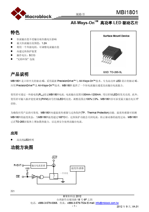
MBI1801
“Pb-Free & Green”封装之焊接制程*
All-Ways-OnTM 高功率 LED 驱动芯片
聚积科技所生产的“Pb-Free & Green"的半导体产品遵循欧洲 RoHS 标准,封装选用 100%之纯锡以兼容于目前锡铅 (SnPb)焊接制程,且支持需较高温之无铅制程。纯锡目前已被欧美及亚洲区的电子产品客户与供货商广泛采用,成为 取代含锡铅材料的最佳替代品。100%纯锡可生产于含锡铅(SnPb)锡炉制程,锡炉温度请参考 JEDEC J-STD-020C 标 准规定。 但若客户使用完全无铅锡膏和材料, 则锡炉温度须达 J-STD-020C 标准之 245°C 至 260°C (参阅下图)。 材料, 则锡炉温度须达 J-STD-020C 标准之 245°C 至 260°C (参阅下图)。
OE =高电位时耐受电压
输出端电流 输入端电压 输出端漏电流 输出电流1 电流偏差量 输出电流 2 电流偏差量 电流偏差量 vs. 输出电压 电流偏差量 vs. 电源电压 Pull-up电阻
=17V, OE =High
VDS= 0.6V IOUT= 488mA VDS= 0.6V VDS= 0.8V IOUT= 976mA VDS= 0.8V
OCP8155 datasheet

设计PCB时遵循以下几点: (1) VCC的旁路电容要紧靠芯片VCC引脚 (2) 电流采样电阻的功率地线尽可能短,和其它地线分头接到BULK电容的地端。 (3) 尽可能减小大电流环路的面积,以减小EMI辐射。 (4) FB脚的分压电阻要尽可能靠近FB脚。
Page 7 - 9
Ver 1.1 April. 01, 2013
3. 恒流设置
芯片通过将CS端的电压与内部1V阈值电压进行比较来设定变压器原边峰值电流Ipkp:
I pkp
=
1 RCS
LED输出电流IO根据如下公式计算:
Io
=
1* 6
np ns
* I pkp
其中Ipkp为原边峰值电流,np为变压器原边的匝数,ns为变压器副边的匝数。
(5) (6)
4. 元件参数设置
19
18.75
18.5
18.25
18
17.75
17.5 -40
-10
20
50
80
110
140
Temperature(℃)
过压保护电压对温度的变化
1.1
1.08
1.06
1.04
1.02
1
0.98
0.96
0.94
0.92
0.9 9
10
11
12
13
14
15
16
VCC(V)
CS 门限电压对 VCC 的变化
CH1:CS CH2:VBULK CH4:IOUT 系统上电各节点波形
通过上述两个方面的考虑,选择结果中较小的一个VOR值。
根据以下公式计算原边和副边匝比:
n p = VOR ns VO
EUM6861 Datasheet

18VDESCRIPTIONEUM6861/A/B is a fan motor driver for the single coil brushless DC motor. With its high efficient direct PWM control mode, EUM6861/A/B controls the speed of brushless DC motor with a built in HALL IC interface. EUM6861/A/B is suitable to drive variable speed motors for personal computer’s power supply radiation fans and CPU coolers.EUM6861/A/B integrates PWM fan speed control, minimum speed mode, soft start, fan tachometer, lock protection, auto restart and Hall Bias functions. PWM mode controls fan speed in low noise and low vibration ways by adjusting RCTL voltage. EUM6861/A/B can set minimum fan speed by presetting RMIN voltage. With soft start function, EUM6861/A/B can drive motor from slow speed to fast speed in a settable time by setting the external capacitor between SS and GND. If a fan motor is stalled by the external force or obstacles, overdrive current may incur coil overheat and burning. To prevent motor from overheating, the lock protection circuit shuts down the internal power devices for a few seconds after the motor lock is detected. Then the auto restart circuit resumes to power up the internal power devices. If the lock persists, EUM6861/A/B shuts off power devices for a few seconds. The lock protection delay time is externally programmable by a capacitor. EUM6861 has built in motor rotation speed feedback (FG) output, motor rotation detection (RD) output and Hall sensor bias output.Application Circuit z Built in 18V Full-wave Motor Driver for Fan Motorz Built in Input Surge Protection, No Zener Diode Needz External Programmable Soft Start and Soft Restart Functionz Wide Input Range 3V~18V z PWM Fan Speed Controlz Programmable Minimum Fan Speed z Built in Soft Switching Function z Built in Hall Biasz Lock Protection and Auto Restartz Fan Rotation Speed Feedback FG Output (EUM6861/B)z Fan Rotation Detection RD Output (EUM6861/A)z Thermal Shutdown Protectionz Available in TSSOP-16 and TDFN-14 Packages zRoHS Compliant and 100% Lead (Pb)-Free Halogen-FreeAPPLICATIONSz Personal Computer’s Power Supply Radiation Fans and CPU CoolersFigure 1. TSSOP -16 Typical Application CircuitApplication Circuit (continued)Figure 2. TDFN-14 Typical Application Circuit Functional Block DiagramFigure 3. Functional Block DiagramPin ConfigurationsPackage TypePin Configurations Package TypePin ConfigurationsEUM6861 TSSOP-16EUM6861A TDFN-14EUM6861B TDFN-14Pin DescriptionPIN EUM6861EUM6861AEUM6861BDESCRIPTIONPGND 1,16-- Power device groundOUT2 2 1 1Power device output terminal 2. Connect OUT2 to one side ofthe motor3 - - Power supply of internal control circuitry and power devicesVCC- 3 3 Power supply of internal control circuitryRMIN 4 4 4 Motor minimum rotation speed control RCTL 5 5 5 Motor rotation speed control CPWM 6 6 6 External capacitor connection input for PWM OSC FG 7 - 7 Rotation speed feedback output RD 8 7 - Rotation detection output IN+ 9 8 8 Hall sensor positive input HB 10 9 9 Hall sensor bias output IN- 11 10 10 Hall sensor negative input SS 12 11 11 Soft start time setting terminal CT 13 13 13 Lock protection time setup input14 - - Analog control circuit groundGND - Thermal Pad ThermalPadIC groundOUT1 15 14 14Power device output terminal 1. Connect OUT1 to the otherside of the motor.PVCC - 2 2 Power supply of power devices REG - 12 12 6V regulatorOrdering InformationOrder Number Package Type Marking Operating Temperature Range-30°C to +90°C EUM6861QIR1TSSOP-16 xxxxxEUM6861-30°C to +90°C EUM6861AJIR1TDFN-14xxxxxM6861-30°C to +90°C EUM6861BJIR1TDFN-14xxxxx6861BEUM6861/A/B □□□□Lead Free Code1: Lead Free, Halogen Free 0: LeadPackingR: Tape & ReelOperating temperature rangeI: Industry StandardPackage TypeQ: TSSOPJ: TDFNPower DissipationFigure 4. TSSOP-16 PackageFigure 5. TDFN-14 PackageAbsolute Maximum Ratings (1)VCC, RD, FG , OUT1, OUT2 to GND ------------------------------------------------- -0.3V to 30V RMIN, RCTL to GND --------------------------------------------------------------------- -0.3V to 7V CPWM, SS, CT, IN+, IN-, HB to GND ---------------------------------------------- -0.3V to 6V PGND to GND ------------------------------------------------------------------------- -0.3V to +0.3V IOUT1, IOUT2----------------------------------------------------------------------------------- 1.0A IHB, IFG , IRD ------------------------------------------------------------------------------------- 10mAMaximum Junction Temperature ------------------------------------------------------------ +150°CLead Temperature (Soldering, 10sec.) ------------------------------------------------------ +300°C Package Thermal Resistance θJA (TSSOP-16) --------------------------------------------- 157°C/W Package Thermal Resistance θJA (TDFN-14) ---------------------------------------------- 110°C/W Power Dissipation P D @ T A =+25°C (TSSOP-16) ------------------------------------------ 0. 8W Power Dissipation P D @ T A =+25°C (TDFN-14) ------------------------------------------- 1.14W Storage Temperature --------------------------------------------------------------- -55°C to +150°C ESD RatingsHuman Body Mode ------------------------------------------------------------------------------- 2kVThermal Shut Down----------------------------------------------------------------------------- 180°C Recommended Operating Conditions (2)Supply V oltage VCC --------------------------------------------------------------------- 3V to 16V Threshold Input V oltage RCTL, RMIN ------------------------------------------------ 0V to 6V Hall Input V oltage Range IN+, IN- ------------------------------------------------------ 0.2V to 3VOperating Temperature Range ------------------------------------------------------ -30°C to +90°CNote (1): Stress beyond those listed under “Absolute Maximum Ratings” may damage the device. Note (2): The device is not guaranteed to function outside the recommended operating conditions.Electrical CharacteristicsSpecifications in standard type face are for T A =+25°C, and those with boldface type apply over the full operatingtemperature range T A =-30°C ~+90°C. VCC =12V unless otherwise specified.EUM6861/A/BSymbols Parameters Conditions Min. Typ. Max.UnitICC1 Rotation mode - 3.2 5ICC2 Operating current Lock protection mode - 1.6 3 mAHall Input and Hall Bias VHNHall input sensitivityZero to peak (Offset & Hysteresisincluded)10 15 mV VHB HB Output V oltage IHB =5mA1.1 1.2 1.3 mV Output VOL Output lower side saturation Io=200mA 0.10 0.13VOH Output upper side saturation Io=200mA 0.20 0.26VOL Output lower side saturation Io=500mA 0.25 - VOH Output upper side saturation Io=500mA 0.54 - VSoft Start Block ISS SS pin discharge current VSS = 3.6V 0.37 0.5 0.64μA PWM BlocksFPWM CPWM OSC frequency CP = 100pF 19 25 28 KHz VCRL CPWM low level voltage - 2 - V VCRHCPWM high level voltage-3.55-VElectrical Characteristics (continued)Specifications in standard type face are for T A =+25°C, and those with boldface type apply over the full operating temperature range T A =-30°C ~+90°C. VCC =12V unless otherwise specified.EUM6861/A/BSymbols Parameters Conditions Min. Typ. Max.UnitLock Protection Block ICT1 CT charge current VCT = 0V 1.6 2 2.3 μA ICT2 CT discharge current VCT = 4.2V 0.16 0.2 0.25μA RCT Ratio of charge current to discharge current RCT = ICT1 / ICT2 8.5 10 11 - VCTH CT high level voltage 3.54 3.9 4.2 V VCTL CT low level voltage1.78 1.8 1.82V FG & RD Signal OutputVFG FG & RD pin low voltage IFG = 5mA 0.1 - V IFGLFG & RD pin leak currentVFG = 7V5μARegulator OutputVREG Regulator Output V oltage IREG =5mA5.76.0 6.3 VApplication NotesHall Sensor ConnectionFigure 6. Hall Sensor InputsHall signal input terminals (H+、H-)Figure 7. Hall Sensor Input Voltage RangeSet Hall sensor input signal range 0.2V to 3V by adjusting the Hall input level setting resistor R1. In the case of long board wiring pattern from hall element to hall signal input terminal, connect a capacitor between IN+ and IN- to avoid noise. The amplitude of Hall input signal is recommended to be 60mV or higher due to the Hall input amplifier 20mV hysteresis. The Hall bias is 1.2V.VCC Bypass CapacitorConnect a ceramic capacitor 0.47μF or more between VCC and GND to absorb kick back voltage resulting from the high side re-circulation current.GND and PGND LineGND is connected to internal analog control circuits, and PGND is connected to power devices. Connect GND to PGND at only one place on the PCB board. PWM Oscillator FrequencyThe PWM OSC frequency is programmed by the CP capacitor. A 100pF CP sets frequency 25 KHz. The PWM OSC ramp CPWM swings between 2V to 3.55V. PWM Control Speed ModePWM control mode works by comparing the voltage of RCTL and CPWM. When RCTL is low, one side upper power device and the other side lower side power device are turned on to charge the motor coil. When RCTL is high, the upper side power device is turned off. The motor coil current is re-circulated between lower side power devices. The lower RCTL is, the bigger the output duty is. Big coil current makes motor run fast. FG output feedbacks motor rotational speed. The motor coil is charged all the time and motor speed becomes full speed when RCTL voltage is lower than 2V.Soft Start TimeConnect a capacitor between SS and GND to set soft start time. EUM6861/A/B drives a motor from slow speed to fast speed during soft start time which is set by the external capacitor between SS and GND. Floating SS pin if soft start function is not used. If motor start current is too big, please increase capacitor between SS and GND to make start time longer and start current smaller. If motor start current is too small to run, please decrease capacitor between SS and GND to make start time shorter and start current bigger.Minimum Speed ModeMinimum speed of motor is set by the RMIN voltage. When RCTL voltage is higher than RMIN voltage, the lowest duty is set by comparing RMIN and PWM oscillator ramp CPWM voltage. When minimum speed mode function is not used, connect RMIN to RCTL. If RMIN pin is connected to RCTL and the RCTL/RMIN voltage is above 3.6V, EUM6861/A/B PWM duty cycle is 0% and motor stops.Lock Protection and Auto RestartWhen the motor is locked, the EUM6861/A/B outputs will be disabled by the lock protection function. After a few seconds, the auto restart circuit will restart the motor. If the motor lockup persists, the lock protection will keep EUM6861/A/B outputs off until the lock removes. Rotation detection output RD pin is open-drain output, and RD is internally pulled down during rotation mode. When motor lock is detected, RD pin becomes high impedance. See Figure 8.Figure 8. Lock Protection and Auto RestartEUM6861/A/B Operation Truth Table(CPWM-H=CPWM > RCTL, CPWM-L=CPWM < RCTL)CT CPWM IN+ IN- OUT1 OUT2 FG RDModeL H H L LH H L L H OFFRotation (Drive)L H L L LL L H L L L OFF ONRotation (Recirculation)L H L L LH - H L L L OFF OFF Lock ProtectionPackaging InformationTSSOP-16MILLIMETERS INCHES SYMBOLSMIN. MAX. MIN. MAX.A - 1.20 - 0.047A1 0.00 0.15 0.000 0.006b 0.19 0.30 0.0070.012E1 4.40 0.173D 5.00 0.197E 6.20 6.60 0.2440.260e 0.65 0.026L 0.45 0.75 0.0180.030DS6861/A/B Ver1.2 Oct. 201010EUM6861/A/B DS6861/A/B Ver1.2 Oct. 201011TDFN-14MILLIMETERS INCHESSYMBOLS MIN. MAX. MIN.MAX.A 0.70 0.80 0.028 0.031A1 0.00 0.05 0.000 0.002b 0.20 0.35 0.008 0.014E 2.90 3.10 0.114 0.122D 3.90 4.10 0.153 0.161 D1 3.250.128 E1 1.650.065 e 0.50 0.020L 0.30 0.50 0.012 0.020。
hi3531原理图

ADBCADBCDESIGNED The type and specification of the components refer to the BOMDATEECA NOList:Hi3531DMOV100VER.B1.Cover2.SCH & PCB update3.System Block Diagram4.System Power Tree5.DDR CONTROL6.DDR3-A7.DDR3-B8.SPI/NAND Flash 9.Interface Block 10.ETH PHY011.ETH PHY112.SATA & UART & RTC 13.PCIe014.PCIe115.VDAC & HDMI016.HDMI OUTPUT017.VIVO MODULE 18.TW2867A 19.TW2867B 20.TW2867C 21.TW2867D22.VIDEO AND AUDIO INPUT FOR 286723.VI/VO SWITCH 024.VI/VO SWITCH 125.HDMI OUTPUT126.Connector for Daughter board and Serial link 27.AIC3128.I2S Audio Switch 29.CPU GND 30.CPU POWER31.Power Supply0HI3531DMOSHUAIXIANZHINA 00001234A3TITLEBLOCKZHANGSAN XXXXXNA 00001234ADBCADBCDESIGNED The type and specification of the components refer to the BOMDATEECA NOSCH update:PCB update:afer LB131 PCIE part 3 page15:add a 220uf/16v capacitor C20005 page23:all the 33ohm resistor on u3 u4 u5 u6 u9 u10 change to 0ohm4 page8:U35 add a 4.7k pulldown resistor6 page15:VDAC1_IREF pulldown resistor R4260603 to 04022 LB13 LB25 LB26 LB67 LB68 package change from from 30ohm/100MHz to 1000ohm/100MHz 1 page15:Z1 change to NC.R643 R644 R6452 page15/30;:LB13 LB25 LB26 LB67 LB68 changecancel NC.R496 R497 R498 change from 75 to 0ohm3 Add a capacitor C2000 on HDMI 1V0Page27:AIC31 DVDD PIN USE 1V8 power 7 Page31:Add a LDO for 1V8 output for AIC31;8 Page9:C10 and C11 change from 1uF to 2.2nF R2000 on WP pin. R248 change to NC 9 Page30:C216 is a C216 is a tantalum capacitor change from 1.1kohm/0402 to 680ohm/060310 Page15: VDAC1_IREF pulldown resistor R426 ischanged back into 1.1K ohm;and add some annotations.5 C216 is not updated on PCB file4 R426 package change from SR0402 to SR0603ADBCADBCDESIGNED The type and specification of the components refer to the BOMDATEECA NOSATA X 260mA Hi3531SiI9022TW2867*4Hi3531DDRC Hi3531 1.0V SPI FLASH PCIe*2SiI9022CM2020AIC31RTL8211EG*2Hi3531LDOLDODDR3 X 4NAND FLASH TW2867*4200mA4500mA 30mA1000mA 470mA 40mA 1024mA10mA Omitted 400mA 146mA1.2V 65mAOmitted 450mA 210mA60mA System Power Tree:PART1:12V Supply for DC/DC:PCIe X 212V for Daughter Board Hi353XVAB200mA 500mA1400mANOTE:The current value in the Power Treeis just evaluated through datasheet;after the current being tested.SN74CBTLV16212*1012Vthe actual value will be refreshed 1.5V 3.3V Video BufferCM20201.0V NB637USB X 2SATA X 21200mA1400mA 5V MP1484MP14841360mA700mACBB2.5V PART2:12V Supply Directly:12V2000mA12VHI3531DMOSHUAIXIANZHINA 00001234ADBCADBCDESIGNED The type and specification of the components refer to the BOMDATEECA NOVIU0_CLK/VOU0_CLK/GPIO0_0VIU0_VS/UART2_TXD/GPIO0_1VIU0_HS/VOU1_CLK/GPIO0_2VIU1_DAT10/VOU2_DATA2VOU1120_DATA1/VOU7_DATA1VIU0_DAT1/VOU1_DATA1/GPIO2_1VIU0_DAT0/VOU1_DATA0/GPIO2_2VIU1_CLK/VOU2_CLKVIU1_VS/UART2_RXD/GPIO2_4VIU1_HS/VOU3_CLKVOU1120_CLK/VOU6_CLK VOU1120_HS/VOU7_CLKVOU1120_DATA10/VOU6_DATA2VOU1120_DATA9/VOU6_DATA1VOU1120_DATA8/VOU6_DATA0VOU1120_DATA7/VOU7_DATA7VIU0_DAT15/VOU0_DATA7/GPIO0_3VOU1120_DATA0/VOU7_DATA0VIU1_DAT0/VOU3_DATA0VIU1_DAT1/VOU3_DATA1VIU1_DAT2/VOU3_DATA2VIU1_DAT3/VOU3_DATA3VIU1_DAT5/VOU3_DATA5VIU1_DAT6/VOU3_DATA6VIU1_DAT9/VOU2_DATA1VIU1_DAT13/VOU2_DATA5VIU1_DAT12/VOU2_DATA4VOU1120_DATA2/VOU7_DATA2VOU1120_DATA3/VOU7_DATA3VOU1120_DATA4/VOU7_DATA4VOU1120_DATA14/VOU6_DATA6VIU2_HS/VOU5_CLKVIU1_DAT15/VOU2_DATA7VIU1_DAT14/VOU2_DATA6VIU1_DAT11/VOU2_DATA3VIU1_DAT8/VOU2_DATA0VIU1_DAT7/VOU3_DATA7VIU1_DAT4/VOU3_DATA4VOU1120_VS/UART3_RXD VOU1120_DATA15/VOU6_DATA7VOU1120_DATA13/VOU6_DATA5VOU1120_DATA12/VOU6_DATA4VOU1120_DATA11/VOU6_DATA3VOU1120_DATA6/VOU7_DATA6VOU1120_DATA5/VOU7_DATA5VIU0_DAT2/VOU1_DATA2/GPIO2_0VIU0_DAT3/VOU1_DATA3/GPIO1_7VIU0_DAT4/VOU1_DATA4/GPIO1_6VIU0_DAT5/VOU1_DATA5/GPIO1_5VIU0_DAT6/VOU1_DATA6/GPIO1_4VIU0_DAT7/VOU1_DATA7/GPIO1_3VIU0_DAT8/VOU0_DATA0/GPIO1_2VIU0_DAT9/VOU0_DATA1/GPIO1_1VIU0_DAT10/VOU0_DATA2/GPIO1_0VIU0_DAT11/VOU0_DATA3/GPIO0_7VIU0_DAT12/VOU0_DATA4/GPIO0_6VIU0_DAT13/VOU0_DATA5/GPIO0_5VIU0_DAT14/VOU0_DATA6/GPIO0_4VGA_VS/GPIO7_2VGA_HS/GPIO7_1VIU2_DAT0/VOU5_DATA0/GPIO7_0VIU2_DAT1/VOU5_DATA1/GPIO6_7VIU2_DAT2/VOU5_DATA2/GPIO6_6VIU2_DAT4/VOU5_DATA4/GPIO6_4VIU2_DAT3/VOU5_DATA3/GPIO6_5VIU2_DAT5/VOU5_DATA5/GPIO6_3VIU2_DAT6/VOU5_DATA6/GPIO6_2VIU2_DAT7/VOU5_DATA7/GPIO6_1VIU2_DAT8/VOU4_DATA0/GPIO6_0VIU2_DAT9/VOU4_DATA1/GPIO5_7VIU2_DAT12/VOU4_DATA4/GPIO5_4VIU2_DAT15/VOU4_DATA7/GPIO5_1VIU2_DAT11/VOU4_DATA3/GPIO5_5VIU2_DAT10/VOU4_DATA2/GPIO5_6VIU2_CLK/VOU4_CLK/GPIO4_6VIU2_VS/UART3_TXD/GPIO4_7VIU2_DAT13/VOU4_DATA5/GPIO5_3VIU2_DAT14/VOU4_DATA6/GPIO5_2VIU4_DAT9/GPIO3_4VIU4_DAT10/GPIO3_3VIU3_DAT1/GPIO9_4VIU3_DAT2/GPIO9_3VIU3_DAT3/GPIO9_2VIU3_DAT4/GPIO9_1VIU4_DAT8/GPIO3_5VIU4_DAT7/GPIO3_6VIU3_DAT12/SDIO_CDATA0/GPIO8_1VIU3_DAT11/SDIO_CDATA1/GPIO8_2VIU3_DAT10/SDIO_CDATA2/GPIO8_3VIU3_DAT9/SDIO_CDATA3/GPIO8_4VIU3_DAT8/GPIO8_5VIU3_DAT7/GPIO8_6VIU3_DAT6/GPIO8_7VIU3_DAT5/GPIO9_0v i _v o I n t e r f a c e 8 o f 8VIU0_CLKAVIU4_DAT0/GPIO4_5VIU4_DAT1/GPIO4_4VIU4_DAT2/GPIO4_3VIU4_DAT3/GPIO4_2VIU4_DAT5/GPIO4_0VIU4_DAT6/GPIO3_7VIU3_DAT13/SDIO_CCMD/GPIO8_0VIU3_CLK/SDIO_CCLK_OUT/GPIO7_3VIU3_VS/SDIO_CARD_POWER_EN/GPIO7_4VIU3_HS/VIU3_CLKA/GPIO7_5VIU3_DAT0/GPIO9_5VIU1_CLKA/GPIO2_5VIU4_CLK/GPIO2_3VIU4_DAT4/GPIO4_1VIU4_DAT11/GPIO3_2VIU4_DAT12/GPIO3_1VIU4_DAT13/GPIO3_0VIU4_DAT14/GPIO2_7VIU4_DAT15/GPIO2_6VIU3_DAT14/SDIO_CWPR/GPIO7_7VIU3_DAT15/SDIO_CARD_DETECT/GPIO7_6GPIO5_0/VIU2_CLKAVIVO MODULEVIU2_DATA15VIU2_DATA14VIU2_DATA13VIU2_DATA12VIU2_DATA11VIU2_DATA10VIU2_DATA9VIU2_DATA8VIU2_DATA7VIU2_DATA6VIU2_DATA5VIU2_DATA4VIU2_DATA3VIU2_DATA2VIU2_DATA1VIU2_DATA0CLK2A/VIU2_HS VIU2_CLKVOU1120_DATA15VOU1120_DATA14VOU1120_DATA13VOU1120_DATA12VOU1120_DATA11VOU1120_DATA10VOU1120_DATA9VOU1120_DATA8VOU1120_DATA7VOU1120_DATA6VOU1120_DATA5VOU1120_DATA4VOU1120_DATA3VOU1120_DATA2VOU1120_DATA1VOU1120_DATA0VOU1120_CLK VOU1120_VS/UART3_RXD VOU1120_HS/CLK3AVGA_HSVGA_VS VIU1_DATA15VIU1_DATA14VIU1_DATA13VIU1_DATA12VIU1_DATA11VIU1_DATA10VIU1_DATA9VIU1_DATA8VIU1_DATA7VIU1_DATA6VIU1_DATA5VIU1_DATA4VIU1_DATA3VIU1_DATA2VIU1_DATA1VIU1_DATA0VIU1_HS/VIU1_CLKA VIU1_VS/UART2_RXD VIU2_VS/UART3_TXD VIU1_CLKVIU0_DATA15VIU0_DATA14VIU0_DATA13VIU0_DATA12VIU0_DATA11VIU0_DATA10VIU0_DATA9VIU0_DATA8VIU0_DATA7VIU0_DATA6VIU0_DATA5VIU0_DATA4VIU0_DATA3VIU0_DATA2VIU0_DATA1VIU0_DATA0CLK0A/VIU0_HS VIU0_VS/UART2_TXD VIU0_CLKF36E32D32T33B29A35B34U37N34N33A34D27D30B31A31D29D37A29M37N36N37P33R34R33T34U33R37D28E28A30A32J34U36U34R36P37P36P34E27B32E31D31E30E29B30D33B35E34D34C37C36F33E33G33F34H34G34D36B20A20F37G36H33H36G37H37K34K33J36J37K36M33L33L34M36J33K37M34U44HI3531R45222HI3531DMOZHANGSAN XXXXXNA 00001234。
EA8101 资料完整版

Note (1):Stresses beyond those listed under ”Absolute Maximum Ratings” may cause permanent damage to the device. Exposure to “Absolute Maximum Ratings” conditions for extended periods may affect device reliability and lifetime.
3
Copyright © 2013 Everanalog Integrated Circuit Limited. All Rights Reserved.
Ver. 1.0
EA8101
1A, 1.5MHz High Efficiency Buck Converter Electrical Characteristics
Datasheet
PWR
4
FBK
5
Function Block Diagram
PWR
UVLO Current Sense
HSMOSFET
OSC
Enable Control
RUN
SWITCH
LSMOSFET
Driver
Control Logic
Slope Compensation
VREF Zero Detector GND OTP
Ver. 1.0
EA8101
1A, 1.5MHz High Efficiency Buck Converter Pin Description
Pin Name RUN GND SWITCH Function Description The device turns on/turns off control input. Ground pin. Power switch output pin. Connect SWITCH pin to the switching node of the inductor. The EA8101 power input pin. It is recommended to use a 4.7uF MLCC capacitor between PWR pin and GND pin. The ceramic capacitor must be placed as close to the PWR pin as possible to avoid noise interference. Feedback input. Connect FBK pin and GND pin with voltage dividing resistors to set the output voltage. Don’t leave this pin floating. Pin No. 1 2 3
OCP8111 datasheet Ver 1.4 20130204

DFN3030-10L (Top View)Figure 1, Pin Assignments of OCP8111General DescriptionThe OCP8111 is current-regulated charge pump ideal for powering high brightness LEDs for cameraflash applications. The charge pump can be set to regulate two current levels for FLASH and TORCH modes. The OCP8111 automatically switches modes between step-up and step-down ensuring that LED current does not depend on the forward voltage. Itswitches at 1.8MHz, allowing the use of tiny components. The supply voltage ranges from 2.7V to 5.5V and is ideally suited for all applications powered by a single Li_Ion battery cell or three to four NiCd, NiMH, or Alkaline battery cells.The OCP8111 also features a very low shutdown current (less than 1uA), an automatic soft-start mode tolimit inrush current, as well as over current, over voltage and over temperature shutdown control. A Low current sense reference voltage (50mV) allows the user of small 0603 current sensing resistors. The OCP8111 is offered in Green 10-pin DFNpackage and is specified over an ambient temperature range of -40˚C to 85˚C. Featuresz Output Current up to 1.0A at VIN=4.2Vz Up to 94% Efficiency in Torch Mode z Adjustable FLASH Mode Currentz Minimum External Components: No Inductors z Automatic Buck/Boost Mode Switchover z Wide V IN Range: 2.7V to 5.5V z High Frequency Operation: 1.8MHzz 50mV Reference for low Loss Sensing z ISD < 1μA in Shutdown z PWM Dimming Control z Automatic Soft Start Limits Inrush Current z Over Voltage Protection on Output z Over Current Protection z Over Temperature Protection z Low Input and Output Ripple and Low EMI z Ultra-low Dropout Voltage in Buck Mode z Space Saving RoHS Compliant, Lead Free Package: 10-pin 3mm x 3mm DFN Applicationsz White LED Torch/Flash for Cell Phones, DSCs, and Camcorders z White LED Backlighting z Generic Lighting/Flash/Strobe Applications z General Purpose High Current Boost Pin ConfigurationTypical Application CircuitFigure 2, Typical Application Circuit of OCP81111.0A Buck/Boost Charge Pump LED DriverBlock DiagramFigure 3, Block Diagram of OCP8111Absolute Maximum Ratings1 (T A=25°C unless otherwise noted)Parameter Symbol Rating UnitInput Voltage V IN-0.3 to 6VV EN ,I SET,V OUT Voltageto-0.3V IN V Storage Temperature Range T S-55 to +150 ℃Operating Junction Temperature Range T J-40 to 150 ℃Maximum Power Dissipation P D 1.9 WMaximum Thermal Resistance θJA 51 /W℃ESD (HBM) ESD 4K VOutput Current Pulse (Flash) I OUT 1.6 A Output Current Continuous (Torch) I OUT 0.4 ARecommended Operating Conditions (T=25°C unless otherwise noted)AParameter Symbol Conditions Rating UnitSupply Voltage V IN Operating 2.7 ~ 5.5 V+85 ℃Operating Temperature Range T A Operating -40~Electrical Characteristics(Unless otherwise noted,typical values are at T A=25, V℃IN=3.6V, C FC=1uF, C OUT=10uF)Symbol Parameter Conditions Min. Typ. Max. Unit Input Power SupplyV IN InputVoltagerange 2.7 - 5.5 VI SD Shutdown Current EN=0V,Shutdown mode - 0.1 1 μAI Q QuiescentCurrent V IN = 2.7 - 5.5V, FLASH = GND,1X Mode, I LOAD=100μA- 0.34 2 mA FLASH = HIGH, 2X Mode - 1.75 - mAV FB FB Reference voltage FLASH = GND 45 50 55 mV FLASH = High, RSET = 53.6 kΩ138 150 162 mVV FBR FB Reference Voltage Range FLASH = High. Guaranteed bydesign.100 - 400mVI FB FB Pin Current V FB= 0.3V - - 1 μA Charge Pump SectionR2X Charge Pump EquivalentResistance (x2 mode)V FB = 0.0V, V IN= 3.6V - 4 - ΩR1X Charge Pump EquivalentResistance (x1 mode)V IN= 3.6V - 0.4 0.7 ΩT SS V OUT Turn-on Time VIN= 3.6V, FB within 90% ofregulation- 140 250μsF OSC SwitchingFrequency - 1.8 - MHzV OUT Over-voltage Limit LED unconnected, V IN= 4.2V - 5.1 - V TSD ShutdownTemperature Temperaturerising - 145 - ℃TRT RecoveryTemperature Temperature falling - 135 - ℃ENABLEV ENL EnableThresholdLow - - 0.4 VV ENH EnableThresholdHigh 1.4 - - VI LK EN, FLASH Pin Current - - 1 μAT FLASH Maximum Flash ON time FLASH = High 1.2 - 3.8 sTypical Performance Characteristics:℃V IN=3.6V, C IN=10uF, C FC=1uF, C OUT=10uF)(Unless otherwise noted,T A=25,Figure 4, Output Current vs. Supply Voltage Figure 5, VFB vs. RSET ResistanceFigure 6, Flash 700mA Output Current vs. VIN Figure 7, Torch Output Current vs. VINFigure 8, Torch in 1X to Flash in 1X, VIN=4.2V Figure 9, Torch in 1X to Flash in 2X, VIN=3.6VTypical Performance Characteristics:℃IN=3.6V, C IN=10uF, C FC=1uF, C OUT=10uF)(Unless otherwise noted,T A=25, VFigure 10, 250mA Torch, VIN=3.6V, VF=3.1V Figure 11, 250mA Torch, VIN=4.2V, VF=3.1VFigure 12, 850mA Flash in 1X, VIN=4.2V, VF=3.1V Figure 13, 850mA Flash in 2X, VIN=3.6V, VF=3.1VFigure 14, Start Up 850mA Flash, VIN=3.6V, VF=3.1V Figure 15, Start Up 850mA Flash, VIN=3.6V, VF=3.9VTypical Performance Characteristics:(Unless otherwise noted ,T A =25, V ℃IN =3.6V, C IN =10uF, C FC =1uF, C OUT =10uF)Figure 16, Ripple Torch 250mA in 1X, VIN=4.2V Figure 17, Ripple Torch 250mA in 2X, VIN=3VFigure 18, Ripple Flash 700mA in 2X Mode, VIN=3.6V Figure 19, Ripple Flash 700mA in 1X Mode, VIN=4.2VFigure 20, Ripple Flash 850mA in 2X Mode, VIN=3.6V Figure 21, Ripple Flash 850mA in 1X Mode, VIN=4.2VTypical Performance Characteristics:℃IN=3.6V, C IN=10uF, C FC=1uF, C OUT=10uF)(Unless otherwise noted,T A=25, VFigure 22, PWM Dimming, VIN=4.2 Figure 23, Over-Voltage Protection WaveformFigure 24, 1A Application WaveformFunctional DescriptionThe OCP8111 is a charge pump regulator designed for converting a Li-Ion battery voltage of 2.7V to 4.2V to drive a white LED used in digital still camera Flash and Torch applications. The OCP8111 has two modes of operation which are pin-selectable for either Flash or Torch. Flash mode is usually used with a pulse of about 200 to 300 milliseconds to generate a high intensity Flash. Torch can be used continuously at a lower output current than Flash and is often used for several seconds in a digital still camera “movie” mode.The OCP8111 also has two modes of operation to control the output current: the 1 X mode and 2X mode. Operation begins after the enable pin EN receives a logic high, then OCP8111 goes through a soft-start mode designed to reduce inrush current. The OCP8111 starts in the 1X mode, which acts like a linear regulator to control the output current by continuously monitoring the feedback pin FB. In 1 X mode, if the OCP8111 auto detects a dropout condition, which is when the FB pin is below the regulation point for more than 64 cycles of the internal clock, the OCP8111 automatically switches to the 2X mode. The OCP8111 remains in the 2X mode until one of three things happens:1) The enable pin EN has been toggled2) The Flash pin has changed from high to low 3) VIN is cycledThe 2X mode is the charge pump mode where the output can be pumped as high as two times the input voltage, provided the output does not exceed the maximum voltage for the OCP8111, which is internally limited to about 5.1V. In the 2X mode, as in the 1 X mode, the output current is regulated by the voltage at the FB pin.In the Torch mode, (Flash = GND) the Flash pin is set to logic low and the OCP8111 FB pin regulates to 50mV output:V FB = 50mV (Torch Mode)When in Flash mode, (Flash = VIN), the FB regulation voltage is set by the resistor R SET connected between the R SET pin and SGND and the equation:5*14SETFB R uA V =(Flash Mode)Where 14μA is an internal regulated current and 5 is an internal factor used to scale the V SET voltage to the V FB voltage. Typical values of RSET are 140K Ω to 35K Ω for a range of V FB = 400mV to 100mV in Flash mode.The output current is then set in either Flash or Torch mode by the equation:SENSEOUT R V I FB=FLASH Timeout Protection:Due to the high currents typically available in Flash mode, it is necessary to protect the white LED from damage if left on too long. The OCP8111 has a timeout in Flash mode of about 1.2seconds to 3.8seconds after which it will shut down operation. Operation will not begin again in Flash mode until the Enable pin or Flash pin have been set Low and then High again.Over-voltage Protection:The OCP8111 has over voltage protection. If the output voltage rises above the 5.1V threshold, the over voltage protection shuts off all of the output switches to prevent the output voltage from rising further. When the output decreases below 5.1V, the device resumes normal operation.Over-current Protection: The over current protection circuitry monitors the average current out of the VOUT pin. If the average output current exceeds approximately 1.6 Amps, then the over current protection circuitry shuts off the output switches to protect the chip.Brightness Control using PWM:Dimming control can be achieved by applying a PWM control signal to the EN pin. The brightness of the white LEDs is controlled by increasing and decreasing the duty cycle of the PWM signal. While the operating frequency range of the PWM control is from 60Hz to 700Hz, the recommended maximum brightness frequency range of the PWM signal is from 60Hz to 200Hz. A repetition rate of at least 60Hz is required to prevent flicker.Over-temperature Protection:When the temperature of the OCP8111 rises above 145℃, the over temperature protection circuitry turns off the output switches to prevent damage to the device. If the temperature drops back down below 135 degrees Celsius, the part automatically recovers and executes a soft start cycle.Ordering InformationPart NumberDriver CapabilityPackage TypePackage Qty Temperature Eco Plan Lead OCP8111VAD 1.0A DFN3030-10L13-in reel 3000pcs/reel-40~85℃GreenCuMarking InformationDFN3030-10LOCP8111XXX Package :V:DFN3030-10L Packing :A:Tape&Reel Temperature Grade : D: -40°C~85°C Part NumberPin 1 SignLogoPackage Information DFN3030-10L:SymbolDimensions In Millimeters Dimensions In Inches Min. Nom. Max. Min. Nom. Max.A 0.70 0.75 0.80 0.0270.029 0.031 A1 0.00 - 0.05 0.00 - 0.002 A3 0.20 REF 0.008 REFD 2.95 3.00 3.05 0.1160.118 0.120E 2.95 3.00 3.05 0.1160.118 0.120b 0.18 0.25 0.30 0.0070.010 0.012 L 0.30 0.40 0.50 0.0110.016 0.020 D2 2.30 2.45 2.55 0.091 0.096 0.100 E2 1.50 1.65 1.75 0.0590.064 0.069e 0.50 BSC 0.020 BSCPacking InformationPackage Type Carrier Width(W) Pitch(P) Reel Size(D)Packing Minimum DFN3030-10L 12.0±0.1 mm 4.0±0.1 mm330±1 mm 3000pcs Note: Carrier Tape Dimension, Reel Size and Packing Minimum。
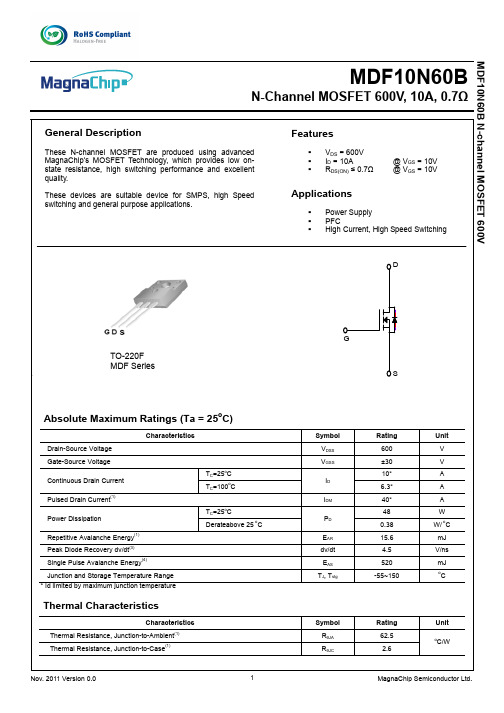
MDF10N60B_datasheet_ver0.0_Nov19_yr11
(1) (1)
Symbol RθJA RθJC
Rating 62.5 2.6
Unit
o
C/W
Nov. 2011 Version 0.0
2.5
BVDSS, (Normalized) Drain-Source Breakdown Voltage
0 50
o
1.1
2.0
1.5
1.0
1.0
0.9
0.5
0.0 -50 100 150
0.8 -50 0 50
o
100
150
TJ, Junction Temperature [ C]
TJ, Junction Temperature [ C]
(1) (1)
Symbol VDSS VGSS TC=25 C TC=100 C
o o
Rating 600 ±30 10*
Unit V V A A A W W/ C mJ V/ns mJ
o o
ID IDM
6.3* 40* 48 0.38 15.6 4.5 520 -55~150
TC=25 C Derateabove 25 C
10
IDR Reverse Drain Current [A]
ID(A)
150℃
1
-55℃
150℃ 25℃
1
25℃
0.1 2 4 6 8
0.1 0.2 0.4 0.6 0.8 1.0 1.2
VGS [V]
VSD, Source-Drain Voltage [V]
APS1006 datasheet_v13_05_08_06

Package/Order Information
Adjustable Output Version:
Fixed Output Versions:
Top View
TOP VIEW
Run 1
5 VFB
GND 2
Top View
TOP VIEW
Run 1
5 VOUT
GND 2
MARKING MARKING
RDS(ON) of P-CH MOSFET ISW = 300mA
0.30 0.50 Ω
RDS(ON) of N-CH MOSFET Peak Inductor Current SW Leakage
ISW = -300mA
VIN=3V, VFB=0.5V or VOUT=90% Duty Cycle <35%
Analog Power Semiconductor
2 of 12
Ver.1.3
APSemi
Electrical Characteristics (Note 5)
(VIN =VRUN= 3.6V, TA = 25°C, Test Circuit Figure 1, unless otherwise noted.)
1
10
100
OUTPUT CURRENT (mA)
1000
Ver.1.3
APSemi
Absolute Maximum Rating (Note 1)
APS1006
Input Supply Voltage ...................... -0.3V to +6V
RUN, VFB Voltages .................. -0.3V to VIN+0.3V SW, Vout Voltages .................. -0.3V to VIN+0.3V Peak SW Sink and Source Current.............. 1.5A
- 1、下载文档前请自行甄别文档内容的完整性,平台不提供额外的编辑、内容补充、找答案等附加服务。
- 2、"仅部分预览"的文档,不可在线预览部分如存在完整性等问题,可反馈申请退款(可完整预览的文档不适用该条件!)。
- 3、如文档侵犯您的权益,请联系客服反馈,我们会尽快为您处理(人工客服工作时间:9:00-18:30)。
对讲机
Module----V1.2
Walkie Talkies 0.5/1W Module----- A1852
DATA SHEET
DATA: 2010-8-4
对讲机
Module----V1.2
一、概述:
A1852是一款性价比极高的全集成对讲机Module,内置高性能射频收发芯片、微控制器以及
射频功放(PA)。外部控制器通过标准的异步串行接口(RS232)设置模块的参数、功能,并可通过
串口AT指令控制整个模块的收发。
该模块体积小、集成度高、性能稳定、应用灵活,且符合世界大多数国家对讲机标准,很容
易通过CE/FCC等认证;采用此模块可做成小型对讲机,也可将模块嵌入到其它手持终端设备以实
现无线对讲功能。
二、特点:
z 宽的工作频率范围:400—470MHz;
z RF输出功率:0.5/1W(可选);
z 低相位噪声和极快的锁相时间(100us);
z 高的频率分辨率,任意频点可调;
z 内建晶体频率温度补偿电路;
z 直接频率综合的调频方式;
z 基于数字信号处理技术的发射滤波器;
z 发射调频增益数字可调;
z 38 CTCSS编解码;
z 高接收灵敏度:-120dBm;
z 全集成接收滤波器;
z 基于数字信号处理技术的调频解调技术
z 超低功耗睡眠模式;
z 异步串口AT指令控制;
z 封装尺寸 :18.9*35.6MM; (模块彩图)
z 3.6~6.0(BAT)电压工作范围;
z 通讯距离:开阔地可达3--5公里
对讲机
Module----V1.2
三、尺寸和脚位(底视图):
J1引脚名称 序号 功能描述
SQ 1 静噪,高电平时控制音频功放静音,可控
制AF_OUT输出与手机音频输出的优先级
别。
NC1 2 NC
AF_OUT 3 音频输出,可根据SQ情况实现静音和对讲
机与手机之间的优先级别。
NC2 4 NC
PTT 5 发射/接收控制脚,1=接收,0=发射
PD 6 模块开关机使能:
PD接地为模块关机,漏电小于30uA;
PD悬空为开机,电流50—65m A
H/L 7 高低功率由AT指令设置
VBAT 8 电源脚
GND1 9 GND
GND2 10 GND
NC5 11 NC
ANT 12 射频输入/输出
NC4 13 NC
NC3 14 NC
对讲机
Module----V1.2
TX LED 15 LED 指示灯,发射时输出高电平
RXD 16 Module接收数据
TXD 17 Module发送数据
MIC_IN 18 MIC输入
四、典型应用电路图:
五 、模块内部框图
A1852
对讲机
Module----V1.2
六、技术参数:
z 直流电气参数(建议工作范围)
符号 描述 最小 典型 最大 单位
VBAT 电源电压 3.6 4.0 4.5 V
Tamp 环境温度 -20 27 60 °C
发送/接收切换时间 20 ms
开电源模块初始化时间 300 500 ms
CMOS低电平电压 0 0.3*VCC V
CMOS高电平电压 0.7*VCC VCC V
z 直流电气参数(最大工作范围)
符号 描述 最小 典型 最大 单位
VBAT 电源电压 3.6 4.2 6.0 V
Tamp 环境温度 -40 90 °C
IIN 输入电流(1) -10 10 mA
VIN 输入电压(1) -0.3 Vcc+0.3 V
MODULE(A1852)
对讲机
Module----V1.2
Notes: 1. 对于以下PIN: SQ, TXD, RXD, PD,PTT,H/L
2. VCC = 3V
z 功耗指标
(测试条件: VBAT = 4.2V , TA = -25 to 55 °C)
工作模式 描述 测试条件 典型值单位
连续接收 接收机正常开启 输入为409.75MHz -47dBm调频信号 60 mA
连续发射 发射机正常开启 输入为1KHz调制信号,高功率: 低功率: 750 450 MA
MA
接收静噪待机 接收机处于工作状态,模块内部语音输出相关模块关断。 55 mA
深睡眠 接收机/发射机均完全关断。 能在300ms内完成上电过程,切换至连续接收/发射模式。 30 uA
z 总体电性能规格说明
频率范围(MHz) 400—470MHz
信道间隔(KHz) 25 / 12.5
天线阻抗(Ω) 50
工作温度范围(℃) -20~+55
频率稳定度(ppm) ±2.0
z 接收特性
(除特别标注外,测试条件为VBAT = 4.0 V, TA = -25 to 55 °C)
符号 参数描述 测试条件 最小典型 最大单位
fIN 射频输入频率范围 对讲机频段 400 470 MHz
对讲机
Module----V1.2
Sensitivity 参考灵敏度 12dB 输出语音信呐比 -119 -120 -122 dBm
静噪开启灵敏度 软件可调 -120
接收信噪比S/N 1.5KHZ频偏 45 50
邻道选择性 12.5KHz信道间隔 55 60 dB
互调抗扰性 12.5KHz信道间隔 55 60
杂散响应抑制 12.5KHz信道间隔 55 60 dB
音频输出阻抗 200 400 Ohm
音频输出幅度 Fo=1KHz 软件可调 1 Vpp
音频输出失真 Fo=1KHz 1 3 %
音频响应 300HZ 500HZ 1KHZ 2500HZ -20 +6 0 -10
接收机本振泄露 LNA端输出 -50 dBm
z 发射特性
(除特别标注外,测试条件为VBAT = 4.0 V, TA = -25 to 55 °C)
符号 参数描述 测试条件 最小典型 最大单位
fOUT 射频输出频率范围 400 470 MHz
POUT 输出功率 H L 700 350 900 450 1100 550 MW
发射电流 H L 700 350 750 400 MA
最大调制频偏限制 窄带 宽带 2.2 4.5 2.5 5.0 KHZ
KHZ
调制灵敏度 1.5KHZ/2.5KHZ频偏(N/W) 8 12 16 MV
音频调制失真 1.5KHZ/2.5KHZ频偏 2 5 %
对讲机
Module----V1.2
(N/W)
调制特性 300HZ 500HZ 1000HZ 2500HZ -5 3 -20 -6 0 6 -9 9 DB
DB
DB
DB
SNR 信噪比 1.5KHZ/2.5KHZ频偏(N/W) 38 40 45 dB
CTCSS调制频偏 0.35 0.5 0.75 KHZ
载波抑制 -60 dBc
IM3 抑制 -60 dBc
邻道功率 12.5KHz offset -60 dBc
杂散辐射 -36 dBc
七、串口通信协议:
A1852模块提供AT指令接口,通过这些DMO AT指令可以方便地跟模块进行通信和控制;该模块
提供的AT指令集涵盖了所有对DMO模块的查询和控制命令,厂家在使用时可根据自身需求,进行挑
选使用,详细请参考《串口通信协议》
(注:模块在没有AT指令时,默认工作参数为:GBW=12.5KHZHZ,TFV=409.75MHZ,
RFV=409.75MHZ,CXCSS=01,SQ=1 ,POWER=0)