LC-RA1212P1, 规格书,Datasheet 资料
VIPer12A功率开关电源IC
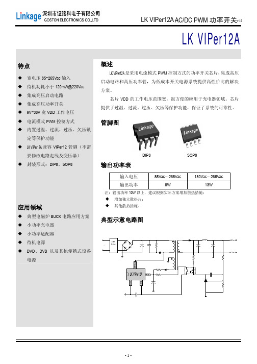
LK VIPer12A AC/DC PWM功率开关v1.6LK VIPer12ADIP8 SOP8输入电压85Vac输出功率10W以上,建议根据实际方案增加散热措施:增加独立散热片;其他散热措施。
LK VIPer12A内部方框图管脚示意图DIP8/SOP8管脚说明名称 管脚序号 管脚说明GND 1,2 芯片地,同时也是内置高压MOS 管SOURCE 端口 FB 3 反馈输入端口VDD 4 芯片电源端,工作电压范围可达9V——38VDRAIN5,6,7,8内置高压MOS 管的DRAIN ,同时芯片启动时,也做芯片的启动LK VIPer12A极限参数极限参数(TA= 25℃)符号说明范围单位V DS(max)芯片DRAIN脚最高耐压-0.3~730 VV DS(ST)芯片启动时,DRAIN脚最高耐压-0.3~400 V VDD 芯片电源电压-0.3~38 VI vdd嵌位电流10 mA I FB最大反馈电流 3 mA V ESD ESD电压>4000 VT J结温-40~150 ℃T STG存储温度-55~150 ℃热阻参数符号说明单位R thJA热阻(1) 45 ℃/W注(1):芯片要焊接在有200mm2铜箔散热的PCB板,铜箔厚度35um,铜箔连接到所有的GND脚。
电气工作参数(除非特殊说明,下列条件均为T A=25℃,VDD=18V)符号说明条件范围单位最小典型最大BV DS漏源击穿电压V FB=2V; I D=1mA 730V - - V I DSS DRAIN端关断态漏电流V FB=2V; V DS=500V - - 0.1 mA R DS(on)源漏端导通电阻I D=0.2A - 19 - Ohm VDD ON VDD开启电压13 14.5 16 V VDD OFF VDD关闭电压7 8 9 V VDD HYS VDD迟滞阈值电压- 6.5 - V VDD OVP VDD过压保护阈值- 39 - V IDD1 VDD工作电流I FB=2.0mA - 0.4 - mA IDD2 VDD工作电流I FB=0.5mA;I D=50mA - 1.0 - mA IDD CH芯片充电电流V DS=100V; VDD=5V - -220 - uA FOSC 芯片振荡频率- 60 - KHz G ID I FB/I DRAIN增益- 320 -I LIMIT峰值电流阈值V FB=0V - 400 - mA I FBSD FB关断电流- 0.9 - mA R FB FB输入电阻I D=0mA - 1.23 - Kohm t LEB前置消隐时间- 300 - ns t ON(min)最小导通时间- 700 - ns t OVT过温保护温度- 150 - ℃t HYS过温迟滞阈值温度- 30 - ℃LK VIPer12A功能表述◆电路图说明上图中D1-D4、C2组成全波整流,D6、R1、C3组成RCD吸收回路,消除变压器T2漏感产生的尖峰电压,避免击穿内部的高压MOS管。
12V2A电源适配器规格书

Vin 115Vac60Hz 输入 115Vac 60Hz
11.7-12.5V ±0.5
V
12.17 11.87 OK
4
Ripple&Noise mVp-p Vin100Vac 60HzFull load
电源适配器 Power adapter
版本/ Version SHEET
OF
K-C7 系列
A1
4
14
3.8 过冲/Overshoot: 在电源开启或关闭的时候,最大 15%. 15% Max.When power supply at turn or turn off.
4、保护功能/PROTECTION FUNCTION:
电源适配器 Power adapter
版本/ Version SHEET
OF
K-C7 系列
A1
8
14
9、铭牌/LABEL:
具体根据客户需求!/ Specific according to customer demand
备注/ Remarks:
1.标签尺寸/ Label size:24.7*27.7mm 2.标签材质/Label Material:黑底白字,光面/Black ground white character,Smooth 3.标签厚度/Label thickness:0.2mm 4.误差/Tolerance:±0.2mm 5 环保/ROHS
额定电压/Rated Voltage:100~240Vac 调整范围/Variation Range:90-264Vac 2.2 输入频率/Input Frequency: 额定频率/ Rated Frequency: 50/60Hz. 调整频率/Variation Frequency:47-63Hz 2.3 输入电流/Input Current: 当输入交流电压为额定值的下限电压负载满载时,最大输入交流电流 1.2A. 1.2Amps max At any input voltage and rated, DC output rated load. 2.4 浪涌电流/Inrush Current: 当输出为额定负载,环境温度为 25℃,输入 240Vac 冷态起机时的最大浪涌电流小于 20A. 20 Amps Max. Cold start at 240Vac input, with rated load and 25℃ ambient. 2.5 AC 漏电流/Ac Leakage Current: 当输入电压 240Vac 时,最大漏电流为 0.25mA. 0.25mA Max.At240Vac input.
NH 熔断器选型手册说明书

NH熔断器选型手册NH- Low voltage H.R.C Fuse西安开尔泰电力电子制造有限公司Xian Kaiert Power Electronics Manufactoring Co.,Ltd.目录TABLE OF CONTENT页码PAGE NH熔断器介绍 3AC NH-400V gG-gL 4-5 AC NH-500V gG-gL 5-7 ACNH-690V gG-gL 7-8 AC NH-500V aM 9AC NH-690V aM 9-10 NH熔断器外形尺寸图10-11 NH熔断器底座外形尺寸图12-14 NH熔断器隔离开关15-19NH 系列低压高分断能力熔断器介绍Product Introduction● 额定电压:400Vac ,500Vac ,690 ac ,1200 Vac ● 额定电流:4A ~1600A ● 七种规格外形尺寸 ● 高分断能力 ● 视觉指示器● 符合GB13539国家低压熔断器标准● 符合IEC60269国际电工低压熔断器标准 ● 符合VDE0636标准第1部分● 符合DIN43620标准第1部分-第4部分NH 高分断低压熔断器按照下列尺寸、电流额定值及运行等级生产:Size 000 2A ~100A Size 00 125A ~160A Size 0 6A ~160A Size 1 80A ~250A Size 2 125A ~400A Size 3250A ~800ASize 4 630A ~1600A Size 4a800A ~1600A本公司生产的NH 系列低压高分断能力熔断器(以下简称NH 熔断器)在吸收国内外同行的产品特点的基础上,在制造工艺、加工设备、检验手段等进行了改进提高,产品性能指标全面符合国际电工委员会标准IEC60269和国家标准GB13539低压熔断器标准。
在国内同行业居领先水平。
本公司生产的NH 熔断器已经广泛用于通讯、电站、开关柜、石油化工、风力发电等行业,获得了用户的一致好评。
CDCLVP1212RHAT;CDCLVP1212RHAR;CDCLVP1212EVM;中文规格书,Datasheet资料

VVV V V V VCDCLVP1212 SCAS886B–AUGUST2009–REVISED AUGUST2011 12LVPECL Output,High-Performance Clock BufferCheck for Samples:CDCLVP1212FEATURES DESCRIPTIONThe CDCLVP1212is a highly versatile,low additive •2:12Differential Bufferjitter buffer that can generate12copies of LVPECL •Selectable Clock Inputs Through Control Pin clock outputs from one of two selectable LVPECL,•Universal Inputs Accept LVPECL,LVDS,and LVDS,or LVCMOS inputs for a variety of LVCMOS/LVTTL communication applications.It has a maximum clockfrequency up to2GHz.The CDCLVP1212features •12LVPECL Outputsan on-chip multiplexer(MUX)for selecting one of two •Maximum Clock Frequency:2GHz inputs that can be easily configured solely through a•Maximum Core Current Consumption:88mA control pin.The overall additive jitter performance isless than0.1ps,RMS from10kHz to20MHz,and •Very Low Additive Jitter:<100fs,rms in10-kHzoverall output skew is as low as25ps,making the to20-MHz Offset Rangedevice a perfect choice for use in demanding • 2.375-V to3.6-V Device Power Supply applications.•Maximum Propagation Delay:550psThe CDCLVP1212clock buffer distributes one of two •Maximum Output Skew:25ps selectable clock inputs(IN0,IN1)to12pairs of •LVPECL Reference Voltage,V AC_REF,Available differential LVPECL clock outputs(OUT0,OUT11)with minimum skew for clock distribution.The for Capacitive-Coupled InputsCDCLVP1212can accept two clock sources into an •Industrial Temperature Range:–40°C to+85°Cinput multiplexer.The inputs can be LVPECL,LVDS,•ESD Protection Exceeds2kV(HBM)or LVCMOS/LVTTL.•Available in6-mm×6-mm QFN-40(RHA)The CDCLVP1212is specifically designed for driving Package50-Ωtransmission lines.When driving the inputs insingle-ended mode,the LVPECL bias voltage APPLICATIONS(VAC_REF)should be applied to the unused negativeinput pin.However,for high-speed performance up to •Wireless Communications2GHz,differential mode is strongly recommended.•Telecommunications/NetworkingThe CDCLVP1212is packaged in a small40-pin,•Medical Imaging6-mm x6-mm QFN package and is characterized for •Test and Measurement Equipment operation from–40°C to+85°C.Please be aware that an important notice concerning availability,standard warranty,and use in critical applications of TexasInstruments semiconductor products and disclaimers thereto appears at the end of this data sheet.All trademarks are the property of their respective owners.PRODUCTION DATA information is current as of publication date.Copyright©2009–2011,Texas Instruments Incorporated Products conform to specifications per the terms of the TexasInstruments standard warranty.Production processing does notnecessarily include testing of all parameters.CDCLVP1212SCAS886B–AUGUST2009–REVISED This integrated circuit can be damaged by ESD.Texas Instruments recommends that all integrated circuits be handled with appropriate precautions.Failure to observe proper handling and installation procedures can cause damage.ESD damage can range from subtle performance degradation to complete device failure.Precision integrated circuits may be more susceptible to damage because very small parametric changes could cause the device not to meet its published specifications.AVAILABLE OPTIONS(1)T A PACKAGED DEVICES FEATURESCDCLVP1212RHAT40-pin QFN(RHA)package,small tape and reel –40°C to+85°CCDCLVP1212RHAR40-pin QFN(RHA)package,tape and reel(1)For the most current specifications and package information,see the Package Option Addendum located at the end of this data sheet orrefer to our web site at .ABSOLUTE MAXIMUM RATINGS(1)Over operating free-air temperature range(unless otherwise noted).CDCLVP1212UNITV CC Supply voltage range(2)–0.5to4.6VV IN Input voltage range(3)–0.5to V CC+0.5VV OUT Output voltage range(3)–0.5to V CC+0.5VI IN Input current20mAI OUT Output current50mAT A Specified free-air temperature range(no airflow)–40to+85°CT STG Storage temperature range–65to+150°CT J Maximum junction temperature+125°CESD Electrostatic discharge(HBM)2kV (1)Stresses beyond those listed under Absolute Maximum Ratings may cause permanent damage to the device.These are stress ratingsonly,and functional operation of the device at these or any other conditions beyond those indicated is not implied.Exposure toabsolute-maximum-rated conditions for extended periods may affect device reliability.(2)All supply voltages must be supplied simultaneously.(3)The input and output negative voltage ratings may be exceeded if the input and output clamp-current ratings are observed. RECOMMENDED OPERATING CONDITIONSOver operating free-air temperature range(unless otherwise noted).CDCLVP1212PARAMETER MIN TYP MAX UNITV CC Supply voltage 2.375 2.50/3.30 3.60VT A Ambient temperature–40+85°C PACKAGE DISSIPATION RATINGS(1)(2)VALUETEST4×4VIASPARAMETER CONDITIONS ON PAD UNIT0LFM36.1°C/WθJA Thermal resistance,junction-to-ambient150LFM30.2°C/W400LFM28.2°C/WθJP(3)Thermal resistance,junction-to-pad 3.58°C/W(1)The package thermal resistance is calculated in accordance with JESD51and JEDEC2S2P(high-K board).(2)Connected to GND with16thermal vias(0.3-mm diameter).(3)θJP(junction-to-pad)is used for the QFN package,because the primary heat flow is from the junction to the GND pad of the QFNpackage.2Submit Documentation Feedback Copyright©2009–2011,Texas Instruments IncorporatedProduct Folder Link(s):CDCLVP1212CDCLVP1212 SCAS886B–AUGUST2009–REVISED AUGUST2011ELECTRICAL CHARACTERISTICS:LVCMOS Input(1)At V CC=2.375V to3.6V and T A=–40°C to+85°C(unless otherwise noted).CDCLVP1212PARAMETER TEST CONDITIONS MIN TYP MAX UNITf IN Input frequency200MHzExternal threshold voltage applied toV th Input threshold voltage 1.1 1.8Vcomplementary inputV IH Input high voltage V th+0.1V CC VV IL Input low voltage0V th–0.1VI IH Input high current V CC=3.6V,V IH=3.6V40μAI IL Input low current V CC=3.6V,V IL=0V–40μAΔV/ΔT Input edge rate20%to80% 1.5V/nsI CAP Input capacitance5pF(1)Figure3and Figure4show dc test setup.ELECTRICAL CHARACTERISTICS:Differential Input(1)At V CC=2.375V to3.6V and T A=–40°C to+85°C(unless otherwise noted).CDCLVP1212PARAMETER TEST CONDITIONS MIN TYP MAX UNITf IN Input frequency Clock input2000MHzf IN≤1.5GHz0.1 1.5VV IN,DIFF,PP Differential input peak-peak voltage1.5GHz≤f IN≤2GHz0.2 1.5VV ICM Input common-mode level 1.0V CC–0.3VI IH Input high current V CC=3.6V,V IH=3.6V40μAI IL Input low current V CC=3.6V,V IL=0V–40μAΔV/ΔT Input edge rate20%to80% 1.5V/nsI CAP Input capacitance5pF(1)Figure5and Figure6show dc test setup.Figure7shows ac test setup.Copyright©2009–2011,Texas Instruments Incorporated Submit Documentation Feedback3Product Folder Link(s):CDCLVP1212CDCLVP1212SCAS886B–AUGUST2009–REVISED ELECTRICAL CHARACTERISTICS:LVPECL Output(1)At V CC=2.375V to2.625V and T A=–40°C to+85°C(unless otherwise noted).CDCLVP1212PARAMETER TEST CONDITIONS MIN TYP MAX UNITV OH Output high voltage V CC–1.26V CC–0.9VV OL Output low voltage V CC–1.7V CC–1.3VV OUT,DIFF,PP Differential output peak-peak voltage f IN≤2GHz0.5 1.35VV AC_REF Input bias voltage(2)I AC_REF=2mA V CC–1.6V CC–1.1VV IN,DIFF,PP=0.1V550pst PD Propagation delayV IN,DIFF,PP=0.3V550pst SK,PP Part-to-part skew150pst SK,O Output skew25psCrossing-point-to-crossing-point distortion,t SK,P Pulse skew(with50%duty cycle input)–5050psf OUT=100MHzf OUT=100MHz,V IN,SE=V CC,V th=1.25V,0.11ps,RMS10kHz to20MHzf OUT=100MHz,V IN,SE=0.9V,0.128ps,RMSV th=1.1V,10kHz to20MHzRandom additive jitter(with50%duty f OUT=2GHz,V IN,DIFF,PP=0.2V,t RJIT0.053ps,RMS cycle input)V ICM=1V,10kHz to20MHzf OUT=100MHz,V IN,DIFF,PP=0.15V,0.093ps,RMSV ICM=1V,10kHz to20MHzf OUT=100MHz,V IN,DIFF,PP=1V,0.092ps,RMSV ICM=1V,10kHz to20MHzt R/t F Output rise/fall time20%to80%200psI EE Supply internal current Outputs unterminated88mAI CC Output and internal supply current All outputs terminated,50Ωto V CC–2468mA(1)Figure8and Figure9show dc and ac test setup.(2)Internally generated bias voltage(V AC_REF)is for3.3-V operation only.It is recommended to apply externally generated bias voltage forV CC<3.0V.4Submit Documentation Feedback Copyright©2009–2011,Texas Instruments IncorporatedProduct Folder Link(s):CDCLVP1212CDCLVP1212 SCAS886B–AUGUST2009–REVISED AUGUST2011ELECTRICAL CHARACTERISTICS:LVPECL Output(1)At V CC=3.0V to3.6V and T A=–40°C to+85°C(unless otherwise noted).CDCLVP1212PARAMETER TEST CONDITIONS MIN TYP MAX UNITV OH Output high voltage V CC–1.26V CC–0.9VV OL Output low voltage V CC–1.7V CC–1.3VV OUT,DIFF,PP Differential output peak-peak voltage f IN≤2GHz0.65 1.35VV AC_REF Input bias voltage I AC_REF=2mA V CC–1.6V CC–1.1VV IN,DIFF,PP=0.1V550pst PD Propagation delayV IN,DIFF,PP=0.3V550pst SK,PP Part-to-part skew150pst SK,O Output skew25psCrossing-point-to-crossing-point distortion,t SK,P Pulse skew(with50%duty cycle input)–5050psf OUT=100MHzf OUT=100MHz,V IN,SE=V CC,V th=1.65V,0.101ps,RMS10kHz to20MHzf OUT=100MHz,V IN,SE=0.9V,0.130ps,RMSV th=1.1V,10kHz to20MHzRandom additive jitter(with50%duty f OUT=2GHz,V IN,DIFF,PP=0.2V,t RJIT0.069ps,RMS cycle input)V ICM=1V,10kHz to20MHzf OUT=100MHz,V IN,DIFF,PP=0.15V,0.094ps,RMSV ICM=1V,10kHz to20MHzf OUT=100MHz,V IN,DIFF,PP=1V,0.094ps,RMSV ICM=1V,10kHz to20MHzt R/t F Output rise/fall time20%to80%200psI EE Supply internal current Outputs unterminated88mAI CC Output and internal supply current All outputs terminated,50Ωto V CC–2468mA(1)Figure8and Figure9show dc and ac test setup.Copyright©2009–2011,Texas Instruments Incorporated Submit Documentation Feedback5Product Folder Link(s):CDCLVP1212CDCLVP1212Thermal Pad(1)12345678910I N _S E LI N P 1I N N 1N CV C CV C CV A C _R E FI N N 0I N P 0OUTN3OUTP3OUTN2OUTP2OUTN1OUTP1OUTN0OUTP0V CCV CC 20191817161514131211O U T P 7O U T P 5G N DO U T P 6O U T P 4O U T N 6O U T N 4O U T N 7O U T N 5G N D 30292827262524232221V CC OUTP8OUTN8OUTP9OUTN9OUTP10OUTN10OUTP11OUTN11V CC31323334353637383940N C CDCLVP1212SCAS886B –AUGUST 2009–REVISED AUGUST 2011PIN CONFIGURATIONRHA PACKAGEQFN-40(TOP VIEW)(1)Thermal pad must be soldered to ground.6Submit Documentation FeedbackCopyright ©2009–2011,Texas Instruments IncorporatedProduct Folder Link(s):CDCLVP1212CDCLVP1212 SCAS886B–AUGUST2009–REVISED AUGUST2011 PIN DESCRIPTIONSCDCLVP1212Pin DescriptionsTERMINAL TERMINAL PULL-UP/NAME NO.TYPE PULLDOWN DESCRIPTION5,6,11,20,V CC Power— 2.5-V/3.3-V supplies for the device31,40GND21,30Ground—Device groundsINP0,INN09,8Input—Differential input pair or single-ended input.Unused input pair can be left floating.Redundant differential input pair or single-ended input.Unused input pair can be INP1,INN12,3Input—left floating.OUTP11,38,39Output—Differential LVPECL output pair no.11.Unused output pair can be left floating.OUTN11OUTP10,36,37Output—Differential LVPECL output pair no.10.Unused output pair can be left floating.OUTN10OUTP9,34,35Output—Differential LVPECL output pair no.9.Unused output pair can be left floating.OUTN9OUTP8,32,33Output—Differential LVPECL output pair no.8.Unused output pair can be left floating.OUTN8OUTP7,28,29Output—Differential LVPECL output pair no.7.Unused output pair can be left floating.OUTN7OUTP6,26,27Output—Differential LVPECL output pair no.6.Unused output pair can be left floating.OUTN6OUTP5,24,25Output—Differential LVPECL output pair no.5.Unused output pair can be left floating.OUTN5OUTP4,22,23Output—Differential LVPECL output pair no.4.Unused output pair can be left floating.OUTN4OUTP3,18,19Output—Differential LVPECL output pair no.3.Unused output pair can be left floating.OUTN3OUTP2,16,17Output—Differential LVPECL output pair no.2.Unused output pair can be left floating.OUTN2OUTP1,14,15Output—Differential LVPECL output pair no.1.Unused output pair can be left floating.OUTN1OUTP012,13Output—Differential LVPECL output pair no.0.Unused output pair can be left floating.OUTN0PulldownIN_SEL1Input MUX select input for input choice(see Table2)(see Table1)Bias voltage output for capacitive coupled inputs.Do not use V AC_REF at V CC< V AC_REF7Output— 3.0V.If used,it is recommended to use a0.1-μF capacitor to GND on this pin.The output current is limited to2mA.NC4,10——Do not connectTable1.Pin CharacteristicsPARAMETER MIN TYP MAX UNITSR PULLDOWN Input pulldown resistor150kΩTable2.Input Selection TableIN_SEL ACTIVE CLOCK INPUT0INP0,INN01INP1,INN1Copyright©2009–2011,Texas Instruments Incorporated Submit Documentation Feedback7Product Folder Link(s):CDCLVP12120.20.40.60.81.01.21.41.62.01.8Frequency (GHz)1.00.90.80.70.60.50.4D i f f e r e n t i a l O u t p u t P e a k -t o -P e a k V o l t a g e (V)0.20.40.60.81.01.21.41.62.01.8Frequency (GHz)1.11.21.31.00.90.80.70.60.50.4D i f f e r e n t i a l O u t p u t P e a k -t o -P e a k V o l t a g e (V )CDCLVP1212SCAS886B –AUGUST 2009–REVISED AUGUST 2011TYPICAL CHARACTERISTICSAt T A =–40°C to +85°C (unless otherwise noted).DIFFERENTIAL OUTPUT PEAK-TO-PEAK VOLTAGEvs FREQUENCYFigure 1.DIFFERENTIAL OUTPUT PEAK-TO-PEAK VOLTAGEvs FREQUENCYFigure 2.8Submit Documentation FeedbackCopyright ©2009–2011,Texas Instruments IncorporatedProduct Folder Link(s):CDCLVP1212VV V thV IHmaxV ILmaxV IHminV ILminV IHV ILV th V V V GNDV CCV V CDCLVP1212SCAS886B –AUGUST 2009–REVISED AUGUST 2011TEST CONFIGURATIONSThis section describes the function of each block for the CDCLVP1212.Figure 3through Figure 9illustrate how the device should be set up for a variety of test configurations.Figure 3.DC-Coupled LVCMOS Input During Device TestFigure 4.V th Variation over LVCMOS LevelsFigure 5.DC-Coupled LVPECL Input During Device TestCopyright ©2009–2011,Texas Instruments Incorporated Submit Documentation Feedback9Product Folder Link(s):CDCLVP1212CDCLVP1212SCAS886B–AUGUST2009–REVISED Figure6.DC-Coupled LVDS Input During Device TestV VFigure7.AC-Coupled Differential Input to DeviceFigure8.LVPECL Output DC Configuration During Device TestFigure9.LVPECL Output AC Configuration During Device Test10Submit Documentation Feedback Copyright©2009–2011,Texas Instruments IncorporatedProduct Folder Link(s):CDCLVP1212分销商库存信息:TICDCLVP1212RHAT CDCLVP1212RHAR CDCLVP1212EVM。
ROM-0505S;ROM-1212S;ROM-0512S;ROM-1205S;ROM-0515S;中文规格书,Datasheet资料

Selection GuidePart Input Output Output Efficiency Max.NumberVoltage Voltage Current Capacitive SIP4 Micro Size Pack.(VDC)(VDC)(mA)(%)Load (1)ROM-xx05S 3.3, 5, 12520070-781000µF ROM-xx12S3.3, 5, 12128378-82470µF ROM-xx15S 3.3, 5, 12156680-84470µFxx = Input Voltage (other input and output voltage combinations available on request)* add Suffix “P” for Continuous Short Circuit Protection, e.g. ROM-0505S/PO u t p u t P o w e r (%)100602040Operating Temperature °C80Specifications (measured at T A = 25°C, nominal input voltage, full load and after warm-up)1 WattSIP4 Micro Single OutputDerating-Graph(Ambient T emperature)●Micro Size SIP4 Package ●3kVDC Isolation●Approved for Medical Applications ●Industry Standard Pinout●Optional Continuous Short Circuit Protected ●UL94V-0 Package Material ●Efficiency to 85%FeaturesUnregulated ConvertersInput Voltage Range ±10%Output Voltage Accuracy ±5%Line Voltage Regulation 1.2%/1% of Vin typ.Load Voltage Regulation 5V Output 15% max.(10% to 100% full load)12V, 15V Output10% max.Output Ripple and Noise (20MHz limited)100mVp-p max.Operating Frequency 50kHz min. / 100kHz typ. / 105kHz max.Efficiency at Full Load 70% min. / 80% typ.Minimum Load = 0%Specifications valid for 10% minimum load only.Isolation Voltage (tested for 1 second)3000VDC (rated for 1 minute)1500VAC / 60Hz Isolation Capacitance 20pF min. / 75pF max.Isolation Resistance 15 G Ωmin.Short Circuit Protection 1 Second P-SuffixContinuousOperating Temperature Range (free air convection)-40°C to +85°C (see Graph)Storage Temperature Range -55°C to +125°CRelative Humidity 95% RHPackage Weight 1gPacking Quantity 42 pcs per TubeMTBF (+25°C)using MIL-HDBK 217F 977 x 103 hours (+85°C)using MIL-HDBK 217F189 x 103 hoursThe ROM Micro Size DC/DC converter has been designed for isolating or converting DC power rails where board height is at a premium. Although it has a micro-size 7.7mm package, it does not compromise on features and offers a high 3kVDC Isolation , a –40°C to +85°C operating temperature range and optional continuous short circuit protection.Description}Detailed Information seeApplication Notes chapter "MTBF"EN-60950-1 Certified UL-60950-1 Certified EN-60601-1 CertifiedREV:1/2011E-17 ECONOLINEDC/DC-Converterwith 3 year WarrantyRefer to Application NotesRoHS2002/95/EC6/6E-224736ROM/E-18REV: 1/2011R O MPackage Style and Pinning (mm)3rd angle projectionRecommended Footprint Details4 PIN SIP Micro Size PackageXX.X ± 0.5 mm XX.XX ± 0.25 mmRO Pin Connections Pin #Single1 –Vin2 +Vin3 –Vout4+VoutTypical CharacteristicsROM SeriesECONOLINEDC/DC-ConverterE f f i c i e n c y %100040%0%100%40Efficiency / Load60%80%20%206080Total Output current (%)Deviation / Load-10.00040%0%100%D e v i a t i o n f r o m N o m in a l (%)60%80%20%-5.000Total Output current (%)0.0005.00010.00015.00020.00025.000E f f i c i e n c y %100040%0%100%40Efficiency / Load 60%80%20%206080Total Output current (%)E f f i c i e n c y %10040%0%100%40Efficiency / Load 60%80%20%206080Total Output current (%)Deviation / Load-10.00040%0%100%D e v i a t i o n f r o m N o m i n a l (%)60%80%20%-5.000Total Output current (%)0.0005.00010.00015.00020.00025.000Deviation / Load-10.00040%0%100%D e v i a t i o n f r o m N o m i n a l (%)60%80%20%-5.000Total Output current (%)0.0005.00010.00015.00020.00025.000ROM-xx05SROM-xx15SROM-xx12SNotes Note 1Maximum capacitive load is defined as the capacitive load that will allow start up in under 1 second without damage to the converter.Certifications CB Test Report Report: US/15348/UL IEC 60950-1:2005 2nd Ed.UL General Safety Report: E224736UL 60950-1 1st Ed.EN General Safety Report: PS080804950C2EN60950-1:2001 + A11:2004EN Medical safetyReport: ETS-0600068AEN 60601-1/分销商库存信息:RECOM-POWERROM-0505S ROM-1212S ROM-0512S ROM-1205S ROM-0515S ROM-1215S ROM-0512S/P ROM-0515S/P ROM-1205S/P ROM-1212S/P ROM-1215S/P ROM-0505S/P。
LP12A规格书
图4. (1)上电 (2)正常工作 (3)自动重启 (4)电源关断时的典型波形
脉宽调制器 脉宽调制器通过驱动输出MOSFET来实现多模式控制,其占空比与流入控制脚超过芯片内部消 耗所需要的电流成反比(如图3)。反馈误差信号以过电流的形式, 由一个典型转折频率为 7 kHz的RC滤波电路进行滤波,以降低芯片电源电流中由MOSFET栅极驱动产生的开关噪音。 要优化电源效率,需要实施四个不同的控制模式。在最大负载条件下,调制器将在全频PWM 模式下进行工作,随着负载的增加,调制器将自动依次切换到变频PWM模式和低频PWM模式。 在轻负载条件下,控制方式将从PWM控制切换到多周期调制控制,调制器在多周期调制模式 下进行工作。虽然不同模式的工作方式有所不同,但为了实现模式间的平滑切换,图3中所
振荡器和开关频率 内部振荡器使内部电容在两个设定的电压值间线性充放电,以产生脉宽调制解调器所需的三 角波电压。在每个周期的起点,振荡器将脉宽调制解调器/电流限制的触发器电路置位。全 开关频率选择为66kHz。全频PWM模式下,66kHz开关频率大约在±2.5kHz的范围内以250Hz 的速率抖动。当系统进入固定漏极峰值电流的变频模式后,频率抖动将关闭。
图 2. 内部结构框图
引脚功能描述
管脚 1
5,6,7,8 3 4 2
符号 S D C NC M
管脚定义描述 功率管的源极 功率管的漏极 控制反馈引脚 空脚,不连接 多功能引脚
控制(C)引脚: 误差放大器及反馈电流的输入脚,用于占空比控制。与内部并联调整器相连接,提供正常工 作时的内部偏置电流。也用作电源旁路和自动重启动/补偿电容的连接点。 漏极(D)引脚: 高压功率MOSFET漏极引脚。通过内部的开关高压电流源提供启动偏置电流。 源极(S)引脚: 这个引脚是功率MOSFET的源极连接点,用于高压功率的回路。它也是控制反馈脚的参考地。 空脚(NC)引脚: 该脚为空脚,与芯片内部无连接,外部应用无需连接。 多功能(M)引脚: 是过压(OV)、欠压(UV)、降低DCMAX的线电压前馈、输出过压保护(OVP)、外部流限调节、远 程开/关和器件重置的输入引脚。多功能引脚组合了电压监测及外部流限引脚功能。但其中 某些功能不能同时实现。连接至源极则禁用此引脚的所有功能实现简单的三端模式工作。
1212外形尺寸电感

能 够 以 M 有 的 高 集 成 性 与 易 用 性 源 电 压 和 纹 波 噪 声 不 敏 感 , 对 环 境 光 具 锁 。 在 XL系 列 中 , 目前 可 提 供 2 触 点 CU固 9 实 现性 能平 衡 。
Te s n t u n s 源自a Is r me t 有 更 好 的 抵 御 能 力 。 器件 的 环 氧 树 脂 透 型 号 ,可 用 于 组 装 0 2 m厚 的FPC电 .m 镜盖被设计成红外滤波器。
1 1J 形尺寸 电感 22b  ̄
I L P一 1 A B一 11 I Lp- H 2 2l 和 H
款采用科锐最新Die t t c L D 在 3 kH ~5 kH z 载 波 频 率 下 。 这 r c Ata h E 6 Z 6 的
技术的高功率L ED。直 接 贴 装 ( r c 些 器 件 的 传 输 距 离 为 3 i 并 与 市 场 1 l A E l 采 用 1 1 N 装 的 电 感 , Die t 2 2 一1 是 22 5n, Atah)技 术 是 科 锐 独 有 的 新 一 代L D tc E 上 的 标 准 产 品 管 脚 兼 容 。所 有 器 件 分 别 具 有 1 2 m和 1 5 m 的 超 低 厚 .m .m 芯 片技 术 ,可 提 供 更 高 的 亮 度 、 更 低 的 均 符 合 RO S 0 2 9 / W EEE 度 。 I LP 1 A B一1 和 I LP H —l 22 1 H 一 H 2 0 / 5 EC和
一
DC D C / 转换 器应用 、高 电流电源和 负 载点转换器、分布式 电源 系统等。
I P 2 2 l 的感值范 围为 HL 一1 1AB 1
0 2 ~0 5 H,饱和 电流 范 围为6 7 . 2 .6 .
AFB1212HHE;中文规格书,Datasheet资料
Descriptions:1. Delta will not guarantee the performance of the products if the application condition fallsoutside the parameters set forth in the specification.2. A written request should be submitted to Delta prior to approval if deviation from thisspecification is required.3. Please exercise caution when handling fans. Damage may be caused when pressure is appliedto the impeller, if the fans are handled by the lead wires, or if the fans are hard-dropped to the production floor.4. Except as pertains to some special designs, there is no guarantee that the products will be freefrom any such safety problems or failures as caused by the introduction of powder, droplets of water or encroachment of insect into the hub.5. The above-mentioned conditions are representative of some unique examples and viewed as thefirst point of reference prior to all other information.6. It is very important to establish the correct polarity before connecting the fan to the powersource. Positive (+) and Negative (-). Damage may be caused to the fans if connection is with reverse polarity, as there is no foolproof method to protect against such error.7. Delta fans are not suitable where any corrosive fluids are introduced to their environment.8. Please ensure all fans are stored according to the storage temperature limits specified. Do notstore fans in a high humidity environment. We highly recommend performance testing is conducted before shipping, if the fans have been stored over 6 months.9. Not all fans are provided with the Lock Rotor Protection feature. If you impair the rotation ofthe impeller for the fans that do not have this function, the performance of those fans will lead to failure.10. Please be cautious when mounting the fan. Incorrect mounting of fans may cause excessresonance, vibration and subsequent noise.11. It is important to consider safety when testing the fans. A suitable fan guard should be fitted tothe fan to guard against any potential for personal injury.12. Except where specifically stated, all tests are carried out at relative (ambient) temperature andhumidity conditions of 25o C, 65%. The test value is only for fan performance itself.13. Be certain to connect an “over 4.7µF” capacitor to the fan externally when the application callsfor using multiple fans in parallel, to avoid any unstable power.分销商库存信息: DELTA-PRODUCT-GROUPS AFB1212HHE。
- 1、下载文档前请自行甄别文档内容的完整性,平台不提供额外的编辑、内容补充、找答案等附加服务。
- 2、"仅部分预览"的文档,不可在线预览部分如存在完整性等问题,可反馈申请退款(可完整预览的文档不适用该条件!)。
- 3、如文档侵犯您的权益,请联系客服反馈,我们会尽快为您处理(人工客服工作时间:9:00-18:30)。
2
4
6 8 10
20
40
(Minute)
(Hour)
Duration of discharge
Duration of discharge vs. Discharge current
30 20 15 10
(Note)
Internal Resistance Temperature dependency of capacity (20 hour rate) Self discharge 77˚F (25˚C)
(mA)
(A) Discharge current
VRLA BATTERIES芯天ຫໍສະໝຸດ --/AUGUST 2005
This information is generally descriptive only and is not intended to make or imply any representation, guarantee or warranty with respect to any cells and batteries. Cell and battery designs/specifications are subject to modification without notice. Contact Panasonic for the latest information.
0.394 + 0.039 (10 +1.0 )
Photo/Label for reference only.
Nominal Voltage Rated Capacity (20 hour rate) Length Dimensions Width Height Total Height* Approx. mass
12A 24A
20 40 60
6A
3A
1.2A 0.6A
Characteristics
Capacity (note) 77˚F (25˚C) 20 hour rate (600mA) 10 hour rate (1130mA) 5 hour rate (2080mA) 1 hour rate (8100mA) 1.5 hour rate discharge Cut-off voltage 10.5 V Fully charged battery 77˚F (25˚C) 104˚F (40˚C) 77˚F (25˚C) 32˚F (0˚C) 5˚F (-15˚C) Residual capacity after standing 3 months Residual capacity after standing 6 months Residual capacity after standing 12 months Initial current Control voltage Initial current Trickle use Control voltage 12Ah 11.3Ah 10.4Ah 8.1Ah 5.8A Approx. 30mΩ 102% 100% 85% 65% 91% 82% 64% 4.8 A or smaller 14.5V to 14.9V (per 12V cell 25˚C) 1.8 A or smaller 13.6V to 13.8V (per 12V cell 25˚C)
VALVE-REGULATED LEAD ACID BATTERIES: INDIVIDUAL DATA SHEET
LC-RA1212P
For main and standby power supplies. Expected trickle life: 3-5 years at 25°C, Approx. 5 years at 20°C.
0 1 2 4 6 8 10
3.937 inches (100.0 mm)
UL94HB Faston 187 UL94HB Faston 250
0.012 (0.3)
Specifications
3.701- 0.020 (94 + 1.5 ) - 0.5
+ 0.059
* The total height with #250 teminal is 101.5mm.
20
10
(Note) The above characteristics data are average values obtained within three charge/discharge. Cycles not the minimum values.
300 500
1
3
5
10
30
50
100
Dimensions (mm)
Terminal type: Faston 187 or Faston 250
0.236 (6)
0.534±0.3 (13.5±0.75)
5.945 + 0.059 - 0.020 151 + 1.5 - 0.5
3.858 + 0.059 - 0.020 (98 + 1.5 ) - 0.5
Standard Terminals and Resin
12V 12Ah 5.945 inches (151.0 mm) 3.860 inches (98.0 mm) 3.702 inches (94.0 mm) 8.36 lbs. (3.8 kg) LC-RA1212P LC-RA1212P1
Terminal voltage (V)
(Hour)
Duration of discharge
5 4 3 2 1.5 1 50 40 30
104˚F (40˚C)
77˚F (25˚C)
32˚F (0˚C)
5˚F (-15˚C)
(Minute)
Charge Method (Constant Voltage)
Cycle use (Repeating use)
Battery case resin: Standard (UL94HB) Color is black.
Discharge characteristics 77°F (25°C) (Note)
14.4 13.8 13.2 12.6 12.0 11.4 10.8 10.2 9.6 9.0 8.4 7.8