P4SMAJ26C中文资料
卡萨帝家用变频空调 KFR-26GW_03ACQ22AK说明书

KFR-26GW/03AAQ22AK(吉尔特白)KFR-35GW/03AAQ22AK(吉尔特白)家用变频空调KFR-26GW/03AAQ22AK(吉尔特黑)KFR-35GW/03AAQ22AK(吉尔特黑)KFR-26GW/03ABQ22AK KFR-35GW/03ABQ22AK KFR-26GW/03ACQ22AK KFR-35GW/03ACQ22AK1卡萨帝为了精确实现您的格调生活,对其家族每一类产品都赋予了专属的境界理念。
本产品为您带来的是冷暖随适。
2关于本产品的安全注意事项.........................................................3本产品的安装事项 (5)安装注意事项.......................................................................5随机附件..............................................................................5电力要求..............................................................................5室内外机安装图...................................................................6安装(按照室内机组安装图进行安装).................................6管路系统图...........................................................................6安装检查及试运转................................................................7室内机管路布置...................................................................7接线方法..............................................................................8室内外机接线.......................................................................8排空方法(R410A )..............................................................9本产品的外观及部件介绍...........................................................10室内机................................................................................10室内机显示面板.................................................................10室外机................................................................................10遥控器.................................................................................11本产品的主要功能介绍 (12)1.遥控器的使用..............................................................122.智能/省电/查询/温度显示功能...............................123.停电补偿功能..............................................................134.制冷/制热/除湿/送风/自动....................................145.调节风向.....................................................................146.除甲醛功能/水离子功能............................................157.静眠功能.....................................................................168.应急运转/试验运转....................................................1610.强力/安静功能...........................................................1711.定时开-关功能...........................................................17本产品的日常保养与维护.. (18)空气过滤网及除甲醛模块的安装........................................18清洗机器............................................................................18换季收存............................................................................18有疑问?先看这儿! (19)(若对空调有疑问,请先按本章内容检查处理。
AM26LS31C_08中文资料

FEATURESDESCRIPTION/ORDERING INFORMATIOND, DB, N, NS, J, OR W PACKAGE(TOP VIEW)Y A C AGN N332FK PACKAGE(TOP VIEW)CCAM26LS31C,AM26LS31M QUADRUPLE DIFFERENTIAL LINE DRIVER SLLS114I–JANUARY1979–REVISED FEBRUARY2006•Meets or Exceeds the Requirements of ANSITIA/EIA-422-B and ITU•Operates From a Single5-V Supply•TTL Compatible•Complementary Outputs•High Output Impedance in Power-OffConditions•Complementary Output-Enable InputsThe AM26LS31is a quadruple complementary-outputline driver designed to meet the requirements of ANSITIA/EIA-422-B and ITU(formerly CCITT)Recommendation V.11.The3-state outputs havehigh-current capability for driving balanced lines suchas twisted-pair or parallel-wire transmission lines,andthey are in the high-impedance state in the power-offcondition.The enable function is common to all fourdrivers and offers the choice of an active-high oractive-low enable(G,G)input.Low-power Schottkycircuitry reduces power consumption withoutsacrificing speed.ORDERING INFORMATIONT A PACKAGE(1)ORDERABLE PART NUMBER TOP-SIDE MARKING PDIP–N Tube AM26LS31CN AM26LS31CNTube AM26LS31CDSOIC–D AM26LS31C0°C to70°C Tape and reel AM26LS31CDRSOP–NS Tape and reel AM26LS31CNSR26LS31SSOP–DB Tape and reel AM26LS31CDBR SA31CCDIP–J Tube AM26LS31MJB AM26LS31MJB–55°C to125°C LCCC–FK Tube AM26LS31MFKB AM26LS31MFKB CFP–W Tube AM26LS31MWB AM26LS31MWB(1)Package drawings,standard packing quantities,thermal data,symbolization,and PCB design guidelines are available at/sc/package.Please be aware that an important notice concerning availability,standard warranty,and use in critical applications of Texas Instruments semiconductor products and disclaimers thereto appears at the end of this data sheet.1Z 1Y G G 1A2Z 2Y 2A3Z 3Y 3A4Z4Y 4AAM26LS31C,AM26LS31MQUADRUPLE DIFFERENTIAL LINE DRIVERSLLS114I–JANUARY 1979–REVISED FEBRUARY 2006FUNCTION TABLE (1)(EACH DRIVER)ENABLES OUTPUTS INPUT A G G Y Z H H X H L L H X L H H X L H L L X L L H X LHZZ(1)H =high level,L =low level,X =irrelevant,Z =high impedance (off)LOGIC DIAGRAM (POSITIVE LOGIC)All resistor values are nominal.Absolute Maximum Ratings (1)AM26LS31C,AM26LS31MQUADRUPLE DIFFERENTIAL LINE DRIVERSLLS114I–JANUARY 1979–REVISED FEBRUARY 2006SCHEMATIC (EACH DRIVER)over operating free-air temperature range (unless otherwise noted)MINMAXUNIT V CC Supply voltage (2)7V V IInput voltage7V Output off-state voltage5.5VD package73DB package 82θJAPackage thermal impedance (3)°C/W N package 67NS package64Lead temperature 1,6mm (1/16in)from case for 10s 260°C Lead temperature 1,6mm (1/16in)from case for 60sJ package300°C T stg Storage temperature range–65150°C (1)Stresses beyond those listed under "absolute maximum ratings"may cause permanent damage to the device.These are stress ratings only,and functional operation of the device at these or any other conditions beyond those indicated under "recommended operating conditions"is not implied.Exposure to absolute-maximum-rated conditions for extended periods may affect device reliability.(2)All voltage values,except differential output voltage V OD ,are with respect to network GND.(3)The package thermal impedance is calculated in accordance with JESD 51-7.Recommended Operating ConditionsElectrical Characteristics (1)Switching CharacteristicsAM26LS31C,AM26LS31MQUADRUPLE DIFFERENTIAL LINE DRIVERSLLS114I–JANUARY 1979–REVISED FEBRUARY 2006MINNOMMAX UNIT AM26LS31C 4.755 5.25V CC Supply voltage V AM26LS31M4.555.5V IH High-level input voltage 2V V IL Low-level input voltage 0.8V I OH High-level output current –20mA I OL Low-level output current 20mA AM26LS31C 070T AOperating free-air temperature°CAM26LS31M–55125over operating free-air temperature range (unless otherwise noted)PARAMETERTEST CONDITIONSMINTYP (2)MAX UNIT V IK Input clamp voltage V CC =MIN,I I =–18mA –1.5V V OH High-level output voltage V CC =MIN,I OH =–20mA 2.5V V OL Low-level output voltage V CC =MIN,I OL =20mA 0.5V V O =0.5V –20Off-state (high-impedance-state)I OZ V CC =MIN,µA output currentV O =2.5V 20I I Input current at maximum input voltage V CC =MAX,V I =7V 0.1mA I IH High-level input current V CC =MAX,V I =2.7V 20µA I IL Low-level input current V CC =MAX,V I =0.4V–0.36mA I OS Short-circuit output current (3)V CC =MAX –30–150mA I CC Supply currentV CC =MAX,All outputs disabled3280mA(1)For C-suffix devices,V CC min =4.75V and V CC max =5.25V.For M-suffix devices,V CC min =4.5V and V CC max =5.5V.(2)All typical values are at V CC =5V and T A =25°C.(3)Not more than one output should be shorted at a time,and duration of the short circuit should not exceed one second.V CC =5V (see Figure 1)T A =25°C AM26LS31M PARAMETERTEST CONDITIONSUNITMINTYP MAX MINMAX Propagation delay time,low-to t PLH 142030high-level outputC L =30pF,S1and S2openns Propagation delay time,high-to t PHL 142030low-level outputt PZH Output enable time to high level R L =75Ω254060C L =30pF ns t PZL Output enable time to low level R L =180Ω374568t PHZ Output disable time from high level 213045C L =10pF,S1and S2closed ns t PLZ Output disable time from low level 233553t SKEWOutput-to-output skewC L =30pF,S1and S2open169nsPARAMETER MEASUREMENT INFORMATIONWaveform 1 (see Note E)Output ZOutput YInput A(see Notes Band C)V OLV OHV OLV OH3 Vt PHLSkew Skewt PLHt PLHt PHL0 VPROPAGATION DELAY TIMES AND SKEW TEST CIRCUITVTest Point180 ΩFrom OutputUnder TestV OHV OL≈1.5 V0 V3 VEnable GEnable G(see Note D)S1 OpenS2 ClosedS1 ClosedS2 Opent PZHt PZLt PHZt PLZS1 ClosedS2 Closed0.5 V≈0 V≈4.5 VS1 ClosedS2 Closed≈1.5 VENABLE AND DISABLE TIME WAVEFORMSSee Note DNOTES: A.C L includes probe and jig capacitance.B.All input pulses are supplied by generators having the following characteristics: PRR ≤ 1 MHz, Z O≈ 50 Ω, t r≤ 15 ns, t f≤ 6 ns.C.When measuring propagation delay times and skew, switches S1 and S2 are open.D.Each enable is tested separately.E.Waveform 1 is for an output with internal conditions such that the output is low, except when disabled by the output control.Waveform 2 is for an output with internal conditions such that the output is high, except when disabled by the output control.1.3 V 1.3 V1.5 V1.5 V1.5 V 1.5 VWaveform 2(see Note E)0.5 V1.5 V1.5 VAM26LS31C,AM26LS31MQUADRUPLE DIFFERENTIAL LINE DRIVERSLLS114I–JANUARY1979–REVISED FEBRUARY2006Figure1.Test Circuit and Voltage WaveformsTYPICAL CHARACTERISTICSV I − Enable G Input Voltage − VOUTPUT VOLTAGEvsENABLE G INPUT VOLTAGE− Y O u t p u t V o l t a g e − VV O 43210V I − Enable G Input Voltage − VOUTPUT VOLTAGEvsENABLE G INPUT VOLTAGE− Y O u t p u t V o l t a g e − VV O V I − Enable G Input Voltage − V − O u t p u t V o l t a g e − VOUTPUT VOLTAGEvsENABLE G INPUT VOLTAGEVO 4321056V I − Enable G Input Voltage − VOUTPUT VOLTAGEvsENABLE G INPUT VOLTAGE− O u t p u t V o l t a g e − VV O 43210012356AM26LS31C,AM26LS31MQUADRUPLE DIFFERENTIAL LINE DRIVERSLLS114I–JANUARY 1979–REVISED FEBRUARY 2006Figure 2.Figure 3.Figure 4.Figure 5.A.The A input is connected to V CC during testing of the Y outputs and to ground during testing of the Z outputs.B.The A input is connected to ground during testing of the Y outputs and to V CC during testing of the Z outputs.− H i g h -L e v e l O u t p u t V o l t a g e − VT A − Free-Air Temperature − °CHIGH-LEVEL OUTPUT VOLTAGEvsFREE-AIR TEMPERATUREV O H 432105I OH − High-Level Output Current − mAHIGH-LEVEL OUTPUT VOLTAGEvsHIGH-LEVEL OUTPUT CURRENT− H i g h -L e v e l O u t p u t V o l t a ge − VV O H 43210− L o w -L e v e l O u t p u t V o l t a g e − VT A − Free-Air Temperature − °CLOW-LEVEL OUTPUT VOLTAGEvsFREE-AIR TEMPERATUREV O L I OL − Low-Level Output Current − mALOW-LEVEL OUTPUT VOLTAGEvsLOW-LEVEL OUTPUT CURRENT− L o w -L e v e l O u t p u t V o l t a g e − VV O L 0.40.30.20.100.50.60.70.80.91AM26LS31C,AM26LS31MQUADRUPLE DIFFERENTIAL LINE DRIVERSLLS114I–JANUARY 1979–REVISED FEBRUARY 2006TYPICAL CHARACTERISTICS (continued)Figure 6.Figure 7.Figure 8.Figure 9.A.The A input is connected to V CC during testing of the Y outputs and to ground during testing of the Z outputs.B.The A input is connected to ground during testing of the Y outputs and to V CC during testing of the Z outputs.V I − Data Input Voltage − VY OUTPUT VOLTAGEvsDATA INPUT VOLTAGE− Y O u t p u t V o l t a g e − VV O 432105Y OUTPUT VOLTAGEvsDATA INPUT VOLTAGEV I − Data Input Voltage − V− Y O u t p u t V o l t a g e − VV O 0123AM26LS31C,AM26LS31MQUADRUPLE DIFFERENTIAL LINE DRIVERSLLS114I–JANUARY 1979–REVISED FEBRUARY 2006TYPICAL CHARACTERISTICS (continued)Figure 10.Figure 11.PACKAGING INFORMATIONOrderable Device Status(1)PackageType PackageDrawingPins PackageQtyEco Plan(2)Lead/Ball Finish MSL Peak Temp(3)5962-7802301M2A ACTIVE LCCC FK201TBD POST-PLATE N/A for Pkg Type 5962-7802301MEA ACTIVE CDIP J161TBD A42SNPB N/A for Pkg Type 5962-7802301MFA ACTIVE CFP W161TBD A42SNPB N/A for Pkg Type AM26LS31CD ACTIVE SOIC D1640Green(RoHS&no Sb/Br)CU NIPDAU Level-1-260C-UNLIMAM26LS31CDBR ACTIVE SSOP DB162000Green(RoHS&no Sb/Br)CU NIPDAU Level-1-260C-UNLIMAM26LS31CDBRE4ACTIVE SSOP DB162000Green(RoHS&no Sb/Br)CU NIPDAU Level-1-260C-UNLIMAM26LS31CDBRG4ACTIVE SSOP DB162000Green(RoHS&no Sb/Br)CU NIPDAU Level-1-260C-UNLIMAM26LS31CDE4ACTIVE SOIC D1640Green(RoHS&no Sb/Br)CU NIPDAU Level-1-260C-UNLIMAM26LS31CDG4ACTIVE SOIC D1640Green(RoHS&no Sb/Br)CU NIPDAU Level-1-260C-UNLIMAM26LS31CDR ACTIVE SOIC D162500Green(RoHS&no Sb/Br)CU NIPDAU Level-1-260C-UNLIMAM26LS31CDRE4ACTIVE SOIC D162500Green(RoHS&no Sb/Br)CU NIPDAU Level-1-260C-UNLIMAM26LS31CDRG4ACTIVE SOIC D162500Green(RoHS&no Sb/Br)CU NIPDAU Level-1-260C-UNLIMAM26LS31CN ACTIVE PDIP N1625Pb-Free(RoHS)CU NIPDAU N/A for Pkg TypeAM26LS31CNE4ACTIVE PDIP N1625Pb-Free(RoHS)CU NIPDAU N/A for Pkg TypeAM26LS31CNSR ACTIVE SO NS162000Green(RoHS&no Sb/Br)CU NIPDAU Level-1-260C-UNLIMAM26LS31CNSRG4ACTIVE SO NS162000Green(RoHS&no Sb/Br)CU NIPDAU Level-1-260C-UNLIM AM26LS31MFKB ACTIVE LCCC FK201TBD POST-PLATE N/A for Pkg Type AM26LS31MJB ACTIVE CDIP J161TBD A42SNPB N/A for Pkg Type AM26LS31MWB ACTIVE CFP W161TBD A42SNPB N/A for Pkg Type (1)The marketing status values are defined as follows:ACTIVE:Product device recommended for new designs.LIFEBUY:TI has announced that the device will be discontinued,and a lifetime-buy period is in effect.NRND:Not recommended for new designs.Device is in production to support existing customers,but TI does not recommend using this part in a new design.PREVIEW:Device has been announced but is not in production.Samples may or may not be available.OBSOLETE:TI has discontinued the production of the device.(2)Eco Plan-The planned eco-friendly classification:Pb-Free(RoHS),Pb-Free(RoHS Exempt),or Green(RoHS&no Sb/Br)-please check /productcontent for the latest availability information and additional product content details.TBD:The Pb-Free/Green conversion plan has not been defined.Pb-Free(RoHS):TI's terms"Lead-Free"or"Pb-Free"mean semiconductor products that are compatible with the current RoHS requirements for all6substances,including the requirement that lead not exceed0.1%by weight in homogeneous materials.Where designed to be soldered at high temperatures,TI Pb-Free products are suitable for use in specified lead-free processes.Pb-Free(RoHS Exempt):This component has a RoHS exemption for either1)lead-based flip-chip solder bumps used between the die and package,or2)lead-based die adhesive used between the die and leadframe.The component is otherwise considered Pb-Free(RoHS compatible)as defined above.Green(RoHS&no Sb/Br):TI defines"Green"to mean Pb-Free(RoHS compatible),and free of Bromine(Br)and Antimony(Sb)based flame retardants(Br or Sb do not exceed0.1%by weight in homogeneous material)(3)MSL,Peak Temp.--The Moisture Sensitivity Level rating according to the JEDEC industry standard classifications,and peak solder temperature.Important Information and Disclaimer:The information provided on this page represents TI's knowledge and belief as of the date that it is provided.TI bases its knowledge and belief on information provided by third parties,and makes no representation or warranty as to the accuracy of such information.Efforts are underway to better integrate information from third parties.TI has taken and continues to take reasonable steps to provide representative and accurate information but may not have conducted destructive testing or chemical analysis on incoming materials and chemicals.TI and TI suppliers consider certain information to be proprietary,and thus CAS numbers and other limited information may not be available for release.In no event shall TI's liability arising out of such information exceed the total purchase price of the TI part(s)at issue in this document sold by TI to Customer on an annual basis.TAPE AND REEL INFORMATION*All dimensions are nominalDevicePackage Type Package Drawing Pins SPQReel Diameter (mm)Reel Width W1(mm)A0(mm)B0(mm)K0(mm)P1(mm)W (mm)Pin1Quadrant AM26LS31CDBR SSOP DB 162000330.016.48.2 6.6 2.512.016.0Q1AM26LS31CDR SOIC D 162500330.016.4 6.510.3 2.18.016.0Q1AM26LS31CDR SOIC D 162500330.016.4 6.510.3 2.18.016.0Q1AM26LS31CNSRSONS162000330.016.48.210.52.512.016.0Q1*All dimensions are nominalDevice Package Type Package Drawing Pins SPQ Length(mm)Width(mm)Height(mm) AM26LS31CDBR SSOP DB162000346.0346.033.0 AM26LS31CDR SOIC D162500333.2345.928.6 AM26LS31CDR SOIC D162500346.0346.033.0 AM26LS31CNSR SO NS162000346.0346.033.0IMPORTANT NOTICETexas Instruments Incorporated and its subsidiaries(TI)reserve the right to make corrections,modifications,enhancements,improvements, and other changes to its products and services at any time and to discontinue any product or service without notice.Customers should obtain the latest relevant information before placing orders and should verify that such information is current and complete.All products are sold subject to TI’s terms and conditions of sale supplied at the time of order acknowledgment.TI warrants performance of its hardware products to the specifications applicable at the time of sale in accordance with TI’s standard warranty.Testing and other quality control techniques are used to the extent TI deems necessary to support this warranty.Except where mandated by government requirements,testing of all parameters of each product is not necessarily performed.TI assumes no liability for applications assistance or customer product design.Customers are responsible for their products and applications using TI components.To minimize the risks associated with customer products and applications,customers should provide adequate design and operating safeguards.TI does not warrant or represent that any license,either express or implied,is granted under any TI patent right,copyright,mask work right, or other TI intellectual property right relating to any combination,machine,or process in which TI products or services are rmation published by TI regarding third-party products or services does not constitute a license from TI to use such products or services or a warranty or endorsement e of such information may require a license from a third party under the patents or other intellectual property of the third party,or a license from TI under the patents or other intellectual property of TI.Reproduction of TI information in TI data books or data sheets is permissible only if reproduction is without alteration and is accompanied by all associated warranties,conditions,limitations,and notices.Reproduction of this information with alteration is an unfair and deceptive business practice.TI is not responsible or liable for such altered rmation of third parties may be subject to additional restrictions.Resale of TI products or services with statements different from or beyond the parameters stated by TI for that product or service voids all express and any implied warranties for the associated TI product or service and is an unfair and deceptive business practice.TI is not responsible or liable for any such statements.TI products are not authorized for use in safety-critical applications(such as life support)where a failure of the TI product would reasonably be expected to cause severe personal injury or death,unless officers of the parties have executed an agreement specifically governing such use.Buyers represent that they have all necessary expertise in the safety and regulatory ramifications of their applications,and acknowledge and agree that they are solely responsible for all legal,regulatory and safety-related requirements concerning their products and any use of TI products in such safety-critical applications,notwithstanding any applications-related information or support that may be provided by TI.Further,Buyers must fully indemnify TI and its representatives against any damages arising out of the use of TI products in such safety-critical applications.TI products are neither designed nor intended for use in military/aerospace applications or environments unless the TI products are specifically designated by TI as military-grade or"enhanced plastic."Only products designated by TI as military-grade meet military specifications.Buyers acknowledge and agree that any such use of TI products which TI has not designated as military-grade is solely at the Buyer's risk,and that they are solely responsible for compliance with all legal and regulatory requirements in connection with such use. TI products are neither designed nor intended for use in automotive applications or environments unless the specific TI products are designated by TI as compliant with ISO/TS16949requirements.Buyers acknowledge and agree that,if they use any non-designated products in automotive applications,TI will not be responsible for any failure to meet such requirements.Following are URLs where you can obtain information on other Texas Instruments products and application solutions:Products ApplicationsAmplifiersAudioData Converters AutomotiveDSP BroadbandClocks and Timers Digital ControlInterface MedicalLogic MilitaryPower Mgmt Optical NetworkingMicrocontrollers SecurityRFID TelephonyRF/IF and ZigBee®Solutions Video&ImagingWirelessMailing Address:Texas Instruments,Post Office Box655303,Dallas,Texas75265Copyright©2008,Texas Instruments Incorporated元器件交易网。
TASCAM TEAC MX-2424 24-Bit 24-Track Hard Disk Reco
TASCAM TEAC Professional Division MX-242424-Bit 24-Track Hard Disk RecorderWelcomeCongratulations on your purchase of the MX-2424 24-track 24-bit Hard Disk Recording system. While we share your excitement, we ask that you please review the following before using the MX-2424.Contents of the box•MX-2424 Owners Manual•MX-2424 Owners Manual Updates•SCSI Instructions•Option Installation Instructions•MX-2424 CD-ROM•Smart Media Card•Power cable for front bay drive•Demo song track sheet•MX-2424 Welcome Letter•This Read Me documentWhat is this? Contents of the box explained•Manuals & Instructions: Stuff you should read!•MX-2424 CD-ROM: Contains all the manuals in electronic PDF format, the current version of MX-OS MX-2424 Operating System and ViewNet MX for both Macintosh and Windows.•Smart Media Card: This is used for updating the version of MX-OS in your MX-2424. It is delicate so keep it in its box in a safe place. Refer to the Owner’s Manual section on MX-OS Operations.•Drive Power cable: Use this cable to connect the power from the MX-2424 motherboard to a drive installed in the front bay. Refer to the Option Installation Instructions for details.•Demo song track sheet: There is a pre-loaded demo song in the MX-2424 to listen to and check the connections to your mixer. To load it press PROJ twice, select it with the Arrow keys and press YES.•MX-2424 Welcome Letter: More stuff to read!•This Read Me document: It’s the thing you’re reading…Where to go for support and software updatesSCSI Drive SupportBefore installing any additional SCSI devices, please review the SCSI Instructions.Hard DrivesBackup DrivesThe MX-2424 has the ability to backup data to a SCSI DVD-RAM or Travan tape drive. The following model numbers are supported:Brand Model Type of Device CapacityHitachi GF-2050DVD-RAM9.4GBHitachi GF-1050DVD-RAM 5.2GBPanasonic LF-D103U DVD-RAM 5.2GBCreative Technology RAM1220S DVD-RAM 5.2GBSeagate Hornet NS-20Travan10GBBackup MediaDVD-RAMMedia which adheres to the following requirements may be used for DVD-RAM backup on the MX-2424:• 5.2GB Double Sided•9.4GB Double Sided (Hitachi GF-2050 only)•Rewritable•Type 1Travan•10GB (Uncompressed) Travan Tape MediaTypes of BackupThree types of backup are supported on the MX-2424 using DVD-RAM drives:•FAT-32 Initialized•MacHFS initialized (Only using DVD-RAM Tune-Up on the Mac)•Mac HFS+ initialized (Only using DVD-RAM Tune-Up on the Mac)•Un-initializedWhen a FAT-32 formatted DVD-RAM disk is created on the MX-2424 it will identify is as a FAT-32 volume. Such a disk can be mounted on a PC.An un-initialized DVD-RAM disk will mount on the MX-2424 as a backup (BU) volume. The MX-2424 will back up data to such a disk using an advanced backup program capable of spanning single projects across multiple disks. These disks will not mount or be readable on a computer.It is possible to audition a pair of tracks from a FAT-32, HFS or HFS+ formatted DVD-RAM disk by loading the project directly from the DVD-RAM disk.Mounting a SCSI Hard Drive on a computerWith support for removable drives it is possible to take audio drives back and forth between the MX-2424 and a computer for backup or sharing of audio files between the MX-2424 and a computer-based DAW. MacintoshRequired software:•FWB Hard Disk Toolkit 3.0 or higherThe MX-2424 has the ability to initialize SCSI drives using Menu 710. However, this initialization process does not install a Mac driver onto the disk. The following steps must be taken in order to mount on a Maca disk that has been initialized on the MX-2424:1.Connect the drive to the Macintosh SCSI port. Verify that proper termination and SCSI cabling rulesare followed and boot up the computer system.unch FWB Hard Disk Toolkit. In Device View, under the Device pull down menu, choose the“Update Driver” function.3.Click “Yes” to update the driver.4.Reboot the computer system. This is an FWB requirement – failure to do so will corrupt the disk.5.Once rebooted, the drive will mount and may be used as a standard Mac volume. Note that once thismounting process is performed and the volume has been updated with FWB drivers, there is no need to repeat the above steps in order to mount the drive on a Mac until the drive has been initialized again on the MX-2424.Note: A hard disk formatted to Mac OS Standard on a Macintosh may be taken to the MX-2424 for reliable use. Such a disk does not need to be initialized on the MX-2424 and may be taken back and forth between the two systems without any further driver installation or initialization.NOTE:The MX-2424 does not support hard disks partitioned on the Macintosh.Disk initialization on the MX-2424 will remove Mac driver software.General Tips and Reminders•It is recommended that projects be started at the 01:00:00:00 mark. This is to prevent crossing the 00:00:00:00 point during operation.•Always un-mount disks before turning the unit off by pressing SHIFT+MOUNT.•Un-mount backup media (BU format) from DVD-RAM/Travan drives when recording.•The Render feature is intended to enhance drive performance for sessions with heavy edit density. The Render function can also be used in the rare occurrence that an “Out of Audio Memory” error isencountered.Future EnhancementsWhile the MX-2424 contains an impressive feature set as it is, here are some of the enhancements to be released in the near future:•Waveform editing。
运放型号后不同的后缀是什么意思

[基础知识] (转)经常看到运放型号后不同的后缀是什么意思!买家:经常看到运放型号后不同的后缀是什么意思?比如OPA2604AP和OPA2604AU AD827JN和AD827AQ有什么区别呢?专家:一般来说IC型号的后缀代表同一型号产品,不同的封装和性能上的一些差异。
买家:哪常见的后缀是什么意思?*** 对于BB公司的运放(通常以OPA字母开头比如OPA2604AP)常见的有AP、BP、AM、BM、SM、KP、AU(UA)、KU、SG,其中第一个字母A、B、K、S代表运放的性能等级(温漂,零漂等等),可以简单的理解为,K是低温低精度,S是高温低或高精度(具体型号定义不同OPA111SM是高温标准精度、OPA620SG是高温低精度,OPA627SM是高温高精度),A是标准精度,B是最高精度。
第二个字母,P、M、U、G是封装形式,P代表DIP双列直插塑封,M是TO-99金属封装,U是SOIC双列贴片塑封,G是双列直插陶封金顶。
*** 对于AD公司的运放(通常以AD字母开头,比如AD827JN)常见的后缀有JN、JR、KN、KR、AN、AR、BR、AQ、BQ、CQ、SQ、TQ,其中第一个字母J、K、A、B、C、S、T代表精度性能等级跟BB公司的含义是一样的,其中按性能排列 J<A<S<K<B<T<C。
第二个字母,N、R、Q代表封装形式,N代表DIP双列直插塑封,R代表SOIC双列贴片塑封,Q代表双列陶瓷封装。
一些分析和思考通过以上介绍有心的烧友可能会发现,两个公司的封装代码并不尽相同,对于BB公司的运放来说其并没有常说的所谓陶瓷封装运放,只有G型的金顶陶瓷封,而该封装现在已经被金封代替,像OPA627BM(To-99金封最高精度)OPA111SM(T0-99封装金封最高耐温标准精度)。
而市场上常见的陶封OPA2604AQ显然就是假货了,因为BB公司没有Q型封装,它是AD公司的封装形式。
调频调幅单片收音IC_S1A0426C02(三星)

28−SOP−375
FEATURES
• • • Built-in AM/FM Switching Circuit Wide operating supply voltage: VCC = 2V − 8.5V Low current consumption (VCC = 3V) — FM: ICCQ = 5.3 mA (Typ) — AM: ICCQ = 3.4 mA (Typ) • • High Power Audio Amplifier: 0.5W (typ) at VCC = 6V, RL = 8Ω, THD = 10%
30−SDIP−400
FUNCTIONS
• • • • • • AM/FM RF AMP AM AGO Control Audio Power AMP DC Volume FM Quadrature DET AUDIO MUTE • • • • • Local OSC FM AFO Control Tuning Indicator AM/FM IF AMP AM DET
2
AM/FM 1 CHIP RADIO
S1A0426C02
ELECTRICAL CHARACTERISTICS
(VCC = 6 V, Ta = 25 °C, FM; ∆f = 22.5 kHz, fm = 1 kHz, AM; 30% Mod, unless otherwise specified) Characteristic Quiescent Circuit Current F/E Voltage Gain Detect Output Gain FM IF-3 dB Sensitivity Total Harmonic Distortion Meter Drive Current Quiescent Circuit Current F/E Voltage Gain AM IF Voltage Gain AM Detect Output Voltage Total Harmonic Distortion Meter Drive Current Closed Loop Voltage Gain Total Harmonic Distortion AF Output Power Mute Level Symbol ICCQ(1) GV(1) VO(1) VI (LIM) THD1 IM (1) ICCQ(2) GV(2) GV(3) VO(2) THD2 IM(2) GV(4) THD3 PO ML VI = 0 VI(1) = 40dBµ, fc = 100MHz, ∆f = 0 VI(3) = 90dBµ, fi = 10.7MHz Vo(VI3) = 90dBµ, −3dB, fi = 10.7MHz VI(3) = 90dBµ, fi = 10.7MHz (∆f = 75kHz) VI(3) = 60dBµ , fi = 10.7MHz VI = 0 VI(2) = 60dBµ, fc = 1660kHz, m = 0% Vo(3) = −34dBm, fi = 455kHz VI(3) = 85dBµ, fi = 455kHz VI(2) = 95dBµ, fc = 1660kHz, Vcc = 7.8V VI(3) = 85dBµ, fi = 455kHz Vo(4) = 0dBm, f = 1kHz Po = 50mW, f = 1kHz RL = 8Ω, THD = 10%, f = 1kHz Po = mW, Vi(4) = 30dBm 1kHz, V1(3) = FF Test Conditions Min. − 32 −26 − − 1.8 − 15 14 −26 − 1.3 27 − 0.4 8 Typ. Max. Unit 7.0 39 −20 24 0.3 3.5 3.5 22 20 −20 0.6 3.0 31.5 0.3 0.5 15 14.0 46 −14 32 2.0 7.0 10.0 29 27 −14 2.0 7.0 36 2.5 − 22 mA dBµ dBm dB % mA mA dB dBµ dBm % mA dB % W dB
PreSonus Studio 26c用户指南说明书
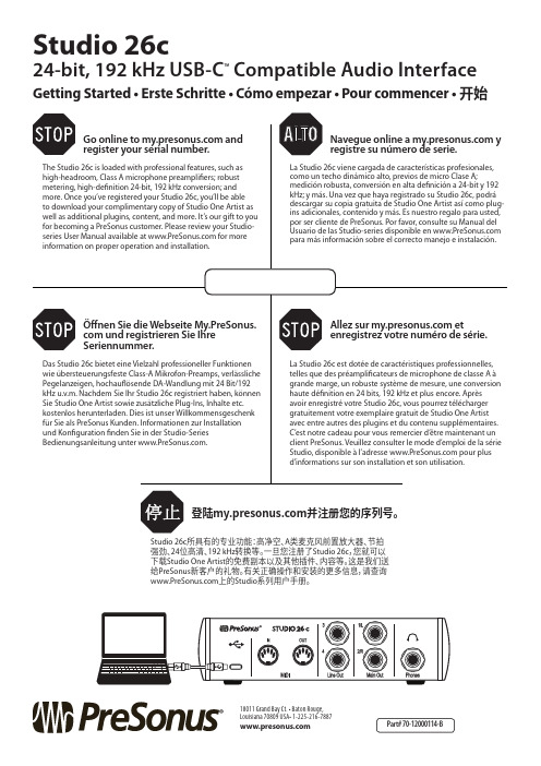
Getting Started • Erste Schritte • Cómo empezar • Pour commencer • 开始18011 Grand Bay Ct. • Baton Rouge, Louisiana 70809 USA• 1-225-216-7887®登陆并注册您的序列号。
Studio 26c 所具有的专业功能:高净空、A 类麦克风前置放大器、节拍强劲、24位高清、192 kHz 转换等。
一旦您注册了Studio 26c ,您就可以下载Studio One Artist 的免费副本以及其他插件、内容等。
这是我们送给PreSonus 新客户的礼物。
有关正确操作和安装的更多信息,请查询 上的Studio 系列用户手册。
Getting Started • Erste Schritte • Cómo empezar • Pour commencer • 开始©2019 PreSonus Audio Electronics, Inc. All Rights Reserved. The PreSonus logo is a registered trademark of PreSonus Audio Electronics, Inc. Studio One is a registered trademark of PreSonus Software, Ltd. All other trademarks are the property of their respective holders.Headphone level control Control para nivel de audífonos Regler für KopfhörerpegelCommande de niveau casque 耳机电平控制Salidas de auriculares Kopfhörerausgänge Sorties casque 耳机输出Medidores de salida principal Izquierda/DerechaAusgangspegelanzeige Main Left/RightE/S MIDI MIDI I/O Entrée/sortie MIDI 乐器数字接口(MIDI)I/O4 salidas balanceadas de línea TRS 4 symmetrische TRS-Line-Ausgänge4 sorties ligne symétriques sur jack 3 points (TRS)4个平衡TRS 线路输出。
Pro-face PS4700 Z510 15英寸工业计算机说明书

Surrounding Air Temperature Ambient/Storage Humidity Corrosive Gas Cooling Method Air Pressure (altitude range) Vibration Resistance
PS4700 Industrial PC (Z510)
Stainle AtomTM Z510 • Quick & easy storage expansion • Diskless/FANless Atom Z510
Datasheet
• TFT Color LCD Display • Power Consumption: 130W (max.) • Stainless Steel Bezel Option Available
1 Windows Embedded 2009 Only (4GB, 8GB) 2 For 16CF, Windows XP Professional is the Operating System. 3 WinGP is only preinstalled on the 16GB Compact Flash with Windows XP Professional.
Models
PS4700 Z510
Graphics Display Resolution 1024 x 768 pixels (XGA TFT active matrix)
Display Type and Size
TFT Color LCD (15-inch) (Front Bezel Material: Stainless Steel (SUS304))
AM26C31C中文资料

元器件交易网IMPORTANT NOTICETexas Instruments and its subsidiaries (TI) reserve the right to make changes to their products or to discontinueany product or service without notice, and advise customers to obtain the latest version of relevant informationto verify, before placing orders, that information being relied on is current and complete. All products are soldsubject to the terms and conditions of sale supplied at the time of order acknowledgement, including thosepertaining to warranty, patent infringement, and limitation of liability.TI warrants performance of its semiconductor products to the specifications applicable at the time of sale inaccordance with TI’s standard warranty. Testing and other quality control techniques are utilized to the extentTI deems necessary to support this warranty. Specific testing of all parameters of each device is not necessarilyperformed, except those mandated by government requirements.CERTAIN APPLICATIONS USING SEMICONDUCTOR PRODUCTS MAY INVOLVE POTENTIAL RISKS OFDEATH, PERSONAL INJURY, OR SEVERE PROPERTY OR ENVIRONMENTAL DAMAGE (“CRITICALAPPLICATIONS”). TI SEMICONDUCTOR PRODUCTS ARE NOT DESIGNED, AUTHORIZED, ORWARRANTED TO BE SUITABLE FOR USE IN LIFE-SUPPORT DEVICES OR SYSTEMS OR OTHERCRITICAL APPLICATIONS. INCLUSION OF TI PRODUCTS IN SUCH APPLICATIONS IS UNDERSTOOD TOBE FULLY AT THE CUSTOMER’S RISK.In order to minimize risks associated with the customer’s applications, adequate design and operatingsafeguards must be provided by the customer to minimize inherent or procedural hazards.TI assumes no liability for applications assistance or customer product design. TI does not warrant or representthat any license, either express or implied, is granted under any patent right, copyright, mask work right, or otherintellectual property right of TI covering or relating to any combination, machine, or process in which suchsemiconductor products or services might be or are used. TI’s publication of information regarding any thirdparty’s products or services does not constitute TI’s approval, warranty or endorsement thereof.Copyright © 1998, Texas Instruments Incorporated。
- 1、下载文档前请自行甄别文档内容的完整性,平台不提供额外的编辑、内容补充、找答案等附加服务。
- 2、"仅部分预览"的文档,不可在线预览部分如存在完整性等问题,可反馈申请退款(可完整预览的文档不适用该条件!)。
- 3、如文档侵犯您的权益,请联系客服反馈,我们会尽快为您处理(人工客服工作时间:9:00-18:30)。
.114 (2.90) .098 (2.50)
FEATURES
PAGE . 3
元器件交易网
IES
Part N umber
Marking C ode
Re v e rs e Stand -o ff Vo ltag e
Rating at 25°Cambient temperature unless otherwise specified. Resistive or inductive load, 60Hz. For Capacitive load derate current by 20%.
RATING Peak Power Dissipation at T A =25°C, T P =1ms(Note 1,2,5)Fig.1 Peak Forward Surge Current, per Figure 5(Note 3) Peak Pulse Current Current on 10/1000µs waveform(Note 1,2,5)Fig.2 Steady State Power Dissipation(Note 4) Operating and Storage Temperature Range
.062 (1.60) .055 (1.40)
.181 (4.60) .157 (4.00)
.012 (.305) .006 (.152)
.060 (1.52) .030 (0.76)
.008(.203) .002(.051) .208 (5.28) .188 (4.80)
MAXIMUM RATINGS AND CHARACTERISTICS
I PP A
M i n.
M a x. V mA
UNI
BI
UNI
BI
V
V
400W Transient Voltage Suppressor
P4SMAJ5.0 P4SMAJ5.0A P4SMAJ6.0 P4SMAJ6.0A P4SMAJ6.5 P4SMAJ6.5A P4SMAJ7.0 P4SMAJ7.0A P4SMAJ7.5 P4SMAJ7.5A P4SMAJ8.0 P4SMAJ8.0A P4SMAJ8.5 P4SMAJ8.5A P4SMAJ9.0 P4SMAJ9.0A P4SMAJ10 P4SMAJ10A P4SMAJ11 P4SMAJ11A P4SMAJ12 P4SMAJ12A P4SMAJ13 P4SMAJ13A P4SMAJ14 P4SMAJ14A P4SMAJ15 P4SMAJ15A P4SMAJ16 P4SMAJ16A P4SMAJ17 P4SMAJ17A P4SMAJ18 P4SMAJ18A P4SMAJ20 P4SMAJ20A P4SMAJ22 P4SMAJ22A P4SMAJ24 P4SMAJ24A P4SMAJ26 P4SMAJ26A P4SMAJ28 P4SMAJ28A P4SMAJ30 P4SMAJ30A P4SMAJ33 P4SMAJ33A P4SMAJ36 P4SMAJ36A P4SMAJ40 P4SMAJ40A P4SMAJ5.0C P4SMAJ5.0C A P4SMAJ6.0C P4SMAJ6.0C A P4SMAJ6.5C P4SMAJ6.5C A P4SMAJ7.0C P4SMAJ7.0C A P4SMAJ7.5C P4SMAJ7.5C A P4SMAJ8.0C P4SMAJ8.0C A P4SMAJ8.5C P4SMAJ8.5C A P4SMAJ9.0C P4SMAJ9.0C A P4SMAJ10C P4SMAJ10C A P4SMAJ11C P4SMAJ11C A P4SMAJ12C P4SMAJ12C A P4SMAJ13C P4SMAJ13C A P4SMAJ14C P4SMAJ14C A P4SMAJ15C P4SMAJ15C A P4SMAJ16C P4SMAJ16C A P4SMAJ17C P4SMAJ17C A P4SMAJ18C P4SMAJ18C A P4SMAJ20C P4SMAJ20C A P4SMAJ22C P4SMAJ22C A P4SMAJ24C P4SMAJ24C A P4SMAJ26C P4SMAJ26C A P4SMAJ28C P4SMAJ28C A P4SMAJ30C P4SMAJ30C A P4SMAJ33C P4SMAJ33C A P4SMAJ36C P4SMAJ36C A P4SMAJ40C P4SMAJ40C A HD HE HF HG HH HK HL HM HN HP HQ HR HS HT HU HV HW HX HY HZ ID IE IF IG IH IK IL IM IN IP IQ IR IS IT IU IV IW IX IY IZ JD JE JF JG JH JK JL JM JN JP JQ JR TD TE TF TG TH TK TL TM TN TP TQ TR TS TT TU TV TW TX TY TZ UD UE UF UG UH UK UL UM UN UP UQ UR US UT UU UV UW UX UY UZ VD VE VF VG VH VK VL VM VN VP VQ VR 5.0 5.0 6.0 6.0 6.5 6.5 7.0 7.0 7.5 7.5 8.0 8.0 8.5 8.5 9.0 9.0 10 10 11 11 12 12 13 13 14 14 15 15 16 16 17 17 18 18 20 20 22 22 24 24 26 26 28 28 30 30 33 33 36 36 40 40 6.40 6.40 6.67 6.67 7.22 7.22 7.78 7.78 8.33 8.33 8.89 8.89 9.44 9.44 10.0 10.0 11.1 11.1 12.2 12.2 13.3 13.3 14.4 14.4 15.6 15.6 16.7 16.7 17.8 17.8 18.9 18.9 20.0 20.0 22.2 22.2 24.4 24.4 26.7 26.7 28.9 28.9 31.1 31.1 33.3 33.3 36.7 36.7 40.0 40.0 44.4 44.4 7.55 7.25 8.45 7.67 9.14 8.30 9.86 8.95 10.67 9.58 11.30 10.23 11.92 10.82 12.6 11.5 14.1 12.8 15.4 14.0 16.9 15.3 18.2 16.5 19.8 17.9 21.1 19.2 22.6 20.5 23.9 21.7 25.3 23.3 28.1 25.5 30.9 28.0 33.8 30.7 36.6 33.2 39.4 35.8 42.2 38.3 46.5 42.2 50.7 46.0 56.3 51.1 10 10 10 10 10 10 10 10 1.0 1.0 1.0 1.0 1.0 1.0 1.0 1.0 1.0 1.0 1.0 1.0 1.0 1.0 1.0 1.0 1.0 1.0 1.0 1.0 1.0 1.0 1.0 1.0 1.0 1.0 1.0 1.0 1.0 1.0 1.0 1.0 1.0 1.0 1.0 1.0 1.0 1.0 1.0 1.0 1.0 1.0 1.0 1.0 800 800 800 800 500 500 200 200 100 100 50 50 10 10 5 5 5 5 5 5 5 5 5 5 5 5 5 5 5 5 5 5 5 5 5 5 5 5 5 5 5 5 5 5 5 5 5 5 5 5 5 5 1600 1600 1600 1600 1000 1000 400 400 200 200 100 100 20 20 10 10 5 5 5 5 5 5 5 5 5 5 5 5 5 5 5 5 5 5 5 5 5 5 5 5 5 5 5 5 5 5 5 5 5 5 5 5 9.6 9.2 11.4 S10.3 12.3 11.2 13.3 12.0 14.3 12.9 15.0 13.6 15.9 14.4 16.9 15.4 18.8 17.0 20.1 18.2 22.0 19.9 23.8 21.5 25.8 23.2 26.9 24.4 28.8 26.0 30.5 27.6 32.2 29.2 35.8 32.4 39.4 35.5 43.0 38.9 46.6 42.1 50.0 45.4 53.5 48.4 59.0 53.3 64.3 58.1 71.4 64.5 41.6 43.5 35.1 38.8 32.5 35.7 30.1 33.3 28.0 31.0 26.5 29.4 25.1 27.7 23.6 26.0 21.2 23.5 20.0 22.0 18.1 20.1 16.8 18.6 15.5 17.2 14.8 16.4 13.8 15.3 13.1 14.5 12.4 13.7 11.1 12.3 10.1 11.2 9.3 10.3 8.6 9.5 8.0 8.8 7.5 8.3 6.8 7.5 6.2 6.9 5.6 6.2 SMA/D O-214AC SMA/D O-214AC SMA/D O-214AC SMA/D O-214AC SMA/D O-214AC SMA/D O-214AC SMA/D O-214AC SMA/D O-214AC SMA/D O-214AC SMA/D O-214AC SMA/D O-214AC SMA/D O-214AC SMA/D O-214AC SMA/D O-214AC SMA/D O-214AC SMA/D O-214AC SMA/D O-214AC SMA/D O-214AC SMA/D O-214AC SMA/D O-214AC SMA/D O-214AC SMA/D O-214AC SMA/D O-214AC SMA/D O-214AC SMA/D O-214AC SMA/D O-214AC SMA/D O-214AC SMA/D O-214AC SMA/D O-214AC SMA/D O-214AC SMA/D O-214AC SMA/D O-214AC SMA/D O-214AC SMA/D O-214AC SMA/D O-214AC SMA/D O-214AC SMA/D O-214AC SMA/D O-214AC SMA/D O-214AC SMA/D O-214AC SMA/D O-214AC SMA/D O-214AC SMA/D O-214AC SMA/D O-214AC SMA/D O-214AC SMA/D O-214AC SMA/D O-214AC SMA/D O-214AC SMA/D O-214AC SMA/D O-214AC SMA/D O-214AC SMA/D O-214AC