SN74LS243中文资料
74LS243中文资料
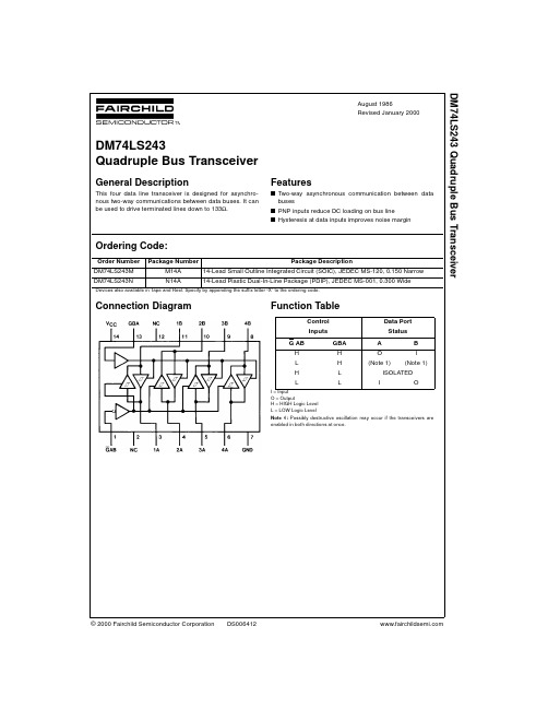
© 2000 Fairchild Semiconductor Corporation DS006412August 1986Revised January 2000DM74LS243 Quadruple Bus TransceiverDM74LS243Quadruple Bus TransceiverGeneral DescriptionThis four data line transceiver is designed for asynchro-nous two-way communications between data buses. It can be used to drive terminated lines down to 133Ω.Featuress Two-way asynchronous communication between data buses s PNP inputs reduce DC loading on bus line s Hysteresis at data inputs improves noise marginOrdering Code:Devices also available in T ape and Reel. Specify by appending the suffix letter “X” to the ordering code.Connection Diagram Function TableI = Input O = OutputH = HIGH Logic Level L = LOW Logic LevelNote 1: Possibly destructive oscillation may occur if the transceivers are enabled in both directions at once.Order Number Package NumberPackage DescriptionDM74LS243M M14A 14-Lead Small Outline Integrated Circuit (SOIC), JEDEC MS-120, 0.150 Narrow DM74LS243NN14A14-Lead Plastic Dual-In-Line Package (PDIP), JEDEC MS-001, 0.300 WideControl Data Port InputsStatusG AB GBA A B H H O I L H (Note 1)(Note 1)H L ISOLATEDLLI O 2D M 74L S 243Absolute Maximum Ratings (Note 2)Note 2: The “Absolute Maximum Ratings” are those values beyond which the safety of the device cannot be guaranteed. The device should not be operated at these limits. The parametric values defined in the Electrical Characteristics tables are not guaranteed at the absolute maximum ratings.The “Recommended Operating Conditions” table will define the conditions for actual device operation.Recommended Operating ConditionsElectrical Characteristicsover recommended operating free air temperature range (unless otherwise noted)Note 3: All typicals are at V CC = 5V, T A = 25°C.Note 4: Not more than one output should be shorted at a time, and the duration should not exceed one second.Supply Voltage 7VInput Voltage Any G 7V A or B5.5VOperating Free Air Temperature Range 0°C to +70°C Storage Temperature Range−65°C to +150°CSymbol ParameterMin Nom Max Units V CC Supply Voltage4.7555.25V V IH HIGH Level Input Voltage 2V V IL LOW Level Input Voltage 0.8V I OH HIGH Level Output Current −15mA I OL LOW Level Output Current 24mA T AFree Air Operating Temperature70°CSymbol ParameterConditions MinTyp Max Units (Note 3)V I Input Clamp Voltage V CC = Min, I I = −18 mA −1.5V HYS Hysteresis (V T + − V T −)V CC = Min0.20.4V(Data Inputs Only)V OHHIGH Level Output VoltageV CC = Min, V IH = Min 2.7V IL = Max, I OH = −1 mA V CC = Min, V IH = Min 2.4 3.4VV IL = Max, I OH = −3 mA V CC = Min, V IH = Min 2V IL = 0.5V, I OH = MaxV OLLOW Level Output VoltageV CC = Min I OL = 12 mA 0.4V IL = Max I OL = MaxVV IH = Min0.5I OZH Off-State Output Current,V CC = Max V O = 2.7V 40µA HIGH Level Voltage Applied V IL = Max I OZL Off-State Output Current,V IH = MinV O = 0.4V−200µA LOW Level Voltage Applied I I Input Current at Maximum V CC = MaxV I = 5.5V A or B 0.1mA Input VoltageV I = 7VAny G0.1mA I IH HIGH Level Input Current V CC = Max, V I = 2.7V 20µA I IL LOW Level Input Current V CC = Max, V I = 0.4V −0.2mA I OS Short Circuit Output Current V CC = Max (Note 4)−40−225mAI CCSupply CurrentV CC = Max Outputs HIGH 2238Outputs Outputs LOW 2950mA OPENOutputs Disabled3254DM74LS243 Switching Characteristicsat V CC= 5V, T A= 25°CSymbol Parameter Conditions Min Max Unitst PLH Propagation Delay Time C L= 45 pF18ns LOW-to-HIGH Level Output R L= 667Ωt PHL Propagation Delay Time C L= 45 pF18ns HIGH-to-LOW Level Output R L= 667Ωt PZL Output Enable Time C L= 45 pF30ns to LOW Level R L= 667Ωt PZH Output Enable Time C L= 45 pF23ns to HIGH Level R L= 667Ωt PLZ Output Disable Time C L= 5 pF25ns from LOW Level R L= 667Ωt PHZ Output Disable Time C L= 5 pF18ns from HIGH Level R L= 667Ωt PLH Propagation Delay Time C L= 150 pF21ns LOW-to-HIGH Level Output R L= 667Ωt PHL Propagation Delay Time C L= 150 pF22ns HIGH-to-LOW Level Output R L= 667Ωt PZL Output Enable Time C L= 150 pF33ns to LOW Level R L= 667Ωt PZH Output Enable Time C L= 150 pF26ns to HIGH Level R L= 667Ω 4D M 74L S 243Physical Dimensionsinches (millimeters) unless otherwise noted14-Lead Small Outline Integrated Circuit (SOIC), JEDEC MS-120, 0.150 NarrowPackage Number M14A5DM74LS243 Quadruple Bus TransceiverPhysical Dimensions inches (millimeters) unless otherwise noted (Continued)14-Lead Plastic Dual-In-Line Package (PDIP), JEDEC MS-001, 0.300 WidePackage Number N14AFairchild does not assume any responsibility for use of any circuitry described, no circuit patent licenses are implied and Fairchild reserves the right at any time without notice to change said circuitry and specifications.LIFE SUPPORT POLICYFAIRCHILD’S PRODUCTS ARE NOT AUTHORIZED FOR USE AS CRITICAL COMPONENTS IN LIFE SUPPORT DEVICES OR SYSTEMS WITHOUT THE EXPRESS WRITTEN APPROVAL OF THE PRESIDENT OF FAIRCHILD SEMICONDUCTOR CORPORATION. As used herein:1.Life support devices or systems are devices or systems which, (a) are intended for surgical implant into the body, or (b) support or sustain life, and (c) whose failure to perform when properly used in accordance with instructions for use provided in the labeling, can be rea-sonably expected to result in a significant injury to the user.2. A critical component in any component of a life support device or system whose failure to perform can be rea-sonably expected to cause the failure of the life support device or system, or to affect its safety or effectiveness.。
SN74LS123D中文资料
PRODUCTION DATA information is current as of publication date.Products conform to specifications per the terms of Texas Instrumentsstandard warranty. Production processing does not necessarily includetesting of all parameters.1POST OFFICE BOX 655303 • DALLAS, TEXAS 752652POST OFFICE BOX 655303 • DALLAS, TEXAS 752653 POST OFFICE BOX 655303 • DALLAS, TEXAS 752654POST OFFICE BOX 655303 • DALLAS, TEXAS 752655 POST OFFICE BOX 655303 • DALLAS, TEXAS 752656POST OFFICE BOX 655303 • DALLAS, TEXAS 752657 POST OFFICE BOX 655303 • DALLAS, TEXAS 752658POST OFFICE BOX 655303 • DALLAS, TEXAS 752659 POST OFFICE BOX 655303 • DALLAS, TEXAS 75265PACKAGING INFORMATIONOrderable Device Status (1)Package Type Package DrawingPins Package Qty Eco Plan (2)Lead/Ball FinishMSL Peak Temp (3)5962-7603901VEA ACTIVE CDIP J 161None Call TI Level-NC-NC-NC 5962-7603901VFAACTIVE CFP W 161None Call TI Level-NC-NC-NC 7603901EA ACTIVE CDIP J 161None Call TI Level-NC-NC-NC 7603901FA ACTIVE CFP W 161None Call TI Level-NC-NC-NC JM38510/01203BEA ACTIVE CDIP J 161None Call TI Level-NC-NC-NC JM38510/31401B2A ACTIVE LCCC FK 201None Call TI Level-NC-NC-NC JM38510/31401BEA ACTIVE CDIP J 161None Call TI Level-NC-NC-NC JM38510/31401BFAACTIVE CFP W 161None Call TI Level-NC-NC-NC SN54122J OBSOLETE CDIP J 14None Call TI Call TISN54123J ACTIVE CDIP J 161None Call TI Level-NC-NC-NC SN54LS123J ACTIVE CDIP J 161None Call TI Level-NC-NC-NC SN74122N OBSOLETE PDIP N 14None Call TI Call TISN74123N ACTIVE PDIP N 1625Pb-Free (RoHS)CU NIPDAU Level-NC-NC-NC SN74123N3OBSOLETE PDIP N 16None Call TI Call TISN74LS122D ACTIVE SOIC D 1450Pb-Free (RoHS)CU NIPDAU Level-2-260C-1YEAR/Level-1-235C-UNLIM SN74LS122DR ACTIVE SOIC D 142500Pb-Free (RoHS)CU NIPDAU Level-2-260C-1YEAR/Level-1-235C-UNLIM SN74LS122N ACTIVE PDIP N 1425Pb-Free (RoHS)CU NIPDAU Level-NC-NC-NC SN74LS122N3OBSOLETE PDIP N 14None Call TI Call TISN74LS122NSR ACTIVE SO NS 142000Pb-Free (RoHS)CU NIPDAU Level-2-260C-1YEAR/Level-1-235C-UNLIM SN74LS123D ACTIVE SOIC D 1640Pb-Free (RoHS)CU NIPDAU Level-2-260C-1YEAR/Level-1-235C-UNLIM SN74LS123DR ACTIVE SOIC D 162500Pb-Free (RoHS)CU NIPDAU Level-2-260C-1YEAR/Level-1-235C-UNLIM SN74LS123J OBSOLETE CDIP J 16None Call TI Call TISN74LS123N ACTIVE PDIP N 1625Pb-Free (RoHS)CU NIPDAU Level-NC-NC-NC SN74LS123N3OBSOLETE PDIP N 16None Call TI Call TISN74LS123NSR ACTIVE SO NS 162000Pb-Free (RoHS)CU NIPDAU Level-2-260C-1YEAR/Level-1-235C-UNLIM SNJ54122J OBSOLETE CDIP J 14None Call TI Call TISNJ54123J ACTIVE CDIP J 161None Call TI Level-NC-NC-NC SNJ54123W ACTIVE CFP W 161None Call TI Level-NC-NC-NC SNJ54LS123FK ACTIVE LCCC FK 201None Call TI Level-NC-NC-NC SNJ54LS123J ACTIVE CDIP J 161None Call TI Level-NC-NC-NC SNJ54LS123WACTIVECFPW161NoneCall TILevel-NC-NC-NC(1)The marketing status values are defined as follows:ACTIVE:Product device recommended for new designs.LIFEBUY:TI has announced that the device will be discontinued,and a lifetime-buy period is in effect.NRND:Not recommended for new designs.Device is in production to support existing customers,but TI does not recommend using this part in a new design.PREVIEW:Device has been announced but is not in production.Samples may or may not be available.PACKAGE OPTION ADDENDUM28-Feb-2005Addendum-Page 1元器件交易网OBSOLETE:TI has discontinued the production of the device.(2)Eco Plan -May not be currently available -please check /productcontent for the latest availability information and additional product content details.None:Not yet available Lead (Pb-Free).Pb-Free (RoHS):TI's terms "Lead-Free"or "Pb-Free"mean semiconductor products that are compatible with the current RoHS requirements for all 6substances,including the requirement that lead not exceed 0.1%by weight in homogeneous materials.Where designed to be soldered at high temperatures,TI Pb-Free products are suitable for use in specified lead-free processes.Green (RoHS &no Sb/Br):TI defines "Green"to mean "Pb-Free"and in addition,uses package materials that do not contain halogens,including bromine (Br)or antimony (Sb)above 0.1%of total product weight.(3)MSL,Peak Temp.--The Moisture Sensitivity Level rating according to the JEDECindustry standard classifications,and peak solder temperature.Important Information and Disclaimer:The information provided on this page represents TI's knowledge and belief as of the date that it is provided.TI bases its knowledge and belief on information provided by third parties,and makes no representation or warranty as to the accuracy of such information.Efforts are underway to better integrate information from third parties.TI has taken and continues to take reasonable steps to provide representative and accurate information but may not have conducted destructive testing or chemical analysis on incoming materials and chemicals.TI and TI suppliers consider certain information to be proprietary,and thus CAS numbers and other limited information may not be available for release.In no event shall TI's liability arising out of such information exceed the total purchase price of the TI part(s)at issue in this document sold by TI to Customer on an annualbasis.PACKAGE OPTION ADDENDUM 28-Feb-2005Addendum-Page 2IMPORTANT NOTICETexas Instruments Incorporated and its subsidiaries (TI) reserve the right to make corrections, modifications, enhancements, improvements, and other changes to its products and services at any time and to discontinue any product or service without notice. Customers should obtain the latest relevant information before placing orders and should verify that such information is current and complete. All products are sold subject to TI’s terms and conditions of sale supplied at the time of order acknowledgment.TI warrants performance of its hardware products to the specifications applicable at the time of sale in accordance with TI’s standard warranty. T esting and other quality control techniques are used to the extent TI deems necessary to support this warranty. Except where mandated by government requirements, testing of all parameters of each product is not necessarily performed.TI assumes no liability for applications assistance or customer product design. Customers are responsible for their products and applications using TI components. T o minimize the risks associated with customer products and applications, customers should provide adequate design and operating safeguards.TI does not warrant or represent that any license, either express or implied, is granted under any TI patent right, copyright, mask work right, or other TI intellectual property right relating to any combination, machine, or process in which TI products or services are used. Information published by TI regarding third-party products or services does not constitute a license from TI to use such products or services or a warranty or endorsement thereof. Use of such information may require a license from a third party under the patents or other intellectual property of the third party, or a license from TI under the patents or other intellectual property of TI.Reproduction of information in TI data books or data sheets is permissible only if reproduction is without alteration and is accompanied by all associated warranties, conditions, limitations, and notices. Reproduction of this information with alteration is an unfair and deceptive business practice. TI is not responsible or liable for such altered documentation.Resale of TI products or services with statements different from or beyond the parameters stated by TI for that product or service voids all express and any implied warranties for the associated TI product or service and is an unfair and deceptive business practice. TI is not responsible or liable for any such statements. Following are URLs where you can obtain information on other Texas Instruments products and application solutions:Products ApplicationsAmplifiers Audio /audioData Converters Automotive /automotiveDSP Broadband /broadbandInterface Digital Control /digitalcontrolLogic Military /militaryPower Mgmt Optical Networking /opticalnetwork Microcontrollers Security /securityTelephony /telephonyVideo & Imaging /videoWireless /wirelessMailing Address:Texas InstrumentsPost Office Box 655303 Dallas, Texas 75265Copyright 2005, Texas Instruments Incorporated。
74ls123中文资料汇总(74ls123引脚图及功能

74ls123中文资料汇总(74ls123引脚图及功能74ls123推荐工作条件74ls123静态特性【1】:测试条件中的“最大”和“最小”用推荐工作条件中的相应值。
【2】:若在Q测VOH,/Q测VOL,Q测IOS时:'123 的Cext 接地;LS123 的Rext/Cext接地,B和CLR接VIH,A接 2V到 0V的脉冲电压。
若在/Q 测 VOH、Q 测 VOL、/Q 测 IOS 时:'123 的 Cext 开路【3】:测'123 时:Cext=0.02μF,Rext=25kΩ。
静态:所有A 和 CLR 接 2.4V,所有 B 接地。
触发态:所有 B 和 CLR 接 2.4V,所有 B 接地。
测'LS123 时:所有 A、B、CLR 接 4.5V,时钟瞬时接地后接 4.5V。
74ls123动态特性【4】:tPLH-输出由低到高电平传输延迟时间tPHL-输出由高到低电平传输延迟时间tWQ-Q端输出脉冲宽度三款74ls123应用电路及原理应用电路一:振铃检测、模拟摘机电路如图2,振铃检测电路是由光耦TLP521-1和74LS123构成。
当有电话呼入时,电话线上传输的25HZ、90V 的交流振铃信号由C1、C2隔离直流后由整流桥整流,整流后的直流电压值较高,经光电隔离器U1后输出TTL脉冲信号,该脉冲经74LS123整形成大方波信号,该方波信号送至单片机的P3.5引脚进行计数,当计数值达到预设值时,单片机P1.0引脚输出高电平,三极管Q1导通则继电器K1动作,将负载电阻R5(330Ω)接入电路实现模拟摘机。
这里所说的模拟摘机是指将R5接入电路后,电话线上就会出现大于10mA的电流,交换中心检测到这一电流后就不再输出振铃信号而是转为接通电话。
人们手动摘机接通电话时的工作过程与此一致,因此称为模拟摘机。
如果振铃信号没有达到预设值就消失,则单片机的计数值清零,控制器不动作。
TTL74系列芯片大全(中英文对照)

7400 TTL 2输入端四与非门7401 TTL 集电极开路2输入端四与非门7402 TTL 2输入端四或非门7403 TTL 集电极开路2输入端四与非门7404 TTL 六反相器7405 TTL 集电极开路六反相器7406 TTL 集电极开路六反相高压驱动器7407 TTL 集电极开路六正相高压驱动器7408 TTL 2输入端四与门7409 TTL 集电极开路2输入端四与门7410 TTL 3输入端3与非门74107 TTL 带清除主从双J-K触发器74109 TTL 带预置清除正触发双J-K触发器7411 TTL 3输入端3与门74112 TTL 带预置清除负触发双J-K触发器7412 TTL 开路输出3输入端三与非门74121 TTL 单稳态多谐振荡器74122 TTL 可再触发单稳态多谐振荡器74123 TTL 双可再触发单稳态多谐振荡器74125 TTL 三态输出高有效四总线缓冲门74126 TTL 三态输出低有效四总线缓冲门7413 TTL 4输入端双与非施密特触发器74132 TTL 2输入端四与非施密特触发器74133 TTL 13输入端与非门74136 TTL 四异或门74138 TTL 3-8线译码器/复工器74139 TTL 双2-4线译码器/复工器7414 TTL 六反相施密特触发器74145 TTL BCD—十进制译码/驱动器7415 TTL 开路输出3输入端三与门74150 TTL 16选1数据选择/多路开关74151 TTL 8选1数据选择器74153 TTL 双4选1数据选择器74154 TTL 4线—16线译码器74155 TTL 图腾柱输出译码器/分配器74156 TTL 开路输出译码器/分配器74157 TTL 同相输出四2选1数据选择器74158 TTL 反相输出四2选1数据选择器7416 TTL 开路输出六反相缓冲/驱动器74160 TTL 可预置BCD异步清除计数器74161 TTL 可予制四位二进制异步清除计数器74162 TTL 可预置BCD同步清除计数器74163 TTL 可予制四位二进制同步清除计数器74164 TTL 八位串行入/并行输出移位寄存器74165 TTL 八位并行入/串行输出移位寄存器74166 TTL 八位并入/串出移位寄存器74169 TTL 二进制四位加/减同步计数器7417 TTL 开路输出六同相缓冲/驱动器74170 TTL 开路输出4×4寄存器堆74173 TTL 三态输出四位D型寄存器74174 TTL 带公共时钟和复位六D触发器74175 TTL 带公共时钟和复位四D触发器74180 TTL 9位奇数/偶数发生器/校验器74181 TTL 算术逻辑单元/函数发生器74185 TTL 二进制—BCD代码转换器74190 TTL BCD同步加/减计数器74191 TTL 二进制同步可逆计数器74192 TTL 可预置BCD双时钟可逆计数器74193 TTL 可预置四位二进制双时钟可逆计数器74194 TTL 四位双向通用移位寄存器74195 TTL 四位并行通道移位寄存器74196 TTL 十进制/二-十进制可预置计数锁存器74197 TTL 二进制可预置锁存器/计数器7420 TTL 4输入端双与非门7421 TTL 4输入端双与门7422 TTL 开路输出4输入端双与非门74221 TTL 双/单稳态多谐振荡器74240 TTL 八反相三态缓冲器/线驱动器74241 TTL 八同相三态缓冲器/线驱动器74243 TTL 四同相三态总线收发器74244 TTL 八同相三态缓冲器/线驱动器74245 TTL 八同相三态总线收发器74247 TTL BCD—7段15V输出译码/驱动器74248 TTL BCD—7段译码/升压输出驱动器74249 TTL BCD—7段译码/开路输出驱动器74251 TTL 三态输出8选1数据选择器/复工器74253 TTL 三态输出双4选1数据选择器/复工器74256 TTL 双四位可寻址锁存器74257 TTL 三态原码四2选1数据选择器/复工器74258 TTL 三态反码四2选1数据选择器/复工器74259 TTL 八位可寻址锁存器/3-8线译码器7426 TTL 2输入端高压接口四与非门74260 TTL 5输入端双或非门74266 TTL 2输入端四异或非门7427 TTL 3输入端三或非门74273 TTL 带公共时钟复位八D触发器74279 TTL 四图腾柱输出S-R锁存器7428 TTL 2输入端四或非门缓冲器74283 TTL 4位二进制全加器74290 TTL 二/五分频十进制计数器74293 TTL 二/八分频四位二进制计数器74295 TTL 四位双向通用移位寄存器74298 TTL 四2输入多路带存贮开关74299 TTL 三态输出八位通用移位寄存器7430 TTL 8输入端与非门7432 TTL 2输入端四或门74322 TTL 带符号扩展端八位移位寄存器74323 TTL 三态输出八位双向移位/存贮寄存器7433 TTL 开路输出2输入端四或非缓冲器74347 TTL BCD—7段译码器/驱动器74352 TTL 双4选1数据选择器/复工器74353 TTL 三态输出双4选1数据选择器/复工器74365 TTL 门使能输入三态输出六同相线驱动器74365 TTL 门使能输入三态输出六同相线驱动器74366 TTL 门使能输入三态输出六反相线驱动器74367 TTL 4/2线使能输入三态六同相线驱动器74368 TTL 4/2线使能输入三态六反相线驱动器7437 TTL 开路输出2输入端四与非缓冲器74373 TTL 三态同相八D锁存器74374 TTL 三态反相八D锁存器74375 TTL 4位双稳态锁存器74377 TTL 单边输出公共使能八D锁存器74378 TTL 单边输出公共使能六D锁存器74379 TTL 双边输出公共使能四D锁存器7438 TTL 开路输出2输入端四与非缓冲器74380 TTL 多功能八进制寄存器7439 TTL 开路输出2输入端四与非缓冲器74390 TTL 双十进制计数器74393 TTL 双四位二进制计数器7440 TTL 4输入端双与非缓冲器7442 TTL BCD—十进制代码转换器74352 TTL 双4选1数据选择器/复工器74353 TTL 三态输出双4选1数据选择器/复工器74365 TTL 门使能输入三态输出六同相线驱动器74366 TTL 门使能输入三态输出六反相线驱动器74367 TTL 4/2线使能输入三态六同相线驱动器74368 TTL 4/2线使能输入三态六反相线驱动器7437 TTL 开路输出2输入端四与非缓冲器74373 TTL 三态同相八D锁存器74374 TTL 三态反相八D锁存器74375 TTL 4位双稳态锁存器74377 TTL 单边输出公共使能八D锁存器74378 TTL 单边输出公共使能六D锁存器74379 TTL 双边输出公共使能四D锁存器7438 TTL 开路输出2输入端四与非缓冲器74380 TTL 多功能八进制寄存器7439 TTL 开路输出2输入端四与非缓冲器74390 TTL 双十进制计数器74393 TTL 双四位二进制计数器7440 TTL 4输入端双与非缓冲器7442 TTL BCD—十进制代码转换器74447 TTL BCD—7段译码器/驱动器7445 TTL BCD—十进制代码转换/驱动器74450 TTL 16:1多路转接复用器多工器74451 TTL 双8:1多路转接复用器多工器74453 TTL 四4:1多路转接复用器多工器7446 TTL BCD—7段低有效译码/驱动器74460 TTL 十位比较器74461 TTL 八进制计数器74465 TTL 三态同相2与使能端八总线缓冲器74466 TTL 三态反相2与使能八总线缓冲器74467 TTL 三态同相2使能端八总线缓冲器74468 TTL 三态反相2使能端八总线缓冲器74469 TTL 八位双向计数器7447 TTL BCD—7段高有效译码/驱动器7448 TTL BCD—7段译码器/内部上拉输出驱动74490 TTL 双十进制计数器74491 TTL 十位计数器74498 TTL 八进制移位寄存器7450 TTL 2-3/2-2输入端双与或非门74502 TTL 八位逐次逼近寄存器74503 TTL 八位逐次逼近寄存器7451 TTL 2-3/2-2输入端双与或非门74533 TTL 三态反相八D锁存器74534 TTL 三态反相八D锁存器7454 TTL 四路输入与或非门74540 TTL 八位三态反相输出总线缓冲器7455 TTL 4输入端二路输入与或非门74563 TTL 八位三态反相输出触发器74564 TTL 八位三态反相输出D触发器74573 TTL 八位三态输出触发器74574 TTL 八位三态输出D触发器74645 TTL 三态输出八同相总线传送接收器74670 TTL 三态输出4×4寄存器堆7473 TTL 带清除负触发双J-K触发器7474 TTL 带置位复位正触发双D触发器7476 TTL 带预置清除双J-K触发器7483 TTL 四位二进制快速进位全加器7485 TTL 四位数字比较器7486 TTL 2输入端四异或门7490 TTL 可二/五分频十进制计数器7493 TTL 可二/八分频二进制计数器7495 TTL 四位并行输入\输出移位寄存器7497 TTL 6位同步二进制乘法器SN74LSOO四2输入与非门SN74LSO2四2输入或非门SN74LS04六反相器SN74LS06六反相缓冲器/驱动器SN74LS08四2输入与非门SN74LS10三3输入与非门SN74LS12三3输入与非门SN74LS14六反相器.斯密特触发SN74LS16六反相缓冲器/驱动器SN74LS20双4输入与门SN74LS22双4输入与门SN74LS26四2输入与非门SN74LS28四输入端或非缓冲器SN74LS32四2输入或门SN74LS37四输入端与非缓冲器SN74LS40四输入端与非缓冲器SN74LS47BCD-七段译码驱动器SN74LS49BCD-七段译码驱动器SN74LS54四输入与或非门SN74LS63六电流读出接口门SN74LS74双D触发器SN74LS76双J-K触发器SN74LS83双J-K触发器SN74LS86四2输入异或门SN74LS904位十进制波动计数器SN74LS9212分频计数器SN74LS965位移位寄存器SN74LS109正沿触发双J-K触发器SN74LS113双J-K负沿触发器SN74LS121单稳态多谐振荡器SN74LS123双稳态多谐振荡器SN74LS125三态缓冲器SN74LS1313-8线译码器SN74LS13313输入与非门SN74LS137地址锁存3-8线译码器SN74LS139双2-4线译码-转换器SN74LS14710-4线优先编码器SN74LS153双4选1数据选择器SN74LS155双2-4线多路分配器SN74LS157四2选1数据选择器SN74LS160同步BDC十进制计数器SN74LS162同步BDC十进制计数器SN74LS1648位串入并出移位寄存SN74LS1668位移位寄存器SN74LS1694位可逆同步计数器SN74LS17216位多通道寄存器堆SN74LS1746D型触发器SN74LS176可预置十进制计数器SN74LS182超前进位发生器SN74LS18964位随机存储器SN74LS191二进制同步可逆计数器SN74LS193二进制可逆计数器SN74LS195并行存取移位寄存器SN74LS197可预置二进制计数器SN74LS2383-8线译码/多路转换器SN74LS241八缓冲/驱动/接收器SN74LS243四总线收发器SN74LS245八总线收发器SN74LS248BCD-七段译码驱动器SN74LS251三态8-1数据选择器SN74LS256双四位选址锁存器SN74LS258四2选1数据选择器SN74LS260双5输入或非门SN74LS266四2输入异或非门SN74LS275七位树型乘法器SN74LS279四R-S触发器SN74LS2834位二进制全加器SN74LS2934位二进制计数器SN74LS365六缓冲器带公用启动器SN74LS367六总线三态输出缓冲器SN74LS3738D锁存器SN74LS3754位双稳锁存器SN74LS386四2输入异或门SN74LS393双4位二进制计数器SN74LS5748位D型触发器SN74LS6848位数字比较器SN74LSO1四2输入与非门SN74LS03四2输入与非门SN74LS05六反相器SN74LS07六缓冲器/驱动器SN74LS09四2输入与非门SN74LS11三3输入与非门SN74LS13三3输入与非门SN74LS15三3输入与非门SN74LS17六反相缓冲器/驱动器SN74LS21双4输入与门SN74LS25双4输入与门SN74LS27三3输入与非门SN74LS30八输入端与非门SN74LS33四2输入或门SN74LS38双2输入与非缓冲器SN74LS42BCD-十进制译码器SN74LS48BCD-七段译码驱动器SN74LS51三3输入双与或非门SN74LS55四4输入与或非门SN74LS73双J-K触发器SN74LS754位双稳锁存器SN74LS78双J-K触发器SN74LS854位幅度比较器SN74LS884位全加器SN74LS918位移位寄存器SN74LS93二进制计数器SN74LS954位并入并出寄存器SN74LS107双J-K触发器SN74LS112双J-K负沿触发器SN74LS114双J-K负沿触发器SN74LS122单稳态多谐振荡器SN74LS124双压控振荡器SN74LS126四3态总线缓冲器SN74LS132二输入与非触发器SN74LS136四异或门SN74LS1383-8线译码/转换器SN74LS145BCD十进制译码/驱动器SN74LS1488-3线优先编码器SN74LS1518选1数据选择器SN74LS1544-16线多路分配器SN74LS156双2-4线多路分配器SN74LS158四2选1数据选择器SN74LS1614位二进制计数器SN74LS1634位二进制计数器SN74LS1658位移位寄存器SN74LS1684位可逆同步计数器SN74LS1704x4位寄存器堆SN74LS1734D型寄存器SN74LS1754D烯触发器SN74LS181运算器/函数发生器SN74LS183双进位保存全价器SN74LS190同步BCD十进制计数器SN74LS192BCD-同步可逆计数器SN74LS194双向通用移位寄存器SN74LS196可预置十进制计数器SN74LS221双单稳态多谐振荡器SN74LS240八缓冲/驱动/接收器SN74LS242四总线收发器SN74LS244八缓冲/驱动/接收器SN74LS247BCD-七段译码驱动器SN74LS249BCD-七段译码驱动SN74LS253双三态4-1数据选择器SN74LS257四3态2-1数据选择器SN74LS2598位可寻址锁存器SN74LS2612x4位二进制乘发器SN74LS273八进制D型触发器SN74LS276四J-K触发器SN74LS2809位奇偶数发生校检器SN74LS290十进制计数器SN74LS2954位双向通用移位寄存器SN74LS366六缓冲器带公用启动器SN74LS368六总线三态输出反相器SN74LS3748D触发器SN74LS3778位单输出D型触发器SN74LS390双十进制计数器SN74LS5738位三态输出D型锁存器SN74LS6708位数字比较器SN74HC00 四2输入与非门SN74HC02 四2输入或非门SN74HC03 四2输入或非门SN74HC04 六反相器SN74HC05 六反相器SN74HC08 四2输入与门SN74HC10 三3输入与非门SN74HC11 三3输入与门SN74HC14 六反相器/斯密特触发SN74HC20 双四输入与门SN74HC21 双四输入与非门SN74HC27 三3输入与非门SN74HC30 八输入端与非门SN74HC32 四2输入或门SN74HC42 BCD十进制译码器SN74HC73 双J-K触的器SN74HC76 双J-K触的器SN74HC86 四2输入异或门SN74HC107 双J-K触发器SN74HC113 双J-K负沿触发器SN74HC123 双稳态多谐振荡器SN74HC125 三态缓冲器SN74HC126 四三态总线缓冲器SN74HC132 二输入与非缓冲器SN74HC137 二输入与非缓冲器SN74HC138 3-8线译码/解调器SN74HC139 双2-4线译码/解调器SN74HC148 8选1数据选择器SN74HC151 双4选1数据选择器SN74HC154 4-16线多路分配器SN74HC157 四2选1数据选择器SN74HC161 4位二进制计数器SN74HC163 4位二进制计数器SN74HC164 8位串入并出移位寄存器SN74HC165 8位移位寄存器SN74HC173 4D型触发器SN74HC174 6D触发器SN74HC175 4D型触发器SN74HC191 二进制同步可逆计数器SN74HC221 双单稳态多谐振荡器SN74HC238 3-8线译码器SN74HC240 八缓冲器SN74HC244 八总线3态输出缓冲器SN74HC245 八总线收发器SN74HC251 三态8-1数据选择器SN74HC259 8位可寻址锁存器SN74HC266 四2输入异或非门SN74HC273 8D型触发器SN74HC367 六缓冲器/总线驱动器SN74HC368 六缓冲器/总线驱动器SN74HC373 8D锁存器SN74HC374 8D触发器SN74HC393 双4位二进制计数器SN74HC541 8位三态输出缓冲器SN74HC573 8位三态输出D型锁存器SN74HC574 8D型触发器SN74HC595 8位移位寄存器/锁存器SN74HC4028 7级二进制串行加数器SN74HC4046 锁相环SN74HC4051 8选1模拟开关SN74HC4053 三2选1模拟开关SN74HC4060 14位计数/分频/振荡器SN74HC4066 四双相模拟开关SN74HC4078 3输入端三或门SN74HC4511 7段锁存/译码驱动器SN74HC4520 双二进制加法计数器74F00 高速四2输入与非门74F02 高速四2输入或非门74F04 高速六反相器74F08 高速四2输入与门74F10 高速三3输入与门74F14 高速六反相斯密特触发74F32 高速四2输入或门74F38 高速四2输入或门74F74 高速双D型触发器74F86 高速四2输入异或门74F139 高速双2-4线译码/驱动器74F151 高速双2-4线译码/驱动器74F153 高速双4选1数据选择器74F157 高速双4选1数据选择器74F161 高速6D型触发器74F174 高速6D型触发器74F175 高速4D型触发器74F244 高速八总线3态缓冲器74F245 高速八总线收发器74F373 高速8D锁存器SN74HCT04 六反相器。
关于74ls244和74ls273两个芯片的介绍

关于74ls244和74ls273两个芯片的介绍74LS244为3态8位地址锁存器。
地址锁存器就是一个暂存器,它根据控制信号的状态,将总线上地址代码暂存起来。
8086/8088数据和地址总线采用分时复用操作方法,即用同一总线既传输数据又传输地址。
当微处理器与存储器交换信号时,首先由CPU发出存储器地址,同时发出允许锁存信号ALE给锁存器,当锁存器接到该信号后将地址/数据总线上的地址锁存在总线上,随后才能传输数据。
锁存器是一个很普通的时序电路。
一般的,它在时钟上升沿或者下降沿来的时候锁存输入,然后产生输出,在其他的时候输出都不跟随输入变化,这就是所谓边缘触发的D触发器。
当然也有电平触发的D触发器,具体使用哪种,得看你使用得总线配置。
通常用作单片机的地址锁存器的芯片有74LS373、8282、74LS273等。
74LS373和8282是带三态输出的8位锁存器,它们的结构和用法类似。
以74LS373为例,共有8个输入端D1—D8及8个输出端Q1—Q8。
当三态端OE为有效低电平,74LS373的G端为输人选通端,使能端G为有效高电平时,输出跟随输入变化;当G=1时,锁存器处于透明工作状态,即锁存器的输出状态随数据端的变化而变化,即脚1=Di(I=1,2,…,8)。
当G端由1变0时,数据被锁存起来,此时输出端Qi不再随输入端的变化而变化,而一直保持锁存前的值不变。
G端(或STB端)可直接与单片机的锁存控制信号端ALE相连,在ALE的下降沿进行地址锁存。
只要根据“输入三态,输出锁存”的原则,选择74系列的TTL电路或MOS电路就能组成简单的扩展电路,如74LS244、74LS273、74LS373、74LS377等芯片都能组成输入、输出接口。
SN74LS240中文资料
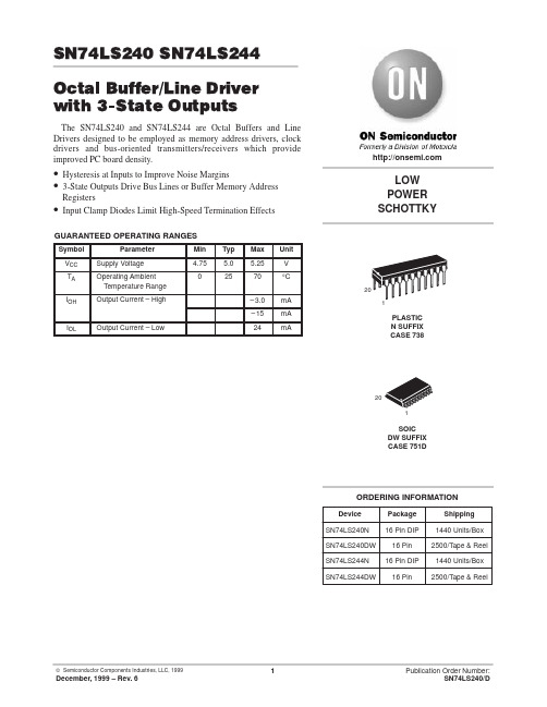
LOW POWER SCHOTTKYDevice Package Shipping SN74LS240N 16 Pin DIP 1440 Units/Box SN74LS240DW 16 Pin SOIC DW SUFFIX CASE 751D2500/T ape & Reel PLASTIC N SUFFIX CASE 738201201SN74LS244N 16 Pin DIP 1440 Units/Box SN74LS244DW16 Pin2500/T ape & ReelON Semiconductor and are trademarks of Semiconductor Components Industries, LLC (SCILLC). SCILLC reserves the right to make changes without further notice to any products herein. SCILLC makes no warranty, representation or guarantee regarding the suitability of its products for any particular purpose, nor does SCILLC assume any liability arising out of the application or use of any product or circuit, and specifically disclaims any and all liability, including without limitation special, consequential or incidental damages. “Typical” parameters which may be provided in SCILLC data sheets and/or specifications can and do vary in different applications and actual performance may vary over time. All operating parameters, including “Typicals” must be validated for each customer application by customer’s technical experts. SCILLC does not convey any license under its patent rights nor the rights of others.SCILLC products are not designed, intended, or authorized for use as components in systems intended for surgical implant into the body, or other applications intended to support or sustain life, or for any other application in which the failure of the SCILLC product could create a situation where personal injury or death may occur. Should Buyer purchase or use SCILLC products for any such unintended or unauthorized application, Buyer shall indemnify and hold SCILLC and its officers, employees, subsidiaries, affiliates, and distributors harmless against all claims, costs, damages, and expenses, and reasonable attorney fees arising out of, directly or indirectly, any claim of personal injury or death associated with such unintended or unauthorized use, even if such claim alleges that SCILLC was negligent regarding the design or manufacture of the part. SCILLC is an Equal Opportunity/Affirmative Action Employer. PUBLICATION ORDERING INFORMATIONASIA/PACIFIC: LDC for ON Semiconductor – Asia SupportPhone:303–675–2121 (Tue–Fri 9:00am to 1:00pm, Hong Kong Time)Toll Free from Hong Kong 800–4422–3781Email: ONlit–asia@JAPAN: ON Semiconductor, Japan Customer Focus Center4–32–1 Nishi–Gotanda, Shinagawa–ku, Tokyo, Japan 141–8549Phone: 81–3–5487–8345Email: r14153@Fax Response Line:303–675–2167。
集成电路IC芯片中文名称大全
专业 诚信 合作共赢!
010-57194553 13911315253
北京京华特科技有限公司 -------- 专业元器件供应商
SN7407 六缓冲器/驱动器
SN74HC03
SN7414 六缓冲器/驱动器
SN74HC04
SN7416 六反相缓冲器/驱动器 SN74HC05
SN74LS126
SN74LS133 13 输入与非门
SN74LS132
SN74LS137 地址锁存 3-8 线译码器 SN74LS136
SN74LS139 双 2-4 线译码-转换器 SN74LS138
SN74LS147 10-4 线优先编码器 SN74LS145
SN74LS153 双 4 选 1 数据选择器 SN74LS148
专业 诚信 合作共赢!
010-57194553 13911315253
北京京华特科技有限公司 -------- 专业元器件供应商
SN74LS92 12 分频计数器
SN74LS93
SN74LS96 5 位移位寄存器
SN74LS95
SN74LS273
SN74LS283 4 位二进制全加器
SN74LS276
SN74LS293 4 位二进制计数器
SN74LS280
SN74LS365 六缓冲器带公用启动器 SN74LS290
SN74LS367 六总线三态输出缓冲器 SN74LS295
SN74LS373 8D 锁存器 SN74LS375 4 位双稳锁存器 SN74LS386 四 2 输入异或门 SN74LS393 双 4 位二进制计数器 SN74LS574 8 位 D 型触发器
SN74LS155 双 2-4 线多路分配器 SN74LS151
74ls74中文资料
74ls74中文资料74ls74中文资料74LS74内含两个独立的D上升沿双d触发器,每个触发器有数据输入(D)、置位输入()复位输入()、时钟输入(CP)和数据输出(Q、)。
、的低电平使输出预置或清除,而与其它输入端的电平无关。
当、均无效(高电平式)时,符合建立时间要求的D数据在CP上升沿作用下传送到输出端。
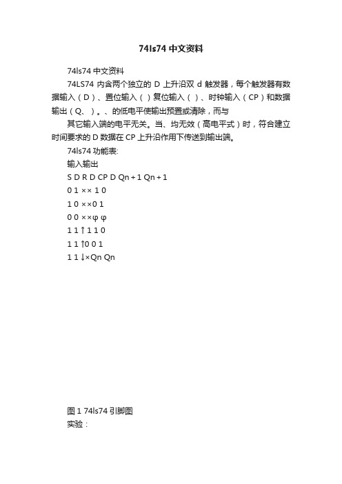
74ls74功能表:输入输出S D R D CP D Qn+1 Qn+10 1 ×× 1 01 0 ××0 10 0 ××φ φ1 1 ↑ 1 1 01 1 ↑0 0 11 1 ↓×Qn Qn图1 74ls74引脚图实验:用74LS74构成4位寄存器一个D触发器可实现一位二进数的存储,因此应采用4个D触发器实现4位寄存器。
由于要实现移位寄存,4个D触发器之间应相互联接。
(1)首先在图2中完成相应的联线,构成可实现并入并出、串入串出、并入串出、串入并出的多功能移位寄存。
按图接好电路。
(2) D3 D2 D1 D0分别接逻辑开关,Q3 Q2 Q1 Q0接发光二极管;(3) 先清零;(4) 按下列要求,实现相应功能,观察结果,并描述工作过程。
并入并出:使数据输入端D3D2D1D0=1011,给CP端输入一个正单脉冲,观察Q3Q2Q1Q0发光二极管的状态,、将结果填入表中。
并入串出:使数据输入端D3D2D1D0=1011,给CP端输入4个正单脉冲,观察Q3端发光二极管的状态,将结果填入表6中。
串入并出:使数据输入端D0分别为1011,同时通过给CP端输入正单脉冲将D0端的4 个数据送入寄存器。
观察Q3Q2Q1Q0端发光二极管的状态,将结果填入表中。
串入串出:使数据输入端D0分别为1011,同时通过给CP端输入正单脉冲,将D0端的4 个数据送入寄存器。
在CP端输完8个脉冲后,观察Q3端发光二极管的状态,将结果填入表2中。
并入并出:D3D2D1D0=10111个CP脉冲Q3Q2Q1Q0=结论:并入串出D3D2D1D0=10114个CP脉冲Q3=结论串入并出D3=10114个CP脉冲Q3Q2Q1Q0=结论串入串出D3=10118个CP脉冲Q3=结论图274ls153芯片管脚图引脚逻辑功能以及封装2007年12月17日 23:53 本站原创作者:本站用户评论()关键字:74ls153管脚图逻辑功能图封装:74LS163引脚功能表及管脚定义图(带时序波形图)发布:2011-08-30 | 作者: | 来源: huangjiapeng| 查看:2620次 | 用户关注:定时器由与系统秒脉冲(由时钟脉冲产生器提供)同步的计数器构成,要求计数器在状态信号ST作用下,首先清零,然后在时钟脉冲上升沿作用下,计数器从零开始进行增1计数,向控制器提供模5的定时信号TY和模25的定时信号TL。
- 1、下载文档前请自行甄别文档内容的完整性,平台不提供额外的编辑、内容补充、找答案等附加服务。
- 2、"仅部分预览"的文档,不可在线预览部分如存在完整性等问题,可反馈申请退款(可完整预览的文档不适用该条件!)。
- 3、如文档侵犯您的权益,请联系客服反馈,我们会尽快为您处理(人工客服工作时间:9:00-18:30)。
Copyright © 1988, Texas Instruments Incorporated PRODUCTION DATA information is current as of publication date.
Products conform to specifications per the terms of Texas Instruments
standard warranty. Production processing does not necessarily include
testing of all parameters.
1
POST OFFICE BOX 655303 • DALLAS, TEXAS 75265
2POST OFFICE BOX 655303 • DALLAS, TEXAS 75265
3 POST OFFICE BOX 655303 • DALLAS, TEXAS 75265
元器件交易网
IMPORTANT NOTICE
Texas Instruments and its subsidiaries (TI) reserve the right to make changes to their products or to discontinue
any product or service without notice, and advise customers to obtain the latest version of relevant information
to verify, before placing orders, that information being relied on is current and complete. All products are sold
subject to the terms and conditions of sale supplied at the time of order acknowledgement, including those
pertaining to warranty, patent infringement, and limitation of liability.
TI warrants performance of its semiconductor products to the specifications applicable at the time of sale in
accordance with TI’s standard warranty. Testing and other quality control techniques are utilized to the extent
TI deems necessary to support this warranty. Specific testing of all parameters of each device is not necessarily
performed, except those mandated by government requirements.
CERTAIN APPLICATIONS USING SEMICONDUCTOR PRODUCTS MAY INVOLVE POTENTIAL RISKS OF
DEATH, PERSONAL INJURY, OR SEVERE PROPERTY OR ENVIRONMENTAL DAMAGE (“CRITICAL
APPLICATIONS”). TI SEMICONDUCTOR PRODUCTS ARE NOT DESIGNED, AUTHORIZED, OR
WARRANTED TO BE SUITABLE FOR USE IN LIFE-SUPPORT DEVICES OR SYSTEMS OR OTHER
CRITICAL APPLICATIONS. INCLUSION OF TI PRODUCTS IN SUCH APPLICATIONS IS UNDERSTOOD TO
BE FULLY AT THE CUSTOMER’S RISK.
In order to minimize risks associated with the customer’s applications, adequate design and operating
safeguards must be provided by the customer to minimize inherent or procedural hazards.
TI assumes no liability for applications assistance or customer product design. TI does not warrant or represent
that any license, either express or implied, is granted under any patent right, copyright, mask work right, or other
intellectual property right of TI covering or relating to any combination, machine, or process in which such
semiconductor products or services might be or are used. TI’s publication of information regarding any third
party’s products or services does not constitute TI’s approval, warranty or endorsement thereof.
Copyright © 1999, Texas Instruments Incorporated。