美国赌城房价暴跌75%,30万美元以9.5万的跳楼价转手
2017初中英语单词、短语、词组汇总(C开头)

2017初中英语单词、短语、词组汇总(C开头)2017鍒濅腑鑻辫鍗曡瘝銆佺煭璇€佽瘝缁勬眹鎬伙紙C寮€澶达級C cabbage n. 鍗峰績鑿滐紝娲嬬櫧鑿?cafe n. 鍜栧暋棣嗭紱椁愰cage n 绗硷紱楦熺cake n. 铔嬬硶锛岀硶鐐癸紱楗?call n. 鍠婏紝鍙紱鐢佃瘽锛岄€氳瘽v. 绉板懠锛涘懠鍞わ紱鍠婏紝鍙?camel n. 楠嗛┘camera n. 鐓х浉鏈猴紱鎽勫儚鏈?camp n. 锛堝浠わ級钀?vi. 閲庤惀锛?瀹胯惀can1 (could) can't = can not modal v. 鍙兘锛涜兘澶燂紱鍙互涓嶈兘can2 缃愬ご锛涚綈瀛?Canada* n. 鍔犳嬁澶?Canadian a. 鍔犳嬁澶х殑锛涘姞鎷垮ぇ浜虹殑n. 鍔犳嬁澶т汉cancel vt. 鍙栨秷cancer n. 鐧?candle n. 铚$儧candy n. 绯栨灉cap n.锛堟棤妾愮殑鎴栦粎鍦ㄥ墠闈㈡湁妾愮殑锛夊附瀛愶紱锛堢摱瀛愮殑锛夌洊锛涳紙閽㈢瑪绛夌殑锛夌瑪濂?capital n. 棣栭兘锛岀渷浼氾紱澶у啓锛涜祫鏈?captain n. 锛堟捣鍐涳級涓婃牎锛涜埞闀匡紝鑸伴暱锛涢槦闀?car n. 姹借溅锛屽皬鍗ц溅card n. 鍗$墖锛涘悕鐗囷紱绾哥墝care n. 鐓ф枡锛屼繚鎶わ紱灏忓績v. 浠嬫剰鈥︼紝鍦ㄤ箮锛涘叧蹇?careful a. 灏忓績鐨勶紝浠旂粏鐨勶紝璋ㄦ厧鐨?careless a. 绮楀績鐨勶紝婕笉缁忓績鐨?carry vt. 鎷匡紝鎼紝甯︼紝鎻愶紝鎶紝鑳岋紝鎶憋紝杩愮瓑cartoon n. 鍔ㄧ敾鐗囷紝鍗¢€氾紱婕敾cat n. 鐚?锟斤拷catch (caught, caught) v. 鎺ヤ綇锛涙崏浣忥紱璧朵笂锛涙煋涓婏紙鐤剧梾锛?cause n. 鍘熷洜锛岃捣鍥?vt. 淇冧娇锛屽紩璧凤紝浣垮彂鐢?CD鍏夌洏(compact disk鐨勭缉鍐? CD ROM淇℃伅鍌ㄥ瓨鍏夌洏(compact disk read only memory鐨勭缉鍐? ceiling n. 澶╄姳鏉匡紝椤舵celebrate v. 搴嗙celebration n. 搴嗙锛涘簡绁濅細cent n. 缇庡垎锛?00 cents = 1 dollar 锛?central a. 涓績鐨勶紝涓ぎ鐨勶紱涓昏鐨?centre (缇?center ) n. 涓績锛屼腑澶?century n. 涓栫邯锛岀櫨骞?certain a. 锛堟湭鎸囨槑鐪熷疄鍚嶇О鐨勶級鏌愨€?纭畾鐨勶紝鏃犵枒鐨勶紱涓€瀹氫細鈥?certainly ad. 褰撶劧锛屾槸鐨勶紱涓€瀹氾紝鏃犵枒chair n. 妞呭瓙chairman n. 涓诲腑锛屼細闀匡紱璁暱chairwoman n. 濂充富甯?濂充細闀?濂宠闀?chalk n. 绮夌瑪challenge n.鎸戞垬(鎬? challenging a.鍏锋湁鎸戞垬鎬х殑champion n. 鍐犲啗锛屼紭鑳滆€?chance n. 鏈轰細锛屽彲鑳芥€?changeable a.鏄撳彉鐨勶紝鍙樺寲鏃犲父鐨?change n. 闆堕挶锛涙壘澶磛. 鏀瑰彉锛屽彉鍖栵紱鏇存崲锛涘厬鎹?chat n. & vi. 鑱婂ぉ锛岄棽璋?cheap a. 渚垮疁鐨勶紝璐?cheat n. & v. 楠楀彇锛屽搫楠楋紱浣滃紛check n. 妫€鏌ワ紱鎵规敼vt. 鏍″锛屾牳瀵癸紱妫€鏌ワ紱鎵规敼cheer n. & vi.锟斤拷娆㈠懠锛?鍠濆僵Cheer up鎸綔璧锋潵锛佹彁璧风簿绁烇紒cheerful a.鍏撮珮閲囩儓鐨勶紝蹇椿鐨?cheese n. 濂堕叒chemical a. 鍖栧鐨?n. 鍖栧鍝?chemist n. 鑽墏甯堬紱鍖栧瀹?chemistry n. 鍖栧cheque (缇巆heck) n. 鏀エchess n. 妫?chest n. 绠卞瓙锛涚洅瀛愶紱鑳搁儴chick n. 灏忛浮chicken n. 楦★紱楦¤倝child (澶峜hildren) n. 瀛╁瓙锛屽効绔?chimney n. 鐑熷洷锛岀儫绛?China* n. 涓浗Chinese a. 涓浗鐨勶紱涓浗浜虹殑锛涗腑鍥借瘽鐨勶紝姹夎鐨刵. 涓浗浜猴紱涓浗璇濓紝姹夎锛屼腑鏂?chips n. (pl.)鐐稿湡璞嗘潯锛堢墖锛?chocolate n. 宸у厠鍔?choice n. 閫夋嫨锛涙妷鎷?choose (chose, chosen) vt. 閫夋嫨chopsticks n. 绛峰瓙Christian n. 鍩虹潱鍜屽ぉ涓绘暀寰掔殑鎬荤ОChristmas n. 鍦h癁鑺傦紙12鏈?5鏃ワ級Christmas card鍦h癁鍗?Christmas tree鍦h癁鏍?Christmas Eve 鍦h癁锛堝墠锛夊church n. 鏁欏爞锛涙暀浼?cigarette n. 绾哥儫锛岄鐑?cinema n. 鐢靛奖闄紱鐢靛奖circle n. vt. 鍦嗗湀灏嗏€﹀湀璧锋潵citizen n. 鍏皯锛涘眳姘?city n. 甯傦紝鍩庡競锛岄兘甯?clap vi. 鎷嶆墜锛?榧撴帉class n. 锛堝鏍¢噷鐨勶級鐝紱骞寸骇锛涜classical a. 浼犵粺鐨勶紱鍙ゅ吀鐨?classmate n. 鍚岀彮鍚屽classroom n. 鏁欏clean vt. 寮勫共鍑€锛屾摝骞插噣a. 娓呮磥鐨勶紝骞插噣鐨?cleaner n. 娓呮磥宸ワ紱娓呮磥鍣紱娓呮磥鍓?clear a. 娓呮櫚鐨勶紱鏄庝寒鐨勶紱娓呮鐨?clearly ad. 娓呮鍦帮紝鏃犵枒鍦?clever a. 鑱槑鐨勶紝浼朵繍鐨?climb v. 鐖紝鏀€鐧?clinic n. 璇婃墍clock n. 閽?clone n. 鍏嬮殕锛堟棤鎬х箒娈栧嚭鏉ョ殑鏈夋満浣撶兢锛?close1 a. 浜插瘑鐨勶紱杩戯紝闈犺繎ad. 杩戯紝闈犺繎close2 vt. 鍏筹紝鍏抽棴cloth n. 甯?clothes n. 琛f湇锛涘悇绉嶈。
电缆规格型号代表的含义

型号含义:R-连接用软电缆(电线),软结构。
V-绝缘聚氯乙烯。
V-聚氯乙烯绝缘V-聚氯乙烯护套B-平型(扁形)。
S-双绞型。
A-镀锡或镀银。
F-耐高温P-编织屏蔽P2-铜带屏蔽P22-钢带铠装Y—预制型、一般省略,或聚烯烃护套FD—产品类别代号,指分支电缆。
将要颁布的建设部标准用FZ表示,其实质相同YJ—交联聚乙烯绝缘V—聚氯乙烯绝缘或护套ZR—阻燃型NH—耐火型WDZ—无卤低烟阻燃型WDN—无卤低烟耐火型例如:SYV 75-5-1(A、B、C)S: 射频Y:聚乙烯绝缘V:聚氯乙烯护套A:64编B:96编C:128编75:75欧姆5:线径为5MM 1:代表单芯SYWV 75-5-1S: 射频Y:聚乙烯绝缘W:物理发泡V:聚氯乙烯护套75:75欧姆5:线缆外径为5MM 1:代表单芯例如:RVVP2*32/0.2 RVV2*1.0 BVRR: 软线VV:双层护套线P屏蔽2:2芯多股线32:每芯有32根铜丝0.2:每根铜丝直径为0.2MM ZR-RVS2*24/0.12ZR: 阻燃R: 软线S:双绞线2:2芯多股线24:每芯有24根铜丝0.12:每根铜丝直径为0.12MM 型号、名称RV 铜芯氯乙烯绝缘连接电缆(电线)AVR 镀锡铜芯聚乙烯绝缘平型连接软电缆(电线)RVB 铜芯聚氯乙烯平型连接电线RVS 铜芯聚氯乙烯绞型连接电线RVV 铜芯聚氯乙烯绝缘聚氯乙烯护套圆形连接软电缆ARVV 镀锡铜芯聚氯乙烯绝缘聚氯乙烯护套平形连接软电缆RVVB 铜芯聚氯乙烯绝缘聚氯乙烯护套平形连接软电缆RV-105 铜芯耐热105oC聚氯乙烯绝缘聚氯乙烯绝缘连接软电缆AF-205AFS-250AFP-250 镀银聚氯乙氟塑料绝缘耐高温-60oC~250oC连接软电线2、规格表示法的含义规格采用芯数、标称截面和电压等级表示①单芯分支电缆规格表示法:同一回路电缆根数*(1*标称截面),0.6/1KV,如:4*(1*185)+1*95 0.6/1KV②多芯绞合型分支电缆规格表示法:同一回路电缆根数*标称截面,0.6/1KV,如:4**185+1*95 0.6/1KV③多芯同护套型分支电缆规格表示法:电缆芯数×标称截面-T,如:4×25-T一米3*150+1*95带铠国标铜电缆含多少铜?3*150+1*95=540平方毫米=5.4平方毫米1米=100厘米100*5.4*8.9=4806克=4.806公斤8.9是铜的比重常见电线电缆的规格型号BVVB:铜芯聚氯乙烯绝缘聚氯乙烯护套扁形(B)电线AVR:铜芯聚氯乙烯绝缘安装(A)用软(R)电线RV:软铜导体无护套电缆AVRB :铜芯聚氯乙烯绝缘扁形安装用软电线RVB:软铜导体扁形无护套电缆RVS:铜芯聚氯乙烯绝缘绞型(S)连接用软电线RVV:铜芯聚氯乙烯绝缘聚氯乙烯护套软电线(前一个V表示聚氯乙烯绝缘,后一个V表示聚氯乙烯护套)AVVR:铜芯聚氯乙烯绝缘聚氯乙烯护套安装用软电缆至于规格有3等芯4等芯和3+1 3个常用规格等芯就是截面一样的3+1就是地线的截面是相线的一半。
台湾75毛豆的栽培技术

松脆 , 糯性 强 , 口感好 , 济效益 高 , 合 作为 出 口蔬 经 适
菜 种植 。 2 栽培技 术
2 1 育 苗 移 栽 .
春季 毛 豆 可 采 用 育 苗 移 栽 ,本 地 一 般 在 3月
治 。豆荚 期 的病 虫 害 防治 主要 在前 期 幼 荚期 , 在鼓
台湾 7 5毛 豆株 型 挺 立 , 高 5  ̄ 0 m, 育期 株 06e 生 8  ̄ 5 , 枝强 , 均有效 分枝 45个 。叶卵 圆形 , 5 9d分 平 . 花 白色 , 青荚 深绿色 , 系发达 , 易倒 伏 , 根 不 耐肥水 。每
1  ̄ 5日,地温达 到 1  ̄ 2C 播 种 。 苗床 畦 面 宽 01 0 1  ̄时
荚 期避 免 用 药 。 害有 大 豆 食 心 虫 、 豆斜 纹 夜 蛾 虫 大
等 , 用 美 满 防 治 ; 害 主要 有 霜 霉 病 , 用 达 科 可 病 可 宁 或 金 雷 多 米尔 防治 。
10m, 墒高垄 , 到排灌 及 时 , 面耙 细耙 平 。晴 3c 深 做 畦 天足墒 播种 , 播种要 均匀 , 覆盖 细土 , 并 小拱 棚保 温 ,
33 病 虫 害 防 治 .
1 品种 特性
毛 豆 苗 期 的 主要 虫 害 有 大 豆卷 叶螟 、 豆蚜 、 菜
青 虫 等 ,发 现 初 孵 卵 幼 虫 时 用 抑 太保 10  ̄ 5 0 0 0 10 倍 液 均 匀 喷 雾 防治 , 虫 用 吡 虫 啉 1 0 液 喷 雾 蚜 5 0倍 防 治 ; 害 主 要 有 立 枯 病 、 病 , 病 发 初 期 用 达 病 锈 在 科 宁或 甲基 托 布 津 防 治 。 花 荚期 虫 害 主要 有 豆荚 螟 及 大豆 潜 叶蝇 等 ,可 用 美 满 在 虫 卵 孵 化 高 峰至 幼虫 期 防治 ; 害 主要 有 灰 斑 病 、 斑病 及 细 菌性 病 紫 角斑 病 等 ,可 用 甲基 托 布津 、达 科 宁 均 匀 喷雾 防
ELESA+GANTER德国制造GANTER叉形接头GN 751与叉形头DIN 71752

叉形接头 叉形头GN 751 DIN 71752technical informations 镀锌钢,蓝钝处理。
弹簧钢制,经硬化与回火处理,镀锌,蓝钝处理。
GN751型叉形接头由一个DIN71752型叉形头构成。
- B 型:装有带搭锁弹簧的叉形销。
- KL 型:装有KL 安全轴环。
材料安全轴环安装- SL型:装有SL安全轴环。
可提供的其它标准型号- L型:带左旋螺纹的销孔(d2)。
- F型:带细螺纹的销孔(d2)。
特征及应用叉形接头GN 751包含一个符合DIN 71752标准的叉形头和一个带安全轴环的接头销(KL型和SL型)或一枚搭锁弹簧(B型)。
所有款式的拆卸均无需工具和监视器。
根据DIN标准,尺寸d1=12带M12X1,5的细螺纹。
在实际应用中,对于该尺寸M12X1,25为首选规格。
DIN标准并未预计到d1=20的情况。
标准件主尺寸重量无销全套型号型号d1 H9/h11l1d2a b d3l2l3l4g DIN 71752-4-8-M4GN 751-4-8-M4-KL48M4848162165 DIN 71752-4-8-M4-*GN 751-4-8-M4-SL-*48M4848162165 DIN 71752-4-16-M4GN 751-4-16-M4-KL416M4848162466 DIN 71752-4-16-M4GN 751-4-16-M4-SL416M4848162466 DIN 71752-5-10-M5GN 751-5-10-M5-KL510M5105920267.59 DIN 71752-5-10-M5GN 751-5-10-M5-B510M5105920267.510 DIN 71752-5-10-M5GN 751-5-10-M5-SL510M5105920267.59 DIN 71752-5-10-M5L GN 751-5-10-M5L-KL510M5L105920267.510 DIN 71752-5-10-M5L GN 751-5-10-M5L-B510M5L105920267.510 DIN 71752-5-10-M5L GN 751-5-10-M5L-SL510M5L105920267.510 DIN 71752-5-20-M5GN 751-5-20-M5-KL520M5105930367.519 DIN 71752-5-20-M5GN 751-5-20-M5-B520M5105930367.515 DIN 71752-5-20-M5GN 751-5-20-M5-SL520M5105930367.519 DIN 71752-5-20-M5L GN 751-5-20-M5L-KL520M5L105930367.519 DIN 71752-5-20-M5L GN 751-5-20-M5L-B520M5L105930367.515 DIN 71752-5-20-M5L GN 751-5-20-M5L-SL520M5L105930367.519 DIN 71752-6-12-M6GN 751-6-12-M6-KL612M6126102431920 DIN 71752-6-12-M6GN 751-6-12-M6-B612M6126102431920 DIN 71752-6-12-M6GN 751-6-12-M6-SL612M6126102431920 DIN 71752-6-12-M6L GN 751-6-12-M6L-KL612M6L126102431920 DIN 71752-6-12-M6L GN 751-6-12-M6L-B612M6L 126102431920 DIN 71752-6-12-M6L GN 751-6-12-M6L-SL612M6L126102431920 DIN 71752-6-24-M6GN 751-6-24-M6-KL624M6126103643920 DIN 71752-6-24-M6GN 751-6-24-M6-B624M6126103643925 DIN 71752-6-24-M6GN 751-6-24-M6-SL624M6126103643920 DIN 71752-6-24-M6L GN 751-6-24-M6L-KL624M6L126103643920 DIN 71752-6-24-M6L GN 751-6-24-M6L-B624M6L126103643925 DIN 71752-6-24-M6L GN 751-6-24-M6L-SL624M6L126103643920 DIN 71752-8-16-M8GN 751-8-16-M8-KL816M81681432421245 DIN 71752-8-16-M8GN 751-8-16-M8-B816M81681432421250DIN 71752-8-16-M8GN 751-8-16-M8-SL816M81681432421245 DIN 71752-8-16-M8F GN 751-8-16-M8F-KL816M8F=M8x11681432421245 DIN 71752-8-16-M8F GN 751-8-16-M8F-B816M8F=M8x11681432421250 DIN 71752-8-16-M8F GN 751-8-16-M8F-SL816M8F=M8x11681432421245 DIN 71752-8-16-M8L GN 751-8-16-M8L-KL816M8L1681432421245 DIN 71752-8-16-M8L GN 751-8-16-M8L-B816M8L1681432421250 DIN 71752-8-16-M8L GN 751-8-16-M8L-SL816M8L1681432421245 DIN 71752-8-32-M8GN 751-8-32-M8-KL832M81681448581260 DIN 71752-8-32-M8GN 751-8-32-M8-B832M81681448581265 DIN 71752-8-32-M8DIN 751-8-32-M8-SL832M81681448581260 DIN 71752-8-32-M8F GN 751-8-32-M8F-KL832M8F=M8x11681448581260 DIN 71752-8-32-M8F GN 751-8-32-M8F-B832M8F=M8x11681448581265 DIN 71752-8-32-M8F GN 751-8-32-M8F-SL832M8F=M8x11681448581260 DIN 71752-8-32-M8L GN 751-8-32-M8L-KL832M8L1681448581265 DIN 71752-8-32-M8L GN 751-8-32-M8L-B832M8L1681448581265 DIN 71752-8-32-M8L GN 751-8-32-M8L-SL832M8L1681448581265 DIN 71752-10-20-M10GN 751-10-20-M10-KL1020M1020101840521590 DIN 71752-10-20-M10GN 751-10-20-M10-B1020M1020101840521590 DIN 71752-10-20-M10GN 751-10-20-M10-SL1020M1020101840521590 DIN 71752-10-20-M10F GN 751-10-20-M10F-KL1020M10F=M10x1.2520101840601590 DIN 71752-10-20-M10F GN 751-10-20-M10F-B1020M10F=M10x1.2520101840521590 DIN 71752-10-20-M10F GN 751-10-20-M10F-SL1020M10F=M10x1.2520101840521590 DIN 71752-10-20-M10L GN 751-10-20-M10L-KL1020M10L20101840521590 DIN 71752-10-20-M10L GN 751-10-20-M10L-B1020M10L20101840521590 DIN 71752-10-20-M10L GN 751-10-20-M10L-SL1020M10L20101840521590 DIN 71752-10-40-M10GN 751-10-40-M10-KL1040M10201018607215120 DIN 71752-10-40-M10GN 751-10-40-M10-B1040M10201018607215120 DIN 71752-10-40-M10GN 751-10-40-M10-SL1040M10201018607215120 DIN 71752-10-40-M10F GN 751-10-40-M10F-KL1040M10F=M10x1.25201018607215120 DIN 71752-10-40-M10F GN 751-10-40-M10F-B1040M10F=M10x1.25201018607215120 DIN 71752-10-40-M10F GN 751-10-40-M10F-SL1020M10F=M10x1.2520101840601590 DIN 71752-10-40-M10L GN 751-10-40-M10L-KL1040M10L201018607215120 DIN 71752-10-40-M10L GN 751-10-40-M10L-B1040M10L201018607215120 DIN 71752-10-40-M10L GN 751-10-40-M10L-SL1040M10L201018607215120 DIN 71752-12-24-M12GN 751-12-24-M12-KL1224M12241220486218144 DIN 71752-12-24-M12GN 751-12-24-M12-B1224M12241220486218150 DIN 71752-12-24-M12GN 751-12-24-M12-SL1224M12241220486218144 DIN 71752-12-24-M12F GN 751-12-24-M12F-KL1224M12F=M12x1.25241220486218144 DIN 71752-12-24-M12F GN 751-12-24-M12F-B1224M12F=M12x1.25241220486218150 DIN 71752-12-24-M12F GN 751-12-24-M12F-SL1224M12F=M12x1.25241220486218144 DIN 71752-12-24-M12L GN 751-12-24-M12L-KL1224M12L241220486218144 DIN 71752-12-24-M12L GN 751-12-24-M12L-B1224M12L241220486218150 DIN 71752-12-24-M12L GN 751-12-24-M12L-SL1224M12L241220486218144 DIN 71752-12-48-M12GN 751-12-48-M12-KL1248M12241220728618192 DIN 71752-12-48-M12GN 751-12-48-M12-B1248M12241220728618200DIN 71752-12-48-M12GN 751-12-48-M12-SL1248M12241220728618192 DIN 71752-12-48-M12F GN 751-12-48-M12F-KL1248M12F=M12x1.25241220728618192 DIN 71752-12-48-M12F GN 751-12-48-M12F-B1248M12F=M12x1.25241220728618200 DIN 71752-12-48-M12F GN 751-12-48-M12F-SL1248M12F=M12x1.25241220728618192 DIN 71752-12-48-M12L GN 751-12-48-M12L-KL1248M12L241220728618192 DIN 71752-12-48-M12L GN 751-12-48-M12L-B1248M12L241220728618200 DIN 71752-14-28-M14GN 751-14-28-M14-SL1248M12L241220728618192 DIN 71752-14-28-M14GN 751-14-28-M14-KL1428M14271424567222.5220 DIN 71752-14-28-M14GN 751-14-28-M14-B1428M14271424567222.5218 DIN 71752-14-28-M14GN 751-14-28-M14-SL1428M14271424567222.5220 DIN 71752-14-28-M14F GN 751-14-28-M14F-KL1428M14F=M14x1.5271424567222.5220 DIN 71752-14-28-M14F GN 751-14-28-M14F-B1428M14F=M14x1.5271424567222.5218 DIN 71752-14-28-M14F GN 751-14-28-M14F-SL1428M14F=M14x1.5271424567222.5220 DIN 71752-14-28-M14L GN 751-14-28-M14L-KL1428M14L271424567222.5220 DIN 71752-14-28-M14L GN 751-14-28-M14L-B1428M14L271424657222.5218 DIN 71752-14-28-M14L GN 751-14-28-M14L-SL1428M14L271424567222.5220 DIN 71752-14-56-M14GN 751-14-56-M14-KL1456M142714248510122.5290 DIN 71752-14-56-M14GN 751-14-56-M14-B1456M142714248510122.5300 DIN 71752-14-56-M14GN 751-14-56-M14-SL1456M142714248510122.5290 DIN 71752-14-56-M14F GN 751-14-56-M14F-KL1458M14F=M14x1.52714248510122.5290 DIN 71752-14-56-M14F GN 751-14-56-M14F-B1456M14F=M14x1.52714248510122.5300 DIN 71752-14-56-M14F GN 751-14-56-M14F-SL1458M14F=M14x1.52714248510122.5290 DIN 71752-14-56-M14L GN 751-14-56-M14L-KL1456M14L2714248510122.5290 DIN 71752-14-56-M14L GN 751-14-56-M14L-B1456M14L2714248510122.5300 DIN 71752-14-56-M14L GN 751-14-56-M14L-SL1456M14L2714248510122.5290 DIN 71752-16-32-M16GN 751-16-32-M16-KL1632M16321626648324335 DIN 71752-16-32-M16GN 751-16-32-M16-B1632M16321626648324340 DIN 71752-16-32-M16GN 751-16-32-M16-SL1632M16321626648324335 DIN 71752-16-32-M16F GN 751-16-32-M16F-KL1632M16F=M16x1.5321626648324335 DIN 71752-16-32-M16F GN 751-16-32-M16F-B1632M16F=M16x1.5321626648324340 DIN 71752-16-32-M16F GN 751-16-32-M16F-SL1632M16F=M16x1.5321626648324335 DIN 71752-16-32-M16L GN 751-16-32-M16L-KL1632M16L321626648324335 DIN 71752-16-32-M16L GN 751-16-32-M16L-B1632M16L321626648324340 DIN 71752-16-32-M16L GN 751-16-32-M16L-SL1632M16L321626648324335 DIN 71752-16-64-M16GN 751-16-64-M16-KL1664M163216266411524470 DIN 71752-16-64-M16GN 751-16-64-M16-B1664M163216269611524460 DIN 71752-16-64-M16GN 751-16-64-M16-SL1664M163216266411524470 DIN 71752-16-64-M16F GN 751-16-64-M16F-KL1664M16F=M16x1.53216269611524470 DIN 71752-16-64-M16F GN 751-16-64-M16F-B1664M16F=M16x1.53216649611524460 DIN 71752-16-64-M16F GN 751-16-64-M16F-SL1664M16F=M16x1.53216269611524470 DIN 71752-16-64-M16L GN 751-16-64-M16L-A1664M16L3216269611524470 DIN 71752-16-64-M16L GN 751-16-64-M16L-B1664M16L3216269611524460 DIN 71752-16-64-M16L GN 751-16-64-M16L-SL1664M16L3216269611524470 DIN 71752-20-40-M20GN 751-20-40-M20-KL2040M204020348010530800。
P75NE75

STP75NE75STP75NE75FPN -CHANNEL 75V -0.01Ω-75A TO-220/TO-220FPSTripFET ™POWER MOSFETs TYPICAL R DS(on)=0.01Ωs EXCEPTIONAL dv/dt CAPABILITY s 100%AVALANCHE TESTED sAPPLICATION ORIENTED CHARACTERIZATIONDESCRIPTIONThis Power MOSFET is the latest development of STMicroelectronics unique ”Single Feature Size ™”strip-based process.The resulting transi-stor shows extremely high packing density for low on-resistance,rugged avalanche characteristics and less critical alignment steps therefore a re-markable manufacturing reproducibility.APPLICATIONSs SOLENOID AND RELAY DRIVERSs DC MOTOR CONTROL,AUDIO AMPLIFIERS s DC-DC CONVERTERSs AUTOMOTIVE ENVIRONMENT®INTERNAL SCHEMATIC DIAGRAMABSOLUTE MAXIMUM RATINGSSymbol ParameterValueUnit STP75NE75STP75NE75FP V DS Drain-source Voltage (V GS =0)75V V DGR Drain-gate Voltage (R GS =20k Ω)75VV GS Gate-source Voltage±20V I D Drain Current (continuous)at T c =25o C 7540A I D Drain Current (continuous)at T c =100o C 5328A I DM (•)Drain Current (pulsed)300160A P tot Total Dissipation at T c =25oC 16050W Derating Factor1.060.37W/o C V ISO Insulation Withstand Voltage (DC)2000V dv/dt Peak Diode Recovery voltage slope 7V/nsT s tg Storage Temperature-65to 175o C T j Max.Operating Junction Temperature175oC (•)Pulse width limited by safe operating area(1)I SD ≤75A,di/dt ≤300A/µs,V DD ≤V (BR)DSS ,T j ≤T JMAXTYPE V DSS R DS(on)I D STP75NE75STP75NE75FP75V 75V<0.013Ω<0.013Ω75A 40AMay 1999TO-220TO-220FP1231231/9THERMAL DATATO-220TO-220FPR thj-case Thermal Resistance Junction-case Max0.94 2.7o C/WR thj-amb R thc-sinkT l Thermal Resistance Junction-ambient MaxThermal Resistance Case-sink TypMaximum Lead Temperature For Soldering Purpose62.50.5300o C/Wo C/Wo CAVALANCHE CHARACTERISTICSSymbol Parameter Max Value UnitI AR Avalanche Current,Repetitive or Not-Repetitive(pulse width limited by T j max)75AE AS Single Pulse Avalanche Energy(starting T j=25o C,I D=I AR,V DD=30V)200mJELECTRICAL CHARACTERISTICS(T case=25o C unless otherwise specified)OFFSymbol Parameter Test Conditions Min.Typ.Max.Unit V(BR)DSS Drain-sourceBreakdown VoltageI D=250µA V GS=075VI DSS Zero Gate VoltageDrain Current(V GS=0)V DS=Max RatingV DS=Max Rating T c=125o C110µAµAI GSS Gate-body LeakageCurrent(V DS=0)V GS=±20V±100nA ON(∗)Symbol Parameter Test Conditions Min.Typ.Max.Unit V GS(th)Gate Threshold Voltage V DS=V GS I D=250µA234V R DS(on)Static Drain-source OnResistanceV GS=10V I D=37.5A0.010.013ΩI D(o n)On State Drain Current V DS>I D(o n)x R DS(on)ma xV GS=10V75A DYNAMICSymbol Parameter Test Conditions Min.Typ.Max.Unitg f s(∗)ForwardTransconductanceV DS>I D(o n)x R DS(on)ma x I D=37.5A40SC iss C os s C rss Input CapacitanceOutput CapacitanceReverse TransferCapacitanceV DS=25V f=1MHz V GS=05300850310pFpFpFSTP75NE75/FP 2/9ELECTRICAL CHARACTERISTICS(continued)SWITCHING ONSymbol Parameter Test Conditions Min.Typ.Max.Unitt d(on) t r Turn-on Delay TimeRise TimeV DD=40V I D=40AR G=4.7 ΩV GS=10V(Resistive Load,see fig.3)32130nsnsQ g Q gs Q gd Total Gate ChargeGate-Source ChargeGate-Drain ChargeV DD=60V I D=75A V GS=10V1503062200nCnCnCSWITCHING OFFSymbol Parameter Test Conditions Min.Typ.Max.Unitt d(of f) t f Turn-off Delay TimeFall TimeV DD=40V I D=40AR G=4.7 ΩV GS=10V(Resistive Load,see fig.3)15045nsnst r(Voff) t f t c Off-voltage Rise TimeFall TimeCross-over TimeV clamp=60V I D=75AR G=4.7 ΩV GS=4.5V(Inductive Load,see fig.5)3560100nsnsnsSOURCE DRAIN DIODESymbol Parameter Test Conditions Min.Typ.Max.UnitI SD I SDM(•)Source-drain CurrentSource-drain Current(pulsed)43170AAV SD(∗)Forward On Voltage I SD=75A V GS=0 1.5Vt rr Q rr I RRM Reverse RecoveryTimeReverse RecoveryChargeReverse RecoveryCurrentI SD=75A di/dt=100A/µsV DD=30V T j=150o C(see test circuit,fig.5)1300.69nsµCA(∗)Pulsed:Pulse duration=300µs,duty cycle1.5%(•)Pulse width limited by safe operating areaSafe Operating Area for TO-220Safe Operating Area for TO-220FPSTP75NE75/FP3/9Thermal Impedance for TO-220 Output Characteristics Transconductance Thermal Impedance forTO-220FP Transfer CharacteristicsStatic Drain-source On ResistanceSTP75NE75/FP 4/9Gate Charge vs Gate-source Voltage Normalized Gate Threshold Voltage vs TemperatureSource-drain Diode Forward Characteristics Capacitance VariationsNormalized On Resistance vs TemperatureSTP75NE75/FP5/9Fig.1:Unclamped Inductive Load Test Circuit Fig.3:Switching Times Test Circuits For Resistive Load Fig.2:Unclamped Inductive Waveform Fig.4:Gate Charge test CircuitFig.5:Test Circuit For Inductive Load Switching And Diode Recovery TimesSTP75NE75/FP6/9DIM.mminch MIN.TYP.MAX.MIN.TYP.MAX.A 4.40 4.600.1730.181C 1.23 1.320.0480.051D 2.402.720.0940.107D1 1.270.050E 0.490.700.0190.027F 0.610.880.0240.034F1 1.14 1.700.0440.067F2 1.14 1.700.0440.067G 4.95 5.150.1940.203G1 2.4 2.70.0940.106H210.010.400.3930.409L216.40.645L413.014.00.5110.551L5 2.65 2.950.1040.116L615.2515.750.6000.620L7 6.2 6.60.2440.260L9 3.5 3.930.1370.154DIA.3.75 3.850.1470.151L6ACDED 1FGL7L2Dia.F 1L5L4H 2L9F 2G 1TO-220MECHANICAL DATAP011CSTP75NE75/FP7/9DIM.mm inch MIN.TYP.MAX.MIN.TYP.MAX.A 4.4 4.60.1730.181B 2.5 2.70.0980.106D 2.5 2.750.0980.108E 0.450.70.0170.027F 0.7510.0300.039F1 1.15 1.70.0450.067F2 1.15 1.70.0450.067G 4.95 5.20.1950.204G1 2.4 2.70.0940.106H 1010.40.3930.409L2160.630L328.630.6 1.126 1.204L49.810.60.3850.417L615.916.40.6260.645L799.30.3540.366Ø3 3.20.1180.126L2ABDEHGL6¯FL3G 1123F 2F 1L7L4TO-220FP MECHANICAL DATASTP75NE75/FP8/9Information furnished is believed to be accurate and reliable.However,STMicroelect r onics assumes no responsibility for the consequences of use of such information nor for any infringement of patents or other rights of third part i es which may result from its use.No license is granted by implication or otherwise under any patent or patent rights of STMicroelectro nics.Specification mentioned in this publication are subject to change without notice.This publication supersedes and replaces all informat i on previously supplied.STMicroelectronics products are not authorized for use as critical components in life support devices or systems with out express written approval of STMicroelectronics.The ST logo is a trademark of STMicroelectronics ©1999STMicroelectronics –Printed in Italy –All Rights ReservedSTMicroelectronics GROUP OF COMPANIESAustralia -Brazil -Canada -China -France -Germany -Italy -Japan -Korea -Malaysi a -Malta -Mexico -Morocco -The Netherlands -Singapore -Spain -Sweden -Switzerland -Taiwan -Thailand -United Kingdom -U.S.A..STP75NE75/FP9/9。
网络教学综合平台教师简明使用手册
安徽大学网络教学综合平台教师简明使用手册清华大学教育技术研究所2010 年02 月J lil 硼网络教学综合平台--教师用户简明使用手册图1-2平台登录首页(登录后点击“进入”按钮)教师首页”、课程教学” “精品课程”、和课程展示”第一部分登录系统第一步:登录网络教学综合平台如图所示:输入用户名和密码。
农卡胃"版盂It 強松WftJS ・Cl-dHf ・ 畫样軽軒哝期厦动■诜口貧哥林飙■母冉事,宙挣ii 诉诃推H ・T T rlR 平 iJ^TUtWlf*l»JWHTTR[ it 爭也工¥晴电于H 学禺強;t 序厦 讣!TF :科学与技*半隱RC¥ttHWSl£计.古羸霞鞏攻穆斗评罚童录議鲂乞+力建慳了■天的辛Ml 番* 工鼻址冏jsstieM ■纯.曲!(供丁览廿的曰主壬动功配.ffjtss Tilrar-#^if.H$L9KYT^畀利诗计琴診*■此"*ff1Wfirlift,忸是整出一 H 主"-ifrff灯说' 事丘比書怕理工制MF. 5F±*P±IS5iBft1T. *宦牯界辛主坯JSJtfJ 年TlH 力fte 可布■怔邛伺内L :■力杵握弋價的古式詮・样叮刊中. dn-KKliWBIhhdt*7T ■ ■■計 ・《 *1* 册,■ Ml HWf 血 E U W* 啬■Dp^^^on4 ■吕 urn*图1-1 访问网络教学综合平台登录系统后,继续点击“进入”按钮,进入平台,如下图所示页面。
»JE#■穴!E 套整甲J :査竹零决特辛,區丹岷讨■釈$摩垃*支片1•章创留.frtfjli.且三睾k,肉柞-马恵1;壬:t 厳出鸟再工mMdQ (DH1XB : 1 壬*则蓝:即鼻罔页面上方列出了四个导航栏,分别是:・欣注像用曲霰#峰齿3吃卜 «j |ig./ria n.m.■玄 1 Iff 昌伦即 | ltrF€# | E7N4JF . utt^ *1肯#叫r*K »SuH*4U«BtTf.5 st.-fS. £兀片主厅理弓貳十;事亡灯箱7.勺評岬If I 士丁響丁旳不贰岳讶ZAftFlfSFW 井ltftTlEfl-P*Pt3ttW tt^fiST«nfft2Hr'京E?聘用舸圧"¥蔺告:風络教学Mt ]号、冃「日互功辺Anciuici 円二勻s4个、整凋J MTiZ^ij&应申習询图1-4修改密码页面第二部分通用网络教学平台第一步:进入课程教学空间A *JT 妙 ffiti -fl 1H4撫学荷圧俵G E 掙亡祥4严莘甘芹 △曲咅ti 瞬住 CS Fl 上3;坛 'iftri*7FAwfflafl i 杠曲B 甲谓"忑星暉B 凸府珂百和宫丁1&=一读宦炜莒誓也也晦qgi 査H£律丼设弹甚盘看■逋亦|短正莊航覆I 门度轻耳亢鼻主丈两港皂济竿仃 迴J 輕[](« 删tftL 聊户)1尽0 「「『 敕攪妁课稈辱*2二岂配T 泊怙;齐土_|色<童!_(iitfr-rr ;TI = I图1-3进入系统之后的教师首页第二步:修改密码进入平台之后,您可以修改自己的密码。
VW75147_EN_2011-01-01

Wiring Harnesses in Motor VehiclesQuality Requirements for Products and ProcessesPrefaceDetailed requirements and procedures are stipulated in the Group Quality Assurance and Procure‐ment Guideline for the Wiring Harness Product Audit. All specifications apply to the condition of wiring harnesses upon delivery to the Volkswagen Group.Previous issuesVW 75147: 2005-11ChangesThe following changes have been made compared with VW 75147: 2005-11:–Standard restructured–Sections 3 and 4 revised–Referenced standards updatedContents PageScope .........................................................................................................................2General requirements (2)Wiring harness ASSY .................................................................................................3Marking/identification .................................................................................................3As-received condition .................................................................................................3Function tests .............................................................................................................3Electric test .................................................................................................................3Mechanical/visual test ................................................................................................4Leak tightness test .. (4)1233.13.23.33.3.13.3.23.3.3Group Standard VW 75147Issue 2011-01Class. No.:69343Descriptors:harness, wiring harness, line, cable,Verify that you have the latest issue of the Standard before relying on it.This electronically generated Standard is authentic and valid without signature.The English translation is believed to be accurate. In case of discrepancies, the German version is alone authoritative and controlling.Page 1 of 10Confidential. All rights reserved. No part of this document may be provided to third parties or reproduced without the prior consent of the Standards Department of a Volkswagen Group member.This Standard is available to contracting parties solely via the B2B supplier platform .© Volkswagen Aktiengesellschaft VWNORM-2010-08eTest table ...................................................................................................................4Components ...............................................................................................................4Contact elements .......................................................................................................4Contact range .............................................................................................................4Contact elements with open crimp sleeves ................................................................4Contact elements with closed crimp sleeve ...............................................................4Special designs ..........................................................................................................5Splice connectors (potential connectors) ...................................................................5Crimp connectors .......................................................................................................5Ultrasonic weld connector ..........................................................................................6Housing ......................................................................................................................7Unsealed ....................................................................................................................7Sealed ........................................................................................................................7Lines ...........................................................................................................................7Individual lines ............................................................................................................7Twisted lines ..............................................................................................................7Sheathed lines ...........................................................................................................7Special lines ...............................................................................................................7Windings ....................................................................................................................8Line protection ............................................................................................................8Cable ties ...................................................................................................................9Grommets ..................................................................................................................9Assembled grommets/boots .......................................................................................9Foamed grommets .....................................................................................................9Injection-molded grommets ........................................................................................9Cable guides ..............................................................................................................9Electrical threaded connections ...............................................................................10Other applicable documents ....................................................................................103.3.444.14.1.14.1.24.1.34.1.44.24.2.14.2.24.34.3.14.3.24.44.4.14.4.24.4.34.4.44.54.64.74.84.8.14.8.24.8.34.94.105ScopeThis standard defines quality requirements and tests for wiring harnesses in motor vehicles. It applies to all vehicle wiring harnesses manufactured in production.General requirementsOnly parts released by Volkswagen must be used.The standard must be applied during production by–all plants of Volkswagen AG and production locations of subsidiaries that produce wiring har‐nesses and build vehicles,–all external suppliers that manufacture corresponding products and supply to purchaser plantsof Volkswagen AG as well as their supplying manufacturing locations of the same corporate group, module/sub-suppliers, outsourced production and …extended workbenches“.To ensure the proper mechanical and electrical functioning of the electric system, all parts must comply with the valid specifications (drawings, Technical Supply Specifications, national, interna‐tional, and Volkswagen in-house standards) and the evaluation criteria of this standard as well as the Guideline for the Wiring Harness Product Audit (see B2B supplier platform, Quality Assurance).The use of parts which do not conform to the specification must be safeguarded by obtaining a de‐viation permit (AVON) and the written approval of the responsible electrical engineering department1 2 Page 2VW 75147: 2011-01(Organizational Directive OA 700/3). The general quantity limitation and/or periods of validity of de‐viation permits (AWE) (generally 90 days) must be taken into consideration in this respect.Wiring harness ASSY Marking/identificationWiring harnesses must be clearly labeled. The wiring harness labels must be designed and attached in accordance with the drawing specifications. The label must be legible and resistant to decompo‐sition for the entire life cycle of the vehicle. The scope of identification is stipulated in the drawings or the Performance Specifications. It must be possible to assign customer-specific wiring harnesses (KSK) clearly to the vehicle (e.g. using the code).As-received conditionIn the as-received condition, the wiring harness must not be damaged nor bent or rolled together in a manner that could influence its operation. This applies in particular to areas which include washer fluid hoses (see Section 4.3.2), antenna lines and optical fibers.The packaging must be coordinated with the purchaser plant.Handling optical fibers–When handling optical fibers the specifications according to VW 60539-1 must be observed.–The optical fiber must not be bent, i.e. bend radii lower than 25 mm are not permitted, and thismust be ensured by using appropriate holders during the production of the wiring harness and appropriate packaging.–Contact with, scratching or soiling of the end surfaces must be prevented using protective caps which are to be removed only during testing.–As optical fibers are sensitive to pinching (the signal quality decreases), pinching must be avoid‐ed.Function testsElectric test Manufactured wiring harnesses must be fully function tested.Additional requirements on the electrical function test:Wiring harnesses must be fully tested in the ASSY for polarity reversal, short-circuit, line interruption.A label, which is printed automatically after the OK test, or another appropriate compulsory marking,generally serves as proof of an OK test result (see Section 3.1).The primary lock of the contacts must be verified for housings without secondary lock. Closed sec‐ondary locks and push back are accepted proofs.Test labels are only printed out after the function test has been completed (with OK status). A new electrical function test is mandatory for all reworked parts before delivery.Each wiring harness must not be tested more often than three times on the electrical test table. If the third test still reveals errors, the affected wiring harness must be scrapped and a new one must be produced.33.1 3.2 3.3 3.3.1Page 3VW 75147: 2011-01Mechanical/visual testThe mechanical/visual test comprises the verification of component availability, identity and position as per wiring harness drawing. A wear-free check as to the straightness of contact pins up to 1,2 mm must be integrated in the test table module.Washing water piping/vacuum lines are generally inspected in the ASSY for their presence, passage,and for leak-tightness. The test is carried out with an air pressure of 500 kPA.Leak tightness testAll sealed housings must be subjected to a pressure test (leakage test).Test tableSprung measuring pins must be used for the connection on the test table. Their function (spring force)must be tested regularly as per manufacturer specifications. All functions must be ensured by regular test and maintenance works (electrical, latch test, leak tightness test).Components Contact elements Contact rangeAll contact elements must comply with the detail and standard parts drawings.The contact area must be free of defects.For all contact elements, the form and positional tolerances (release drawings) must be observed.Screwing surfaces of cable sockets must be even, free of burrs, without lettering or embossing.Contact elements with open crimp sleeves Crimp connections must be realized according to VW 60330.In general, proof of the required process capability must be furnished for all crimp variants during first sampling. Metallographic sections must be provided upon purchaser request.Wire/conductor crimpIn the case of double crimps, the parallel arrangement of both conductors is only permitted if it can be ensured that the insulation crimp encompasses both conductors equally.Sealed design with individual line sealThe crimp edges must hold the individual line seals securely in position.The individual line seal must not be damaged by the crimp.The end of the conductor insulation must be visible between the wire crimp and the seal.Contact elements with closed crimp sleeve See DIN EN 60352-2, downstream VW 60330 is valid.3.3.2 3.3.3 3.3.4 44.14.1.1 4.1.2 4.1.2.1 4.1.2.2 4.1.3 Page 4VW 75147: 2011-01Special designs Flat conductor connectorCrimping technologySpecified crimp heights are a critical quality feature. The correct positioning and alignment (X/Y axes)of crimp contacts must be observed.The instructions in the manufacturer’s test specifications must be observed.Laser brazing technologyThe instructions in the manufacturer’s test specifications must be observed.Penetration technology (flat conductor multi-crimp connections)Contact elements and housing must not be damaged by the crimping process. The instructions in the manufacturer’s test specifications must be observed.Splice connectors (potential connectors)Splice connectors must be designed as ultrasonic weld joint as per VW 60307 or as crimp connector as per VW 60330 and DIN EN 60352-2.Crimp connectorsThe splice and crimp connectors must be treated as contact elements. They are subject to technical engineering approval.The crimp connectors must be adjusted according to the entire conductor cross-section pressed intothem.The crimp must have an inlet and outlet bellmouth (see Figure 1).The cut-off tabs must not come into contact with the conductor insulations.Figure 14.1.44.1.4.1 4.1.4.1.1 4.1.4.1.2 4.1.4.1.3 4.2 4.2.1 Page 5VW 75147: 2011-01Unsealed designFor crimp splices, (unless otherwise specified product-specifically) the conductor ends must project a max. 3 mm axially from the nodes. The edge of the cut-off tab is used as the reference point.The insulation variants must comply with the drawings and standards. The splice connectors must be insulated with at least 3 layers of wrapping tape. The insulation must be centered and should extend at least 10 mm on both sides over the non-insulated areas. The insulation must be secured against moving and be completely sealed; it must not display any gaps.Sealed design Splice connectors in damp spaces must be made fully waterproof by means of a heat-shrinkable plastic tube according to TL 82324, which is fitted with an internal layer of thermoplastic adhesive.Only transparent labeled tubes must be used in order to make it possible to identify clearly the posi‐tioning and the type of heat shrink tubing.Water leak tightness must be tested during production with air pressure in the water bath and via the insulation resistance. In the case of splice connectors, the leak tightness must be proven for the relevant weld node configurations.Ultrasonic weld connectorUltrasonic weld connections must comply with VW 60307.The welding energy must not affect the contacts. This must be ensured by sufficient distance (at least 400 mm) or by appropriate damping methods.Copper strands oxidize and insulation material ages. Copper oxides and ageing residues may affect unfavorably the welding process. It might be impossible to process them with the set parameters.The storage time of pre-cut material waiting for release of the manufacturing process must not exceed 8 weeks. The insulation of the line is to be removed immediately before the welding.In symmetrical ultrasonic weld connectors, the intermixing of the individual wires must be ensured by using insertions tools.In the case of ultrasonic weld connections, the process capability must be proven for the relevant weld case.–During processing, the contamination of the conductor surfaces with impurities (e.g. sweat from hands, grease etc.) must be excluded by taking suitable measures.–Different conductor structures (fine wires with normal) must be released on a case-by-case basis (ABS).–For release by the supplier (production) the actual yard goods must be welded; production re‐leases must be documented.Unsealed design See Section 4.2.1.1.Sealed designSee Section 4.2.1.2.4.2.1.1 4.2.1.2 4.2.2 4.2.2.14.2.2.2 Page 6VW 75147: 2011-01Housing UnsealedPlug housings and all related latch elements must be completely and properly mounted and must not display any damage. Secondary locks must be closed in the wiring harness’ as-received condition.Contact parts must be properly locked in the plug housing chambers.Sealed The same requirements apply as in Section 4.3.1.All seals must be present in the plug housing.Sealing lips of the individual line seals must not project from the sealing channel and must not be damaged.All sealing lips of blind plugs must be positioned within the housing chamber of the plug housing after assembly and seal it (min. 1,0 mm to max. 3,0 mm).Lines Individual lines Individual lines must comply with the corresponding Volkswagen release drawings and are subject to technical engineering approval according to VW 60306.The line insulation must be free of defects.Lines and line insulation must not be damaged.All individual lines in the wiring harness ASSY must comply with the design specifications with respect to cross-section and feature the required color combination (basic color + code color).Twisted linesTwisted lines must comply with VW 75205 and are subject to technical engineering approval. Any existing reinforced twisting for protection against fraying is part of the technical engineering approval.In the case of twisted lines, the line ends must be untwisted. Target: (50 ± 20) mmBefore contacting, the twist at the line ends must be removed.Sheathed linesThe line insulation must be free of defects.Lines and line insulation must not be damaged.The insulation of the individual lines must not be torn or cut as a result of removing the sheath.Special lines Flexible flat cables according to VW 60553-1No delaminations, bubbles, bends, folds or waviness are permitted for flexible flat cables.4.34.3.1 4.3.2 4.44.4.1 4.4.2 4.4.3 4.4.44.4.4.1 Page 7VW 75147: 2011-01Films must not be cracked, the cover and base film must not be damaged (no holes or missing insulation material). The cut edges of the film must not display any damage or burr formation. Elec‐trical bridges between conductors and conductor breaks are not permitted.Film perforations must ensure good separability of branches, but there must not be any film separation however.The bend radius must not be less than the min. 0,5 mm for flexible flat cable harnesses, film folds (e.g. 90° branches) must generally be wrapped.Optical fibers according to VW 60539-1All connecting pieces and protective caps must be present on the optical fibers.Damage to the optical fiber sheath is not permitted.The specifications with respect to optical attenuation of an optical fiber equipped with ferrules must be observed. The requirements of the test level budget according to VW 60539-3 apply.The contact retention force of the ferrules on the optical fiber must be > 60 N.Scratched or soiled end surfaces of the optical fiber are not permitted.The optical fiber must not be bent, bending radii < 25 mm are not permitted.Attenuation must be tested before delivery of the wiring harness.No damage must occur when the end surfaces are being cleaned. Cleaning residues are not per‐missible.An attenuation test after cleaning is absolutely essential.Coaxial cablesIndividual lines are subject to technical engineering approval according to VW 75206-1.See LAH V03 825.Coaxial lines must not be bent and/or radially deformed.WindingsAdhesive tapes according to VW 60360-1 must be used for applications in the engine compartment.Adhesive tapes must be cut.Adhesive tapes are subject to technical engineering approval.The winding direction must comply with the specifications.The adhesive tape must not display any wrinkles.Overlap about 30% to 50%.Line protection Line protection systems (corrugated hoses according to VW 60155), connectors and end pieces must be evaluated according to TL 82347.In addition, the following applies:4.4.4.2 4.4.4.3 4.5 4.6 Page 8VW 75147: 2011-01–The assembly of corrugated hoses must be performed using a winding tool recommended by the manufacturer or one that is similarly suitable.–Corrugated hoses must only be cut on the corrugated peak.–Insulation hoses must be free of folds and must overlap at the adhesion points by at least 20mm.–In case of not bonded hoses an overlap of at least 50 mm is needed.–Leakage of adhesive must not fix other components in place or stick together the lines in thehose.Cable ties Cable ties are subject to technical engineering approval according to VW 74136-1.Cable ties must be cut flush after assembly using an appropriate tool.Cable tie guns must be assigned to the intended usage and must be monitored.Sharp-edged or oblique cuts are not permitted.Cable ties of types A and B (internal-toothed) must be wound underneath. Shapes A and B must not be used for new designs.Type C (external-toothed) can be wound underneath.Grommets Assembled grommets/bootsGrommets, plugs and seals must be assembled in accordance with the drawing. Damage to the sealing elements, sealing lips and grommets is not permitted.Dimensioned grommets must be secured against moving.Appropriate tools that were released by the cable manufacturer must be used for cable manufacture.Foamed grommetsFoamed grommets must be positioned in accordance with the specifications in the coordinate net‐work.Leaks in the foamed grommets on the cable bundle and on the body seal are not permitted.Foamed grommets must be completely formed, particularly in the functional area.The Shore hardness of foamed molded parts must comply with the specification.In the case of foamed grommets, no lines must be visible in the functional area.Injection-molded grommets See Section 4.8.2.The lines must not be damaged by the injection-molding process (melting of the insulation).Cable guidesCable guides must comply with the drawings, i.e. be correctly positioned and firmly assembled. When using cable ties for securing to the wiring harness, it is important to ensure that the tie locks do not 4.74.84.8.1 4.8.2 4.8.3 4.9 Page 9VW 75147: 2011-01hinder the subsequent installation in the vehicle. The lines must not be damaged by the edges of the cable routings.Electrical threaded connections Electrical threaded connections must comply with VW 80135.Other applicable documentsThe following documents cited in this Standard are necessary to its application.Some of the cited documents are translations from the German original. The translations of German terms in such documents may differ from those used in this Standard, resulting in terminological inconsistency.Standards whose titles are given in German may be available only in German. Editions in other languages may be available from the institution issuing the standard.TL 82324Heat-Shrink Tubes; Functional Requirements TL 82347Corrugated Hose; Functional Requirements VW 60155Corrugated Hose System; Corrugated Hose VW 60306Electric Wiring in Motor Vehicles; Single-Wire, Unshielded VW 60307Ultrasonically Welded Electric Lines VW 60330Crimp Connections; Solderless Electrical Connections VW 60360-1Protection Systems for Wiring Harnesses in Motor Vehicles Adhesive Tapes; Test Guideline VW 60539-1Lichtwellenleiter (LWL) im Kraftfahrzeug; Handhabungsvorgaben für Kun‐ststoff-LWL VW 60539-3Lichtwelleneiter (LWL) im Kraftfahrzeug; Optische Messtechnik für die Datenübertragung im Kraftfahrzeug VW 60553-1Mehradrige, ungeschirmte flexible Flachleitungen für einen Nennspan‐nungsbereich von <= 60 V; Prüfungen VW 74136-1Mounting Fixture for Cables; Cable Ties; Basic Form VW 75205Twisted Cables VW 75206-1Radio-Frequency Cables in Motor Vehicles; Coaxial Cables VW 80135Threaded Joints for Electrically Conductive Connections; General Re‐quirements DIN EN 60352-2Solderless connections - Part 2: Crimped connections - General require‐ments, test methods and practical guidance 4.10 5 Page 10VW 75147: 2011-01。
漆包线对照表
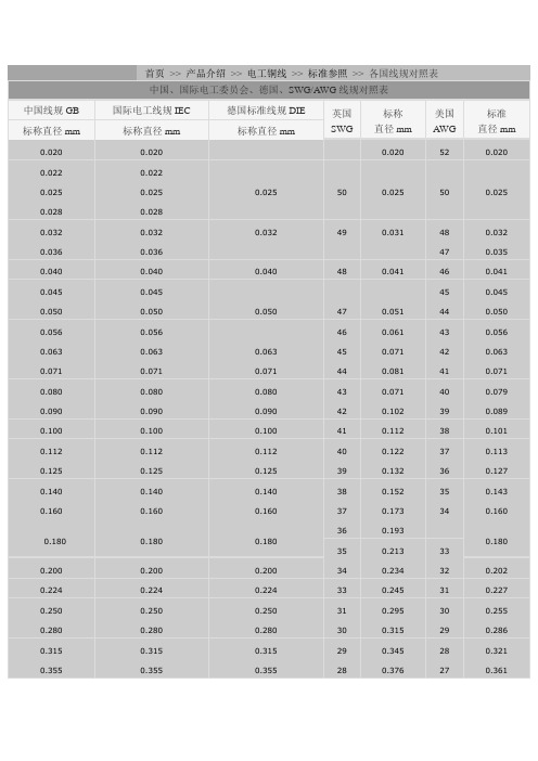
首页>> 产品介绍>> 电工铜线>> 标准参照>> 各国线规对照表中国、国际电工委员会、德国、SWG/AWG线规对照表中国线规GB 国际电工线规IEC 德国标准线规DIE 英国SWG标称直径mm美国AWG标准直径mm标称直径mm 标称直径mm 标称直径mm0.020 0.020 0.020 52 0.0200.022 0.0220.025 0.025 0.025 50 0.025 50 0.0250.028 0.0280.032 0.032 0.032 49 0.031 48 0.0320.036 0.036 47 0.0350.040 0.040 0.040 48 0.041 46 0.0410.045 0.045 45 0.0450.050 0.050 0.050 47 0.051 44 0.0500.056 0.056 46 0.061 43 0.0560.063 0.063 0.063 45 0.071 42 0.0630.071 0.071 0.071 44 0.081 41 0.0710.080 0.080 0.080 43 0.071 40 0.0790.090 0.090 0.090 42 0.102 39 0.0890.100 0.100 0.100 41 0.112 38 0.1010.112 0.112 0.112 40 0.122 37 0.1130.125 0.125 0.125 39 0.132 36 0.1270.140 0.140 0.140 38 0.152 35 0.1430.160 0.160 0.160 37 0.173 34 0.1600.180 0.180 0.180 36 0.1930.180 35 0.213 330.200 0.200 0.200 34 0.234 32 0.202 0.224 0.224 0.224 33 0.245 31 0.227 0.250 0.250 0.250 31 0.295 30 0.255 0.280 0.280 0.280 30 0.315 29 0.286 0.315 0.315 0.315 29 0.345 28 0.321 0.355 0.355 0.355 28 0.376 27 0.36136 0.127 0.0050 0.124 0.0049 0.130 0.0051 0.010 0.0004 0.147 0.0058 0.020 0.0008 0.160 0.006337 0.114 0.0045 0.112 0.0044 0.117 0.0046 0.008 0.0003 0.132 0.0052 0.020 0.0008 0.145 0.005738 0.102 0.0040 0.099 0.0039 0.104 0.0041 0.008 0.0003 0.119 0.0047 0.018 0.0007 0.130 0.005139 0.089 0.0035 0.086 0.0034 0.091 0.0036 0.005 0.0002 0.104 0.0041 0.015 0.0006 0.114 0.004540 0.079 0.0031 0.076 0.0030 0.081 0.0032 0.005 0.0002 0.094 0.0037 0.015 0.0006 0.102 0.004041 0.071 0.0028 0.069 0.0027 0.074 0.0029 0.005 0.0002 0.084 0.0033 0.013 0.0005 0.091 0.003642 0.064 0.0025 0.061 0.0024 0.066 0.0026 0.005 0.0002 0.076 0.0030 0.010 0.0004 0.081 0.003243 0.056 0.0022 0.053 0.0021 0.058 0.0023 0.003 0.0001 0.066 0.0026 0.010 0.0004 0.074 0.002944 0.051 0.0020 0.048 0.0019 0.053 0.0021 0.003 0.0001 0.061 0.0024 0.010 0.0004 0.069 0.002745 0.0447 0.00176 0.0025 0.00010 0.0521 0.00205 0.0076 0.0003 0.0584 0.002346 0.0399 0.00157 0.0025 0.00010 0.0470 0.00185 0.0076 0.0003 0.0533 0.002147 0.0356 0.00140 0.0025 0.00010 0.0432 0.00170 0.0076 0.0003 0.0483 0.001948 0.0315 0.00124 0.0025 0.00010 0.0381 0.00150 0.0051 0.0002 0.0432 0.001749 0.0282 0.00111 0.0025 0.00010 0.0330 0.00130 0.0051 0.0002 0.0381 0.001550 0.0251 0.00099 <0.0025 0.00010 0.0305 0.00120 0.0051 0.0002 0.0356 0.0014JIS(日本标准)-JIS:Class 0 (Zero) Enamelled WiresConductor Minimum Maximum MaximumDia. (mm) Toleranceof Dia.Thicknessof FilmOverallDia.Conductor Resistance20℃(Ω/km)±(mm) (mm) (mm)3.20 0.04 0.049 3.388 2.198 3.00 0.03 0.049 3.178 2.489 2.90 0.03 0.049 3.078 2.665 2.80 0.03 0.049 2.978 2.861 2.70 0.03 0.049 2.878 3.079 2.60 0.03 0.049 2.778 3.324 2.50 0.03 0.049 2.678 3.598 2.40 0.03 0.048 2.574 3.908 2.30 0.03 0.046 2.4684.260 2.20 0.03 0.046 2.368 4.662 2.10 0.03 0.045 2.2665.123 2.00 0.03 0.044 2.162 5.656 1.90 0.03 0.044 2.0626.278 1.80 0.03 0.042 1.9567.007 1.70 0.03 0.042 1.856 7.871 1.60 0.03 0.041 1.7548.906 1.50 0.03 0.041 1.654 10.16 1.40 0.03 0.039 1.548 11.70 1.30 0.03 0.039 1.448 13.61 1.20 0.03 0.037 1.342 16.04 1.10 0.03 0.037 1.242 19.17 1.00 0.03 0.036 1.138 23.33 0.95 0.02 0.034 1.072 25.38 0.90 0.02 0.033 1.020 28.35 0.85 0.02 0.032 0.966 31.87 0.80 0.02 0.031 0.914 36.08 0.75 0.02 0.030 0.860 41.19 0.70 0.02 0.028 0.804 47.47 0.65 0.02 0.027 0.752 55.31 0.60 0.02 0.026 0.698 65.260.55 0.02 0.025 0.646 78.15 0.50 0.01 0.025 0.586 91.43 0.45 0.01 0.024 0.532 114.2 0.40 0.01 0.023 0.480 145.3 0.37 0.01 0.022 0.446 170.6 0.35 0.01 0.021 0.424 191.2 0.32 0.01 0.021 0.394 230.0 0.30 0.01 0.021 0.374 262.9 0.29 0.01 0.020 0.360 285.7 0.28 0.010 0.020 0.350 307.3 0.27 0.010 0.020 0.340 331.4 0.26 0.010 0.020 0.330 358.4 0.25 0.008 0.020 0.318 382.5 0.24 0.008 0.020 0.308 416.2 0.23 0.008 0.020 0.298 454.5 0.22 0.008 0.019 0.286 498.4 0.21 0.008 0.019 0.276 549.0 0.20 0.008 0.019 0.266 607.6 0.19 0.008 0.019 0.256 676.2 0.18 0.008 0.019 0.246 757.2 0.17 0.008 0.018 0.232 853.5 0.16 0.008 0.018 0.222 969.5 0.15 0.008 0.017 0.210 1111 0.14 0.008 0.017 0.200 1286 0.13 0.008 0.017 0.190 1505 0.12 0.008 0.017 0.180 1786 0.11 0.008 0.016 0.166 2153 0.10 0.008 0.016 0.156 2647 0.09 0.006 0.015 0.143 3175 0.08 0.006 0.013 0.130 4091 0.07 0.006 0.012 0.118 54690.06 0.006 0.011 0.106 77610.05 0.004 0.010 0.094 107000.04 0.003 0.009 0.082 16530JIS(日本标准)- JIS:Class 1 Enamelled WiresConductor Minimum Maximum MaximumDia. (mm) Toleranceof Dia.±(mm)Thicknessof Film(mm)OverallDia.(mm)Conductor Resistance20℃(Ω/km)3.20 0.04 0.034 3.338 2.198 3.00 0.03 0.034 3.128 2.489 2.90 0.03 0.034 3.028 2.665 2.80 0.03 0.034 2.928 2.861 2.70 0.03 0.034 2.828 3.079 2.60 0.03 0.034 2.728 3.324 2.50 0.03 0.034 2.628 3.598 2.40 0.03 0.033 2.528 3.908 2.30 0.03 0.032 2.4224.260 2.20 0.03 0.032 2.322 4.662 2.10 0.03 0.031 2.2205.123 2.00 0.03 0.030 2.118 5.656 1.90 0.03 0.030 2.0186.278 1.80 0.03 0.029 1.9147.007 1.70 0.03 0.029 1.814 7.871 1.60 0.03 0.028 1.7128.906 1.50 0.03 0.028 1.612 10.16 1.40 0.03 0.027 1.508 11.70 1.30 0.03 0.027 1.408 13.61 1.20 0.03 0.026 1.304 16.04 1.10 0.03 0.026 1.204 19.171.00 0.03 0.025 1.102 23.33 0.95 0.02 0.024 1.038 25.38 0.90 0.02 0.023 0.986 28.35 0.85 0.02 0.022 0.934 31.87 0.80 0.02 0.021 0.882 36.08 0.75 0.02 0.020 0.830 41.19 0.70 0.02 0.019 0.776 47.47 0.65 0.02 0.018 0.724 55.31 0.60 0.02 0.017 0.672 65.26 0.55 0.02 0.017 0.620 78.15 0.50 0.01 0.017 0.560 91.43 0.45 0.01 0.016 0.508 114.2 0.40 0.01 0.015 0.456 145.3 0.37 0.01 0.014 0.424 170.6 0.35 0.01 0.014 0.402 191.2 0.32 0.01 0.014 0.372 230.0 0.30 0.01 0.014 0.352 262.9 0.29 0.01 0.013 0.340 285.7 0.28 0.01 0.013 0.330 307.3 0.27 0.010 0.013 0.320 331.4 0.26 0.010 0.013 0.310 358.4 0.25 0.008 0.013 0.298 382.5 0.24 0.008 0.013 0.288 416.2 0.23 0.008 0.013 0.278 454.5 0.22 0.008 0.012 0.266 498.4 0.21 0.008 0.012 0.256 549.0 0.20 0.008 0.012 0.246 607.6 0.19 0.008 0.012 0.236 676.2 0.18 0.008 0.012 0.226 757.2 0.17 0.008 0.011 0.214 853.5 0.16 0.008 0.011 0.204 969.50.15 0.008 0.010 0.192 11110.14 0.008 0.010 0.182 12860.13 0.008 0.010 0.172 15050.12 0.008 0.010 0.162 17860.11 0.008 0.009 0.150 21530.10 0.008 0.009 0.140 26470.09 0.006 0.008 0.128 31750.08 0.006 0.007 0.118 40910.07 0.006 0.006 0.106 54690.06 0.006 0.006 0.096 77610.05 0.004 0.005 0.083 107000.04 0.003 0.004 0.070 165300.03 0.003 0.004 0.058 31040 JIS(日本标准)- JIS:Class 2 Enamelled WiresConductor Minimum Maximum MaximumDia. (mm) Toleranceof Dia.±(mm)Thicknessof Film(mm)OverallDia.(mm)Conductor Resistance20℃(Ω/km)1.00 0.012 0.017 1.062 22.49 0.95 0.010 0.017 1.008 24.84 0.90 0.010 0.016 0.956 27.71 0.85 0.010 0.015 0.904 31.11 0.80 0.010 0.015 0.852 35.17 0.75 0.008 0.014 0.798 39.87 0.70 0.008 0.013 0.746 45.84 0.65 0.008 0.012 0.694 53.26 0.60 0.008 0.012 0.644 62.64 0.55 0.006 0.012 0.592 74.18 0.50 0.006 0.012 0.542 89.95 0.45 0.006 0.011 0.490 112.10.40 0.005 0.011 0.439 141.7 0.37 0.005 0.010 0.407 165.9 0.35 0.005 0.010 0.387 185.7 0.32 0.005 0.010 0.357 222.8 0.30 0.005 0.010 0.337 254.0 0.29 0.004 0.009 0.324 273.9 0.28 0.004 0.009 0.314 294.1 0.27 0.004 0.009 0.304 316.6 0.26 0.004 0.009 0.294 341.8 0.25 0.004 0.009 0.284 370.2 0.24 0.004 0.009 0.274 402.2 0.23 0.004 0.009 0.264 438.6 0.22 0.004 0.008 0.252 480.1 0.21 0.003 0.008 0.241 522.8 0.20 0.003 0.008 0.231 577.2 0.19 0.003 0.008 0.221 640.6 0.18 0.003 0.008 0.211 715.0 0.17 0.003 0.007 0.199 803.2 0.16 0.003 0.007 0.189 908.8 0.15 0.003 0.006 0.177 1037 0.14 0.003 0.006 0.167 1193 0.13 0.003 0.006 0.157 1389 0.12 0.003 0.006 0.147 1636 0.11 0.003 0.005 0.135 1957 0.10 0.003 0.005 0.125 2381 0.09 0.003 0.005 0.113 2959 0.08 0.003 0.005 0.103 3778 0.07 0.003 0.004 0.091 4990 0.06 0.003 0.004 0.081 6966 0.05 0.003 0.004 0.069 10240 0.04 0.002 0.003 0.056 156700.03 0.002 0.003 0.044 28870 0.025 0.002 0.003 0.037 42780JIS(日本标准)- JIS:Class 3 Enamelled WireConductor Minimum Maximum MaximumDia. (mm) Toleranceof Dia.±(mm)Thicknessof Film(mm)OverallDia.(mm)Conductor Resistance20℃(Ω/km)1.60 0.020 0.016 1.660 8.794 1.50 0.016 0.016 1.560 9.968 1.40 0.016 0.015 1.456 11.46 1.30 0.016 0.015 1.356 13.32 1.20 0.012 0.014 1.252 15.55 1.10 0.012 0.014 1.152 18.54 1.00 0.012 0.013 1.050 22.49 0.95 0.010 0.013 0.996 24.84 0.90 0.010 0.012 0.944 27.71 0.85 0.010 0.011 0.892 31.11 0.80 0.010 0.011 0.840 35.17 0.75 0.008 0.010 0.786 39.87 0.70 0.008 0.009 0.734 45.84 0.65 0.008 0.008 0.682 53.26 0.60 0.008 0.008 0.632 62.64 0.55 0.006 0.008 0.581 74.18 0.50 0.006 0.008 0.531 89.95 0.45 0.006 0.007 0.479 112.1 0.40 0.005 0.007 0.429 141.7 0.37 0.005 0.007 0.397 165.9 0.35 0.005 0.007 0.377 185.7 0.32 0.005 0.007 0.347 222.8 0.30 0.005 0.007 0.327 254.00.29 0.004 0.006 0.315 273.9 0.28 0.004 0.006 0.305 294.1 0.27 0.004 0.006 0.295 316.6 0.26 0.004 0.006 0.285 341.8 0.25 0.004 0.006 0.275 370.2 0.24 0.004 0.006 0.265 402.2 0.23 0.004 0.006 0.255 438.6 0.22 0.004 0.005 0.243 480.1 0.21 0.003 0.005 0.232 522.8 0.20 0.003 0.005 0.222 577.2 0.19 0.003 0.005 0.212 640.6 0.18 0.003 0.005 0.202 715.0 0.17 0.003 0.005 0.191 803.2 0.16 0.003 0.005 0.181 908.8 0.15 0.003 0.004 0.169 1037 0.14 0.003 0.004 0.159 1193 0.13 0.003 0.004 0.149 1389 0.12 0.003 0.004 0.139 1636 0.11 0.003 0.003 0.128 1957 0.10 0.003 0.003 0.118 2381 0.09 0.003 0.003 0.107 2959 0.08 0.003 0.003 0.097 3778 0.07 0.003 0.003 0.085 4990 0.06 0.003 0.003 0.075 6966 0.05 0.003 0.003 0.064 10240 0.04 0.002 0.002 0.052 15670 0.03 0.002 0.002 0.040 28870 0.025 0.002 0.002 0.034 42780BS(British Standard)Conductor Grade 1 Grade 2Nom (mm)Max(mm)Min(mm)MaxOverallDia.(mm)MinIncreasein Dia.(mm)MaxOverallDia.(mm)MinIncreasein Dia.(mm)3.150 3.182 3.118 3.233 0.045 3.276 0.084 3.000 3.030 2.970 3.083 0.045 3.126 0.084 2.800 2.828 2.772 2.880 0.043 2.922 0.081 2.650 2.677 2.623 2.730 0.043 2.772 0.081 2.500 2.525 2.475 2.578 0.042 2.618 0.079 2.360 2.384 2.336 2.438 0.042 2.478 0.079 2.240 2.262 2.218 2.316 0.041 2.355 0.077 2.120 2.141 2.099 2.196 0.041 2.235 0.077 2.000 2.020 1.980 2.074 0.040 2.112 0.075 1.900 1.919 1.881 1.974 0.040 2.012 0.075 1.800 1.818 1.782 0.872 0.039 1.909 0.073 1.700 1.717 1.683 1.772 0.039 1.809 0.073 1.600 1.616 1.584 1.670 0.038 1.706 0.071 1.500 1.515 1.485 1.570 0.038 1.606 0.071 1.400 1.414 1.386 1.468 0.036 1.502 0.069 1.320 1.333 1.307 1.388 0.036 1.422 0.069 1.250 1.263 1.237 1.316 0.035 1.349 0.067 1.180 1.192 1.168 1.246 0.035 1.279 0.067 1.120 1.131 1.109 1.184 0.034 1.217 0.065 1.060 1.071 1.049 1.124 0.034 1.157 0.065 1.000 1.010 0.990 1.062 0.034 1.094 0.063 0.950 0.960 0.940 1.012 0.034 1.044 0.063 0.900 0.909 0.891 0.959 0.032 0.989 0.060 0.850 0.859 0.841 0.909 0.032 0.939 0.060 0.800 0.808 0.792 0.855 0.030 0.884 0.056 0.750 0.758 0.742 0.805 0.030 0.834 0.056 0.710 0.717 0.703 0.762 0.028 0.789 0.0530.670 0.677 0.663 0.722 0.028 0.749 0.053 0.630 0.636 0.624 0.679 0.027 0.704 0.050 0.600 0.606 0.594 0.649 0.027 0.674 0.050 0.560 0.566 0.554 0.606 0.025 0.630 0.047 0.530 0.536 0.524 0.576 0.025 0.600 0.047 0.500 0.505 0.495 0.544 0.024 0.566 0.045 0.475 0.480 0.470 0.519 0.024 0.541 0.045 0.450 0.455 0.445 0.491 0.022 0.513 0.042 0.425 0.430 0.420 0.466 0.022 0.488 0.042 0.400 0.405 0.395 0.439 0.021 0.459 0.040 0.375 0.380 0.370 0.414 0.021 0.434 0.040 0.355 0.359 0.351 0.392 0.020 0.411 0.038 0.335 0.339 0.331 0.372 0.020 0.391 0.038 0.315 0.319 0.311 0.349 0.019 0.367 0.035 0.300 0.304 0.296 0.334 0.019 0.352 0.035 0.280 0.284 0.276 0.312 0.018 0.329 0.033 0.265 0.269 0.261 0.297 0.018 0.314 0.033 0.250 0.254 0.246 0.281 0.017 0.297 0.032 0.236 0.240 0.232 0.267 0.017 0.283 0.032 0.224 0.227 0.221 0.252 0.015 0.266 0.029 0.212 0.215 0.209 0.240 0.015 0.254 0.029 0.200 0.203 0.197 0.226 0.014 0.239 0.027 0.190 0.193 0.187 0.216 0.014 0.228 0.027 0.180 0.183 0.177 0.204 0.013 0.217 0.025 0.170 0.173 0.167 0.194 0.013 0.205 0.025 0.160 0.163 0.157 0.182 0.012 0.194 0.023 0.150 0.153 0.147 0.171 0.012 0.182 0.023 0.140 0.143 0.137 0.160 0.011 0.171 0.021 0.132 0.135 0.129 0.152 0.011 0.162 0.021 0.125 0.128 0.122 0.144 0.010 0.154 0.019 0.112 0.115 0.109 0.130 0.009 0.139 0.0170.100 0.103 0.097 0.117 0.008 0.125 0.016。
- 1、下载文档前请自行甄别文档内容的完整性,平台不提供额外的编辑、内容补充、找答案等附加服务。
- 2、"仅部分预览"的文档,不可在线预览部分如存在完整性等问题,可反馈申请退款(可完整预览的文档不适用该条件!)。
- 3、如文档侵犯您的权益,请联系客服反馈,我们会尽快为您处理(人工客服工作时间:9:00-18:30)。
触目惊心美国赌城房价暴跌75%,30万美元以9.5万的跳楼价转手美国内华达州拉斯维加斯北部的Coburn街区,这里的房屋没收率非常高译者:绎品翻译工作室(/ 欢迎交流英语学习方法,提供优质法律文件翻译服务,专业译员期待您的光临!)2011年9月16日美国拉斯维加斯(CNN)报道:冒着炙热的酷暑,居住在拉斯维加斯北部的迈克·弗瑞兹(Mike Forizs)出门倒垃圾。
“看看角落的那栋房子,窗户都破了。
”他说。
那俨然已经成了一些混混的聚会窝点,透过破碎的窗格,可以看到空酒瓶和苏打水瓶散落一地。
“准备离开此地的人们对这些已经无所谓了。
”欢迎来到美国房屋遭银行没收比率最高的地区之一,艳阳高照的拉斯维加斯!街道两边,随处可见“房屋出售”的牌子。
银行通知单散落在门前:“您的房子面临被拍卖的危险。
您的房屋贷款正在失去抵押赎回权。
这栋物业已经被认定为无主和放弃的物业。
”一些房屋内凡是值钱的东西,从管子到门把锁之类的,统统不见了。
到底是原来的屋主把这些东西带走了呢,还是遭人破坏了,不得而知。
这个小区的独栋房屋和车库是在2000年后兴建的,当时拉斯维加斯是美国发展最快的城市。
2000年至2010年期间,内华达州是发展最快的州。
这个区域还是一派崭新的面貌。
街道、人行道或车道上连一条裂缝也没有。
尽管这里的环境日渐荒凉,但是这些房屋的外观还是那么具有吸引力。
迈克·弗瑞兹以9.5万美元的价格买下位于拉斯维加斯的这栋房子;但原业主最初的买入价却超过30万美元但是拉斯维加斯遇到了经济衰退的严重打击。
内华达州房屋被银行没收的比率在全美高居榜首已经超过四年半时间;拉斯维加斯地区每4栋房屋中就有1栋正处于被银行没收的过程中。
房价暴跌了40%或更高。
对于像弗瑞兹这样的居民来说,每一天都面临着剧变和不稳定性。
“因为房子被银行没收,一些邻居已经搬走了。
这个小街区有三四栋房屋已经人去楼空了。
还有一些邻居正在想办法再贷款以保住自己的房屋。
” 弗瑞兹说。
当然,对于买家而言,这的确是入市的大好时机。
弗瑞兹就是其中的买家之一,几个月前他迁到这里。
他买的这栋错层式房屋最早的售价是30多万美元,但是弗瑞兹仅以9.5万美元就买下了。
“那家伙断供了,”他说起原业主,“银行也拿他没办法。
”拉斯维加斯的房屋没收率——8月份期间,118栋中有一栋遭银行没收——这是美国房地产过度繁荣的一个后遗症。
旅游业一直是拉斯维加斯的支柱产业,如今度假者和会议参加者在这里的开支都节约多了,或者压根儿就不来了。
居民们原来依靠小费就可以支付房款,如今却难以为继了。
失业率一直是两位数。
所有已售房屋中,约有四分之一是亏损出售的。
贷款人即原业主按揭欠款高于房屋的当前价值。
大拉斯维加斯房地产经纪人协会的公共关系负责人乔治·麦克凯布摇摇头。
麦克凯布毕生居于此地,他说:“2003年,我花了30万美元在Summerlin区买了一栋房子。
房地产繁荣期间,我一直居住在那里,那时我的邻居们常常围着门前的信箱聊天,‘我们都花了30万美元,我们将来可以卖到55万美元。
太不可思议了吧?喔!我们大家可是坐在金山上呀!’”另外,和多数美国人一样,这个小区中的许多人为买房贷了大笔的资金。
拉斯维加斯北部的一栋房屋,门上贴着的通知称房屋是空置的。
窗户已经破碎。
“而如今,”麦克凯布说,“他们在信箱边上谈论着谁谁谁的房屋可能或不可能被银行收走,或者谁谁谁准备断供。
”大拉斯维加斯房地产经纪人协会会长保罗·贝尔表示:“一些地区的房屋价值下跌了75%。
”现在,出现了一个新趋势:这里出售的房屋中一半以上采用现金交易。
这说明投机客和投资者已经冬眠,正在等待下一轮的房地产春天。
与此同时,业主们把房屋转售为租。
自2007年经济衰退开始以来,大拉斯维加斯房地产经纪人协会已经失去了超过6,000名会员。
Las Vegas (CNN) ‐‐ In the brutal heat, Mike Forizs ventures out of his North Las Vegas home to take out the trash."If I go over and look at the house on the corner, there are broken windows," he says. It appears to be a party hangout, with empty booze and soda bottles that can be seen through a broken pane."People don't care when they're getting ready to leave."Welcome to one of the top foreclosure areas in the nation, the sunny Las Vegas area. There are plenty of "For Sale" signs, up and down the street. Front doors are littered with tacked‐on notices: "You are in danger of losing your home. Your home loan is being foreclosed."This property has been determined to be vacant and abandoned."Some houses get stripped of whatever valuables are inside, from pipes to door hardware. It's impossible to know if the occupants took things with them, or if the empty houses fell to vandals.The neighborhood of single homes and garages was built in the early 2000s when Las Vegas was the fastest-growing metro area in the nation. Nevada was the fastest-growing state from 2000 to 2010.The area still looks new. There are no cracks in the streets, sidewalks or driveways, and the slow-growing desert landscape doesn't hurt the curb appeal.But the recession hit Vegas hard. Nevada's foreclosure rate has led the nation for more than four-and-a-half years; about 1-in-4 homes in the Vegas area is in some foreclosure process.Prices have dipped by 40% or more. It means turnover and uncertainty for residents such as Forizs."A couple of the neighbors have already moved out because of foreclosure. There's like three or four (other houses) just on this little block that are empty already. And there's a couple neighbors" trying to refinance, Forizs says.It does mean an upside for buyers, of course, including Forizs, who moved here a few months ago. His split-level home originally sold in themid-$300,000s. Forizs bought it for $95,000."Guy let it go," he says of the last owner. "The banks weren't working with him." Las Vegas' foreclosure rate -- one of every 118 housing units received a foreclosure filing August -- is a symptom of all the excesses of the American housing boom, but with shows, gambling and bright lights in easy reach.The downside of that tourism-driven economy: Vacationers andconvention-goers spend less or don't come at all. Residents who relied on tips to make the house payments found themselves unable to keep up. Unemployment is stuck in double digits.Of all the homes sold, about a quarter are short sales. The borrower owes more on the mortgage than the house is worth.George McCabe, a public relations executive who works with the Greater Las Vegas Association of Realtors, shakes his head. A lifelong resident, McCabe is contemplating his own neighborhood."I bought a home in 2003, in Summerlin, for $300,000," McCabe starts, speaking of a "master-planned," high-dollar suburban community."I lived in it through the boom, when my neighbors would gather around the mailbox and say, 'We all paid about three (hundred thousand dollars) and we can sell for 550 (thousand dollars). Isn't that amazing? Wow! We're all sitting on a gold mine.'"To boot, many of those neighbors, like many around the country, borrowed heavily on their equity."Now," McCabe says, "they stand around the mailbox talking about who may or may not be in danger of losing their homes to foreclosure or who's talking about walking away from their loan."Juggling the stats is Paul Bell, president of the Greater Las Vegas Association of Realtors."Some areas have declined as much as 75%" in home value, he says.Now, a new trend emerges: More than half the homes sold here are cash transactions. That's a sign that speculators and investors are waiting for the next boom. In the meantime, they turn the houses into rentals.The association lost more than 6,000 members since the start of the recession in 2007.。