MEMORY存储芯片PMP5201V,115中文规格书
MEMORY存储芯片THGBMNG5D1LBAIL中文规格书

[492]
FFU features
FFU_FEATURES
1
[491]
Operation codes timeout
OPERATION_CODES_TIMEOUT
1
[490:487] FFU Argument
FFU_ARG
4
[486]
Barrier support
BARRIER_SUPPORT
1
[485:309] Reserved
4
ORRECTLY_PROGRAMMED
[301:270] Vendor proprietary health report
VENDOR_PROPRIETARY 32
_HEALTH_REPORT
[269]
Device life time estimation type B
DEVICE_LIFE_TIME_EST_TYP_B
THGBMNG5D1LBAIL
Width Cell Type
2
R
4
R
2
R
8
R
8
R
8
R
12
R
4
R
1
R
1
R
1
R
1
R
2
R
12
R
3
R
3
R
3
R
3
R
3
R
5
R
5
R
5
R
1
R
2
R
3
R
4
R
1
R
4
R
1
R
1
R/W
1
R/W
1
MEMORY存储芯片MT41J256M16RE-15EIT中文规格书

10.Release frame sync generators from reset.Note that it is necessary to release the internal frame syncgenerators from reset,even if an external frame sync is being used,because the frame sync errordetection logic is built into the frame sync generator.(a)Take the respective frame sync generator(s)out of reset by setting the RFRST bit for the receiver,and/or the XFRST bit for the transmitter in GBLCTL.All other bits in GBLCTL should be left at theprevious state.(b)Read back from GBLCTL to ensure the bit(s)to which you wrote are successfully latched inGBLCTL before you proceed.11.Upon the first frame sync signal,McASP transfers begin.The McASP synchronizes to an edge on theframe sync pin,not the level on the frame sync pin.This makes it easy to release the state machineand frame sync generators from reset.(a)For example,if you configure the McASP for a rising edge transmit frame sync,then you do notneed to wait for a low level on the frame sync pin before releasing the McASP transmitter statemachine and frame sync generators from reset.23.0.21.1.3Separate Transmit and Receive InitializationIn many cases,it is desirable to separately initialize the McASP transmitter and receiver.For example,you may delay the initialization of the transmitter until the type of data coming in on the receiver is recognized.Or a change in the incoming data stream on the receiver may necessitate a reinitialization of thetransmitter.In this case,you may still follow the sequence outlined in Section23.0.21.1.2,but use it for each section (transmit,receive)individually.The GBLCTL register is aliased to RGBLCTL and XGBLCTL to facilitate separate initialization of transmit and receive sections.Also,make sure that the initialization or reinitialization sequence follows the guidelines in Bits WithRestrictions on When They May be Changed.23.0.21.1.4Importance of Reading Back GBLCTLIn Section23.0.21.1.2,steps4b,5b,7c,9b,and10b state that GBLCTL should be read back until the bits that were written are successfully latched.This is important,because the transmitter and receiver state machines run off of the respective bit clocks,which are typically about tens to hundreds of times slower than the DSP's internal bus clock.Therefore,it takes many cycles between when the DSP writes toGBLCTL(or RGBLCTL and XGBLCTL),and when the McASP actually recognizes the write operation.If you skip this step,then the McASP may never see the reset bits in the global control registers getasserted and deasserted;resulting in an uninitialized McASP.Therefore,the logic in McASP has been implemented such that once the DSP writes GBLCTL,RGBLCTL, or XGBLCTL,the resulting write is not visible by reading back GBLCTL until the McASP has recognized the change.This typically requires two bit clocks plus two DSP bus clocks to occur.Also,if the bit clocks can be completely stopped,any software that polls GBLCTL should be implemented with a time-out.If GBLCTL does not have a time-out,and the bit clock stops,the changes written toGBLCTL will not be reflected until the bit clock restarts.Finally,please note that while RGBLCTL and XGBLCTL allow separate changing of the receive andtransmit halves of GBLCTL,they also immediately reflect the updated value(useful for debug purposes).Only GBLCTL can be used for the read back step.23.0.21.1.5Synchronous Transmit and Receive Operation(ASYNC=0)When ASYNC=0in ACLKXCTL,the transmit and receive sections operate synchronously from thetransmit section clock and transmit frame sync signals(Figure23-15).The receive section may have a different(but compatible in terms of slot size)data format.Note that when ASYNC=0,XCLK isautomatically inverted to produce RCLK(note the inversion on the ASYNC multiplexer as shown inFigure23-16).Table23-3.Channel Status and User Data for Each DIT BlockFrame Subframe Preamble Channel Status defined in:User Data defined in: Defined by DITCSRA0,DITCSRB0,DITUDRA0,DITUDRB001(L)B DITCSRA0[0]DITUDRA0[0]02(R)W DITCSRB0[0]DITUDRB0[0]11(L)M DITCSRA0[1]DITUDRA0[1]12(R)W DITCSRB0[1]DITUDRB0[1]21(L)M DITCSRA0[2]DITUDRA0[2]22(R)W DITCSRB0[2]DITUDRB0[2]……………311(L)M DITCSRA0[31]DITUDRA0[31]312(R)W DITCSRB0[31]DITUDRB0[31] Defined by DITCSRA1,DITCSRB1,DITUDRA1,DITUDRB1321(L)M DITCSRA1[0]DITUDRA1[0]322(R)W DITCSRB1[0]DITUDRB1[0]……………631(L)M DITCSRA1[31]DITUDRA1[31]632(R)W DITCSRB1[31]DITUDRB1[31] Defined by DITCSRA2,DITCSRB2,DITUDRA2,DITUDRB2641(L)M DITCSRA2[0]DITUDRA2[0]642(R)W DITCSRB2[0]DITUDRB2[0]……………951(L)M DITCSRA2[31]DITUDRA2[31]952(R)W DITCSRB2[31]DITUDRB2[31] Defined by DITCSRA3,DITCSRB3,DITUDRA3,DITUDRB3961(L)M DITCSRA3[0]DITUDRA3[0]962(R)W DITCSRB3[0]DITUDRB3[0]……………1271(L)M DITCSRA3[31]DITUDRA3[31]1272(R)W DITCSRB3[31]DITUDRB3[31] Defined by DITCSRA4,DITCSRB4,DITUDRA4,DITUDRB41281(L)M DITCSRA4[0]DITUDRA4[0]1282(R)W DITCSRB4[0]DITUDRB4[0]……………1591(L)M DITCSRA4[31]DITUDRA4[31]1592(R)W DITCSRB4[31]DITUDRB4[31] Defined by DITCSRA5,DITCSRB5,DITDRA5,DITUDRB51601(L)M DITCSRA5[0]DITUDRA5[0]1602(R)W DITCSRB5[0]DITUDRB5[0]……………1911(L)M DITCSRA5[31]DITUDRA5[31]1912(R)W DITCSRB5[31]DITUDRB5[31]。
MEMORY存储芯片PTVS16VS1UR,115中文规格书

© Nexperia B.V. 2017. All rights reserved PTVSxS1UR_SER All information provided in this document is subject to legal disclaimers.Product data sheet Rev. 3 — 10 January 2011 10 of 12Nexperia PTVSxS1UR series 400 W Transient Voltage Suppressor13.Legal information13.1 Data sheet status[1]Please consult the most recently issued document before initiating or completing a design. [2]The term ‘short data sheet’ is explained in section “Definitions”. [3]The product status of device(s) described in this document may have changed since this document was published and may differ in case of multiple devices. The latest product status information is available on the Internet at URL .13.2 DefinitionsDraft — The document is a draft version only. The content is still underinternal review and subject to formal approval, which may result inmodifications or additions. Nexperia does not give anyrepresentations or warranties as to the accuracy or completeness ofinformation included herein and shall have no liability for the consequences ofuse of such information.Short data sheet — A short data sheet is an extract from a full data sheetwith the same product type number(s) and title. A short data sheet is intendedfor quick reference only and should not be relied upon to contain detailed andfull information. For detailed and full information see the relevant full datasheet, which is available on request via the local Nexperia salesoffice. In case of any inconsistency or conflict with the short data sheet, thefull data sheet shall prevail.Product specification — The information and data provided in a Productdata sheet shall define the specification of the product as agreed betweenNexperia and its customer, unless Nexperia andcustomer have explicitly agreed otherwise in writing. In no event however,shall an agreement be valid in which the Nexperia product isdeemed to offer functions and qualities beyond those described in theProduct data sheet.13.3 Disclaimers Limited warranty and liability — Information in this document is believed to be accurate and reliable. However, Nexperia does not give any representations or warranties, expressed or implied, as to the accuracy or completeness of such information and shall have no liability for the consequences of use of such information. In no event shall Nexperia be liable for any indirect, incidental, punitive, special or consequential damages (including - without limitation - lost profits, lost savings, business interruption, costs related to the removal or replacement of any products or rework charges) whether or not such damages are based on tort (including negligence), warranty, breach of contract or any other legal theory. Notwithstanding any damages that customer might incur for any reason whatsoever, Nexperia’s aggregate and cumulative liability towards customer for the products described herein shall be limited in accordance with the Terms and conditions of commercial sale of Nexperia.Right to make changes — Nexperia reserves the right to make changes to information published in this document, including without limitation specifications and product descriptions, at any time and without notice. This document supersedes and replaces all information supplied prior to the publication hereof.Suitability for use — Nexperia products are not designed, authorized or warranted to be suitable for use in life support, life-critical or safety-critical systems or equipment, nor in applications where failure or malfunction of a Nexperia product can reasonably be expected to result in personal injury, death or severe property or environmental damage. Nexperia accepts no liability for inclusion and/or use of Nexperia products in such equipment or applications and therefore such inclusion and/or use is at the customer’s own risk.Applications — Applications that are described herein for any of these products are for illustrative purposes only. Nexperia makes no representation or warranty that such applications will be suitable for the specified use without further testing or modification. Customers are responsible for the design and operation of their applications and products using Nexperia products, and Nexperia accepts no liability for any assistance with applications or customer product design. It is customer’s sole responsibility to determine whether the Nexperia product is suitable and fit for the customer’s applications and products planned, as well as for the planned application and use of customer’s third party customer(s). Customers should provide appropriate design and operating safeguards to minimize the risks associated with their applications and products. Nexperia does not accept any liability related to any default, damage, costs or problem which is based on any weakness or default in the customer’s applications or products, or the application or use by customer’s third party customer(s). Customer is responsible for doing all necessarytesting for the customer’s applications and products using Nexperiaproducts in order to avoid a default of the applications andthe products or of the application or use by customer’s third partycustomer(s). Nexperia does not accept any liability in this respect.Limiting values — Stress above one or more limiting values (as defined inthe Absolute Maximum Ratings System of IEC 60134) will cause permanentdamage to the device. Limiting values are stress ratings only and (proper)operation of the device at these or any other conditions above those given inthe Recommended operating conditions section (if present) or theCharacteristics sections of this document is not warranted. Constant orrepeated exposure to limiting values will permanently and irreversibly affectthe quality and reliability of the device.Terms and conditions of commercial sale — Nexperiaproducts are sold subject to the general terms and conditions of commercialsale, as published at /profile/terms , unless otherwiseagreed in a valid written individual agreement. In case an individualagreement is concluded only the terms and conditions of the respectiveagreement shall apply. Nexperia hereby expressly objects toapplying the customer’s general terms and conditions with regard to thepurchase of Nexperia products by customer.No offer to sell or license — Nothing in this document may be interpreted orconstrued as an offer to sell products that is open for acceptance or the grant,conveyance or implication of any license under any copyrights, patents orother industrial or intellectual property rights.Export control — This document as well as the item(s) described hereinmay be subject to export control regulations. Export might require a priorauthorization from national authorities.Document status [1][2]Product status [3]Definition Objective [short] data sheetDevelopment This document contains data from the objective specification for product development. Preliminary [short] data sheetQualification This document contains data from the preliminary specification. Product [short] data sheetProduction This document contains the product specification.© Nexperia B.V. 2017. All rights reserved PTVSxS1UR_SER All information provided in this document is subject to legal disclaimers.Product data sheet Rev. 3 — 10 January 2011 4 of 12Nexperia PTVSxS1UR series 400 W Transient Voltage Suppressor6.Thermal characteristics[1]Device mounted on an FR4Printed-Circuit Board (PCB), single-sided copper, tin-plated and standard footprint.[2]Device mounted on an FR4PCB, single-sided copper, tin-plated, mounting pad for cathode 1cm 2.[3]Device mounted on a ceramic PCB, Al 2O 3, standard footprint.[4]Soldering point of cathode tab.7.CharacteristicsTable 8.Thermal characteristics Symbol Parameter Conditions Min Typ Max Unit R th(j-a)thermal resistance fromjunction to ambient in free air [1]--220K/W [2]--130K/W [3]--70K/W R th(j-sp)thermal resistance from junction to solder point [4]--18K/W Table 9.Characteristics per type; PTVS3V3S1UR to PTVS7V0S1URT j =25°C unless otherwise specified.Type number Reverse standoffvoltageV RWM (V)Breakdown voltage V BR (V)Reverse leakage current I RM (μA)Clamping voltage V CL (V)I R =10mAat V RWM (V)MaxMin Typ Max Typ Max Max I PPM (A)PTVS3V3S1UR3.3 5.20 5.60 6.0056008.043.8PTVS5V0S1UR5.06.40 6.707.0054009.243.5PTVS6V0S1UR6.0 6.677.027.37540010.338.8PTVS6V5S1UR6.57.227.607.98525011.235.7PTVS7V0S1UR 7.07.788.208.60310012.033.3Table 10.Characteristics per type; PTVS7V5S1UR to PTVS64VS1URT j =25°C unless otherwise specified.Type number Reverse standoffvoltageV RWM (V)Breakdown voltage V BR (V)Reverse leakage current I RM (μA)Clamping voltage V CL (V)I R =1mAat V RWM (V)MaxMin Typ Max Typ Max Max I PPM (A)PTVS7V5S1UR7.58.338.779.210.25012.931.0PTVS8V0S1UR8.08.899.369.830.032513.629.4PTVS8V5S1UR8.59.449.9210.400.011014.427.8PTVS9V0S1UR9.010.0010.5511.100.005515.426.0PTVS10VS1UR1011.1011.7012.300.005 2.517.023.5PTVS11VS1UR1112.2012.8513.500.005 2.518.222.0PTVS12VS1UR1213.3014.0014.700.005 2.519.920.1PTVS13VS1UR1314.4015.1515.900.0010.121.518.6。
MEMORY存储芯片MT41J512M8RA-15EAIT中文规格书

Notes: 1.Maximum limit not applicable.2.Micron tDLLK values support the legacy JEDEC tDLLK specifications.3.DDR4-1600 AC timing parameters apply if DRAM operates at lower than 1600 MT/s datarate.4.Data rate is greater than or equal to 1066 Mb/s.5.WRITE-to-READ when CRC and DM are both not enabled.6.WRITE-to-READ delay when CRC and DM are both enabled.7.The start of internal write transactions is defined as follows:•For BL8 (fixed by MRS and on-the-fly): rising clock edge four clock cycles after WL•For BC4 (on-the-fly): rising clock edge four clock cycles after WL•For BC4 (fixed by MRS): rising clock edge two clock cycles after WL8.For these parameters, the device supports t n PARAM [n CK] = ROUND{t PARAM [ns]/t CK(AVG) [ns]} according to the rounding algorithms found in the Converting Time-BasedSpecifications to Clock-Based Requirements section, in clock cycles, assuming all inputclock jitter specifications are satisfied.9.When operating in 1t CK WRITE preamble mode.10.When operating in 2t CK WRITE preamble mode.11.When CA parity mode is selected and the DLLoff mode is used, each REF command re-quires an additional "PL" added to t RFC refresh time.12.DRAM devices should be evenly addressed when being accessed. Disproportionate ac-cesses to a particular row address may result in reduction of the product lifetime and/orreduction in data retention ability.13.Applicable from t CK (AVG) MIN to t CK (AVG) MAX as stated in the Speed Bin tables.14.JEDEC specifies a minimum of five clocks.15.The maximum read postamble is bound by t DQSCK (MIN) plus t QSH (MIN) on the leftside and t HZ(DQS) MAX on the right side.16.The reference level of DQ output signal is specified with a midpoint as a widest part ofoutput signal eye, which should be approximately 0.7 × V DDQ as a center level of thestatic single-ended output peak-to-peak swing with a driver impedance of 34 ohms andan effective test load of 50 ohms to V TT = V DDQ.17.JEDEC hasn't agreed upon the definition of the deterministic jitter; the user should fo-cus on meeting the total limit.18.Spread spectrum is not included in the jitter specification values. However, the inputclock can accommodate spread-spectrum at a sweep rate in the range of 20–60 kHz withan additional 1% of t CK (AVG) as a long-term jitter component; however, the spreadspectrum may not use a clock rate below t CK (AVG) MIN.19.The actual t CAL minimum is the larger of 3 clocks or 3.748ns/t CK; the table lists the ap-plicable clocks required at targeted speed bin.20.The maximum READ preamble is bounded by t LZ(DQS) MIN on the left side and t DQSCK(MAX) on the right side. See figure in the Clock to Data Strobe Relationship section.Boundary of DQS Low-Z occurs one cycle earlier in 2t CK toggle mode, as illustrated inthe READ Preamble section.21.DQ falling signal middle-point of transferring from HIGH to LOW to first rising edge ofDQS differential signal cross-point.22.The t PDA_S/t PDA_H parameters may use the t DS/t DH limits, respectively, if the signal isLOW the entire BL8.Converting Time-Based Specifications to Clock-Based RequirementsSoftware algorithms for calculation of timing parameters are subject to potential round-ing errors when converting DRAM timing requirements to system clocks; for example, amemory clock with a nominal frequency of 933.33...3 MHz which yields a clock period of 1.0714********...ns. It is unrealistic to represent all digits after the decimal point ex-actly and some sort of rounding needs to be done.DDR4 SDRAM SPD-based specifications use a minimum granularity for SPD-associated timing parameters of 1ps. Clock periods such as t CK (AVG) MIN are defined to the near-est picosecond. For example, 1.0714********...ns is stated as 1071ps. Parameters such as t AA MIN are specified in units of time (nanoseconds) and require mathematical com-putation to convert to system clocks (n CK). Rules for rounding allow optimization of device performance without violating device parameters. These SPD algorithms rely on results that are within n CK adjustment factors on device testing and specification to avoid losing performance due to rounding errors when using SPD-based parameters. Note that JEDEC also defines an n CK adjustment factor, but mandates the inverse n CK adjustment factor be used in case of conflicting results, so only the inverse n CK adjust-ment factor is discussed here.Guidance converting SPD associated timing parameters to system clock requirements:•Round the application clock period up to the nearest picosecond.•Express the timing specification and application clock period in picoseconds; scaling a nanosecond-based parameter value by 1000 allows programmers to use integer math instead of real math by expressing timing in ps.•Divide the picosecond-based parameter by the picoseconds based application clock period.•Add an inverse n CK adjustment factor of 97.4%.•Truncate down to the next lower integer value.•n CK = Truncate[(parameter in ps)/(application t CK in ps) + (974/1000)].Guidance converting nonSPD associated timing parameters to system clock require-ments:•Divide the time base specification (in ns) and divided by the clock period (in ns).•The resultant is set to the next higher integer number of clocks.•n CK = Ceiling[(parameter in ns/application t CK in ns)].。
MEMORY存储芯片MAX125CEAX+D中文规格书
General DescriptionThe MAX125/MAX126 are high-speed, multichannel,14-bit data-acquisition systems (DAS) with simultaneous track/holds (T/Hs). These devices contain a 14-bit, 3µs,successive-approximation analog-to-digital converter (ADC), a +2.5V reference, a buffered reference input,and a bank of four simultaneous-sampling T/H ampli-fiers that preserve the relative phase information of the sampled inputs. The MAX125/MAX126 have two multi-plexed inputs for each T/H, allowing a total of eight inputs. In addition, the converter is overvoltage tolerant to ±17V; a fault condition on any channel will not harm the I C. Available input ranges are ±5V (MAX125) and ±2.5V (MAX126).An on-board sequencer converts one to four channels per CONVST pulse. In the default mode, one T/H output (CH1A) is converted. An interrupt signal (INT ) is provided after the last conversion is complete. Convert two,three, or four channels by reprogramming the MAX125/MAX126 through the bidirectional parallel interface. Once programmed, the MAX125/MAX126continue to convert the specified number of channels per CONVST pulse until they are reprogrammed. The channels are converted sequentially, beginning with CH1. The INT signal always follows the end of the last conversion in a conversion sequence. The ADC con-verts each assigned channel in 3µs and stores the result in an internal 14x4 RAM. Upon completion of the conversions, data can be accessed by applying suc-cessive pulses to the RD pin. Four successive reads access four data words sequentially.The parallel interface’s data-access and bus-release timing specifications are compatible with most popular digital signal processors and 16-bit/32-bit microproces-sors, so the MAX125/MAX126 conversion results can be accessed without resorting to wait states.ApplicationsMultiphase Motor Control Power-Grid Synchronization Power-Factor Monitoring Digital Signal Processing Vibration and Waveform AnalysisFeatures♦Four Simultaneous-Sampling T/H Amplifiers with Two Multiplexed Inputs (eight single-ended inputs total)♦3µs Conversion Time per Channel ♦Throughput: 250ksps (1 channel)142ksps (2 channels)100ksps (3 channels)76ksps (4 channels)♦Input Range: ±5V (MAX125)±2.5V (MAX126)♦Fault-Protected Input Multiplexer (±17V)♦±5V Supplies♦Internal +2.5V or External Reference Operation ♦Programmable On-Board Sequencer ♦High-Speed Parallel DSP InterfaceMAX125/MAX126________________________________________________________________Ordering InformationTypical Operating Circuit appears at end of data sheet.Pin Configuration appears at end of data sheet.PART TEMP RANGE PIN-PACKAGEINL(LSB) MAX125CCAX 0°C to +70°C 36 SSOP ±4 MAX125CEAX -40°C to +85°C 36 SSOP ±4 MAX126CCAX 0°C to +70°C 36 SSOP ±4 MAX126CEAX-40°C to +85°C36 SSOP±4_______________Detailed DescriptionThe MAX125/MAX126 use a successive-approximation conversion technique and four simultaneous-sampling track/hold (T/H) amplifiers to convert analog signals into 14-bit digital outputs. Each T/H has two multiplexed inputs, allowing a total of eight inputs. Each T/H output is converted and stored in memory to be accessed sequentially by the parallel interface with successive read cycles. The MAX125/MAX126 internal micro-sequencer can be programmed to digitize one, two,three, or four inputs sampled simultaneously from either of the two banks of four inputs (see Figure 2).The conversion timing and control sequences are derived from a 16MH z external clock, the CONVSTM A X 125/M A X 1262x4-Channel, Simultaneous-Sampling 14-Bit DAS______________________________________________________________Pin DescriptionMAX125/MAX12614-Bit DAS_______________________________________________________________________________________Figure 2.Functional Diagram1ppm/°C (max) temperature drift. Connect an external reference at REFIN as shown in Figure 7. The minimum impedance is 7kΩfor DC currents in both normal oper-ation and shutdown. Bypass REFOUT with a 4.7µF low-ESR capacitor.Power-On Reset When power is first applied, the internal power-on-reset circuitry activates the MAX125/MAX126 with INT= high, ready to convert. The default conversion mode is Input Mux A/Single-Channel Conversion. See the Programming Modes section if other configurations are desired.After the power supplies have been stabilized, the reset time is 5µs; no conversions should be performed during this phase. At power-up, data in memory is undefined.Software Power-Down Software power-down is activated by setting bit A3 of the control word high (Table 1). It is asserted after the WR or CS rising edge, at which point the ADC immedi-ately powers down to a low quiescent-current state. AV DD drops to less than 1.5mA, and AV SS is reduced to less than 1mA. The ADC blocks and reference buffer are turned off, but the digital interface and the refer-ence remain active for fast power-up recovery. Wake up the MAX125/MAX126 by writing a control word (A0–A3, Table 1). The bidirectional interface interprets a logic zero at A3 as the start signal and powers up in the mode selected by A0, A1, and A2. The referencebuffer’s settling time and the bypass capacitor’s value dominate the power-up delay. With the recommended 4.7µF at REFOUT, the power-up delay is typically 5µs.Transfer Function The MAX125/MAX126 have bipolar input ranges. Fig-ure 8 shows the bipolar/output transfer function. Code transitions occur at successive-integer least significant bit (LSB) values. Output coding is twos-complement binary with 1LSB = 610µV for the MAX125 and 1LSB = 305µV for the MAX126.Output Demultiplexer An output demultiplexer circuit is useful for isolating data from one channel in a four-channel conversion sequence. Figure 9’s circuit uses the external 16MH z clock and the INT signal to generate four RD pulses and a latch clock to save data from the desired chan-nel. CS must be low during the four RD pulses. The channel is selected with the binary coding of two switches. A 16-bit 16373 latch simplifies layout.Motor-Control Applications Vector motor control requires monitoring of the individ-ual phase currents. In their most basic application, the MAX125/MAX126 simultaneously sample two currents (CH1A and CH2A, Figure 10) and preserve the neces-sary relative phase information. Only two of the three phase currents have to be digitized, because the third component can be mathematically derived with a coor-dinate transformation.MAX125/MAX12614-Bit DAS______________________________________________________________________________________ Figure 7.External Reference Figure 8. Bipolar Transfer FunctionMAX125/MAX1262x4-Channel, Simultaneous-Sampling14-Bit DASRevision History。
MEMORY存储芯片MT41K512M8RH-125IT E中文规格书
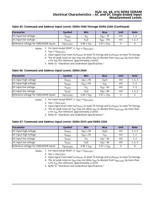
Table 85: Command and Address Input Levels: DDR4-1600 Through DDR4-2400 (Continued)Notes: 1.For input except RESET_n. V REF = V REFCA(DC).2.V REF = V REFCA(DC).3.Input signal must meet V IL /V IH(AC) to meet t IS timings and V IL /V IH(DC) to meet t IH timings.4.The AC peak noise on V REF may not allow V REF to deviate from V REFCA(DC) by more than±1% V DD (for reference: approximately ±12mV).5.Refer to “Overshoot and Undershoot Specifications.”Table 86: Command and Address Input Levels: DDR4-2666Notes: 1.For input except RESET_n. V REF = V REFCA(DC).2.V REF = V REFCA(DC).3.Input signal must meet V IL /V IH(AC) to meet t IS timings and V IL /V IH(DC) to meet t IH timings.4.The AC peak noise on V REF may not allow V REF to deviate from V REFCA(DC) by more than±1% V DD (for reference: approximately ±12mV).5.Refer to “Overshoot and Undershoot Specifications.”Table 87: Command and Address Input Levels: DDR4-2933 and DDR4-3200Notes: 1.For input except RESET_n. V REF = V REFCA(DC).2.V REF = V REFCA(DC).3.Input signal must meet V IL /V IH(AC) to meet t IS timings and V IL /V IH(DC) to meet t IH timings.4.The AC peak noise on V REF may not allow V REF to deviate from V REFCA(DC) by more than±1% V DD (for reference: approximately ±12mV).5.Refer to “Overshoot and Undershoot Specifications.”8Gb: x4, x8, x16 DDR4 SDRAM Electrical Characteristics – AC and DC Single-Ended Input Measurement LevelsFigure 223: Differential Input Slew Rate Definition for CK_t, CK_cV IH,diff,min V IL,diff,max0C K D i f f e r e n t i a l I n p u t V o l t a g e TR CK Differential Input Cross Point VoltageTo guarantee tight setup and hold times as well as output skew parameters with respectto clock and strobe, each cross point voltage of differential input signal CK_t, CK_c mustmeet the requirements shown below. The differential input cross point voltage V IX(CK) ismeasured from the actual cross point of true and complement signals to the midlevelbetween V DD and V SS .Figure 224: V IX(CK)DefinitionCK_tV SSV DD /2CK_cV DD8Gb: x4, x8, x16 DDR4 SDRAM Electrical Characteristics – AC and DC Differential Input Meas-urement LevelsData, Strobe, and Mask Overshoot and Undershoot SpecificationsTable 113: Data, Strobe, and Mask Overshoot and Undershoot/ SpecificationsFigure 231: Data, Strobe, and Mask Overshoot and Undershoot DefinitionDDQ absolute MAX SSQ absolute MIN DDQ absolute MAXSSQ MIN and V o l t s (V )V DDQ V SSQ Electrical Characteristics – AC and DC Output Measurement Levels Single-Ended OutputsTable 114: Single-Ended Output Levels8Gb: x4, x8, x16 DDR4 SDRAM Electrical Characteristics – AC and DC Output Measurement Levels。
MEMORY存储芯片MAX202ECPE中文规格书
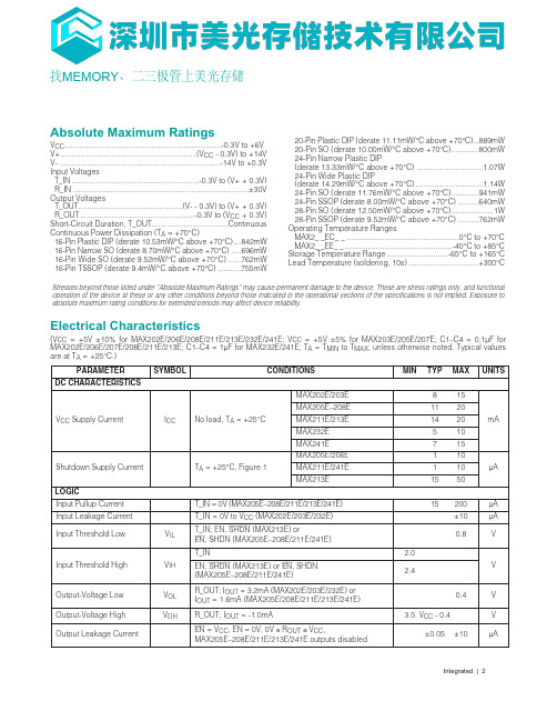
Integrated | 2Absolute Maximum RatingsV CC ..........................................................................-0.3V to +6VV+................................................................(V CC - 0.3V) to +14VV-............................................................................-14V to +0.3VInput VoltagesT_IN............................................................-0.3V to (V+ + 0.3V)R_IN...................................................................................±30VOutput VoltagesT_OUT.................................................(V- - 0.3V) to (V+ + 0.3V)R_OUT......................................................-0.3V to (V CC + 0.3V)Short-Circuit Duration, T_OUT....................................ContinuousContinuous Power Dissipation (T A = +70°C)16-Pin Plastic DIP (derate 10.53mW/°C above +70°C)....842mW16-Pin Narrow SO (derate 8.70mW/°C above +70°C).....696mW16-Pin Wide SO (derate 9.52mW/°C above +70°C)......762mW16-Pin TSSOP (derate 9.4mW/°C above +70°C)...........755mW 20-Pin Plastic DIP (derate 11.11mW/°C above +70°C)...889mW 20-Pin SO (derate 10.00mW/°C above +70°C).............800mW 24-Pin Narrow Plastic DIP (derate 13.33mW/°C above +70°C) ...............................1.07W 24-Pin Wide Plastic DIP (derate 14.29mW/°C above +70°C)................................1.14W 24-Pin SO (derate 11.76mW/°C above +70°C).............941mW 24-Pin SSOP (derate 8.00mW/°C above +70°C)..........640mW 28-Pin SO (derate 12.50mW/°C above +70°C)....................1W 28-Pin SSOP (derate 9.52mW/°C above +70°C)..........762mW Operating Temperature Ranges MAX2_ _EC_ _.....................................................0°C to +70°C MAX2_ _EE_ _...................................................-40°C to +85°C Storage Temperature Range.............................-65°C to +165°C Lead Temperature (soldering, 10s).................................+300°C Electrical Characteristics(V CC = +5V ±10% for MAX202E/206E/208E/211E/213E/232E/241E; V CC = +5V ±5% for MAX203E/205E/207E; C1–C4 = 0.1µF for MAX202E/206E/207E/208E/211E/213E; C1–C4 = 1µF for MAX232E/241E; T A = T MIN to T MAX ; unless otherwise noted. Typical values are at T A = +25°C.)Stresses beyond those listed under “Absolute Maximum Ratings” may cause permanent damage to the device. These are stress ratings only, and functional operation of the device at these or any other conditions beyond those indicated in the operational sections of the specifications is not implied. Exposure to absolute maximum rating conditions for extended periods may affect device reliability.找MEMORY 、二三极管上美光存储Integrated | 12MAX202E–MAX213E,MAX232E/MAX241E±15kV ESD-Protected, 5V RS-232 Transceivers Model. F igure 7b shows the current waveform for the 8kV IEC1000-4-2 level-four ESD contact-discharge test.The air-gap test involves approaching the device with a charged probe. The contact-discharge method con-nects the probe to the device before the probe is ener-gized.Machine Model The Machine Model for ESD tests all pins using a 200pF storage capacitor and zero discharge resis-tance. Its objective is to emulate the stress caused by contact that occurs with handling and assembly during manufacturing. Of course, all pins require this protec-tion during manufacturing, not just RS-232 inputs andFigure 7a. IEC1000-4-2 ESD Test Modelest, which is then discharged into the test device through a 1.5k Ω resistor.IEC1000-4-2The IEC1000-4-2 standard covers ESD testing and per-formance of finished equipment; it does not specifically refer to integrated circuits. The MAX202E/MAX203E–MAX213E, MAX232E/MAX241E help you design equipment that meets level 4 (the high-est level) of IEC1000-4-2, without the need for addition-al ESD-protection components.The major difference between tests done using the Human Body Model and IEC1000-4-2 is higher peak current in IEC1000-4-2, because series resistance is lower in the IEC1000-4-2 model. Hence, the ESD with-stand voltage measured to IEC1000-4-2 is generallylower than that measured using the Human BodyFigure 7b. IEC1000-4-2 ESD Generator Current Waveform Figure 6a. Human Body ESD Test ModelFigure 6b. Human Body Model Current Waveform。
MEMORY存储芯片MT41J256M16RE-15E中文规格书
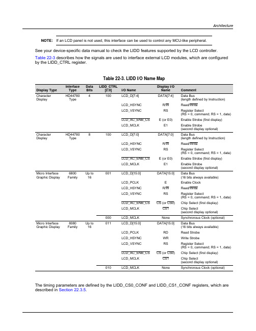
Architecture NOTE:If an LCD panel is not used,this interface can be used to control any MCU-like peripheral.See your device-specific data manual to check the LIDD features supported by the LCD controller.Table22-3describes how the signals are used to interface external LCD modules,which are configured by the LIDD_CTRL register.Table22-3.LIDD I/O Name MapDisplay Type InterfaceTypeDataBitsLIDD_CTRL[2:0]I/O NameDisplay I/OName CommentCharacter Display HD44780Type4100LCD_D[7:4]DATA[7:4]Data Bus(length defined by Instruction)LCD_HSYNC R/W Read/WriteLCD_VSYNC RS Register Select(RS=0,command;RS=1,data)LCD_AC_ENB_CS E(or E0)Enable Strobe(first display)LCD_MCLK E1Enable Strobe(second display optional)Character Display HD44780Type8100LCD_D[7:0]DATA[7:0]Data Bus(length defined by Instruction)LCD_HSYNC R/W Read/WriteLCD_VSYNC RS Register Select(RS=0,command;RS=1,data)LCD_AC_ENB_CS E(or E0)Enable Strobe(first display)LCD_MCLK E1Enable Strobe(second display optional)Micro Interface Graphic Display6800FamilyUp to16001LCD_D[15:0]DATA[15:0]Data Bus(16bits always available)LCD_PCLK E Enable ClockLCD_HSYNC R/W Read/WriteLCD_VSYNC RS Register Select(RS=0,command;RS=1,data)LCD_AC_ENB_CS CS(or CS0)Chip Select(first display)LCD_MCLK CS1Chip Select(second display optional)000LCD_MCLK None Synchronous Clock(optional)Micro Interface Graphic Display8080FamilyUp to16011LCD_D[15:0]DATA[15:0]Data Bus(16bits always available)LCD_PCLK RD Read StrobeLCD_HSYNC WR Write StrobeLCD_VSYNC RS Register Select(RS=0,command;RS=1,data)LCD_AC_ENB_CS CS(or CS0)Chip Select(first display)LCD_MCLK CS1Chip Select(second display optional)010LCD_MCLK None Synchronous Clock(optional)The timing parameters are defined by the LIDD_CS0_CONF and LIDD_CS1_CONF registers,which are described in Section22.3.5.Architecture Table22-7.Color/Grayscale Intensities and Modulation RatesDither Value(4-Bit Value from Palette)Intensity(0%is White)Modulation Rate(Ratio of ON to ON+OFF Pixels)00000.0%0000111.1%1/9001020.0%1/5001126.7%4/15010033.3%3/9010140.0%2/5011044.4%4/9011150.0%1/2100055.6%5/9100160.0%3/5101066.6%6/9101173.3%11/15110080.0%4/5110188.9%8/91110100.0%11111100.0%122.2.5.4.3Summary of Color DepthTable22-8.Number of Colors/Shades of Gray Available on ScreenNumber ofBPPPassive Mode(TFT_STN=0)Active Mode(TFT_STN=1) Monochrome(MONO_COLOR=1)Color(MONO_COLOR=0)Color Only(MONO_COLOR=0)12palette entries to select within 15grayscales 2palette entries to select within3375possible colors2palette entries to select within4096possible colors24palette entries to select within 15grayscales 4palette entries to select within3375possible colors4palette entries to select within4096possible colors416palette entries to select within 15grayscales 16palette entries to select within3375possible colors16palette entries to select within4096possible colors8Not relevant since it would consist in 256palette entries to select within15grayscales,but exists anyway 256palette entries to select3375possible colors256palette entries to select within4096possible colors12x3375possible colors4096possible colors16x3375possible colors(STN_565=1)Up to65536possible colors。