IBM25CPC710DF3B133中文资料
IBM小型机配件
X3755 CPU 内存板 42D3093 44R5988 42D3097 40K7532 42D3108 P6 550 CPU 内存板
42R6609 44V3841 模块 44V6625 97P5095
IBM P570 7782 cpu 内存板 实物拍摄
? IBM X366 X260 X3800 CPU 板
42D3097
X365 散热片 FRU: 90P5046
3850M2 散热片
? COMPAQ PL3000 风扇 PL5000 风扇 Nhomakorabea
3650T 风扇 扇组
风
X340 风扇 X342 风扇 00N7248 20L1399 5000 风 扇
59P2572 风扇 X255 风扇
06p3609 百兆网卡
13N2195 6I 阵列卡
59p2952 X360 远程卡
39R8852 sas 卡 IBM 服务器 X250 X350 7600 CPU 终结板 10L6936 73p9246 IBM 远程控制卡
09N7292 IBM 光纤网卡
?
IBM P550 5264 CPU 内存板
07P6825
07P6793 46K8035 P6 550 CPU 内存板
42D3107 IBM X3755 CPU 内存板
P550 IBM 5264 CPU 内存板 1.5G 2-WAY
P6 570 CPU 内存板
46K6860 42R5983 42R5967 散热片
海尔电脑X105终端培训资料

话术:这个本子虽然小,但是音响效果绝对不亚于14寸的本子音响。部分本子在播放高音时会 出现声音失真的情况,但是您听x105的音响效果,播放《青藏高原》都没有问题。主要是这个 音响设计很独特,它可以和桌面形成共振效果,把本子和桌面之间的空间当作共振箱体,从而 让您听到高保真的音质!
万小时以上。,而且用LED屏小本更能显得小巧轻薄
7
130万摄像头
内置摄像头节省了外部空间,无需携带,更方便了使用者在外 出旅行时进行视频会议的需求,以及娱乐时的畅快,
可进行网络语聊,视频会议,自拍大头贴
无线网络模块是笔记本的必需品,主要是利用移动的信号发射 到休闲场所(咖啡屋、商业大楼、飞机场、
8 内置无线网络模块 端进行信号发射,由内置无线模块进行接收,以致连接到 肯德基等)可以随时上网,观看股票信息
2、LED白光背光管海尔高清润眼屏,健康高寿命!
“纹”
话术:这款笔记本采用了最先进的LED白光背光管,寿命是普通灯管的2-5倍,普通的 TFT灯管是2万小时-5万小时,LED白光管是10小时的寿命,最少能用10年以上呢! 这款屏幕是海尔独有的润眼屏(润眼的商标图片进行展示),长时间使用,眼睛同样 不干不痛不流眼泪!独有的滤光层过滤杂光,让画面显示更清楚,更真实!(打开 《跳舞》的高清视频让顾客感受一下) 。
海尔电脑X105终端培训资料
机器(左侧) 左散热设计,热口
丰富接口: 1. USB 2.0 *3 2. 麦克风 *1 3. 耳机插孔*1 4. 电源插孔 *1 5. VGA *1 6. USB 2.0 *1 7. 4IN1 读卡器
电源插口 4IN1读卡器 网卡 VGA
联通的CDMA业务有开发了 WCDMA3G网络,带宽已经 达到7.2Mbps,同时兼容其 GSM网络。
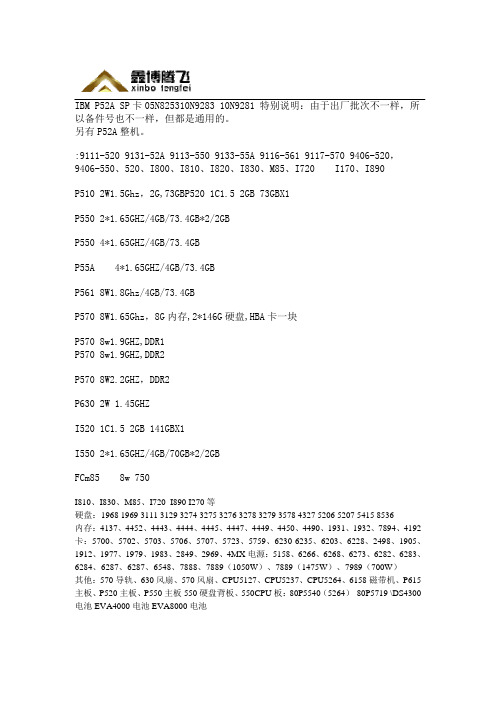
Cisco 350系列产品参数与价格表说明书
4800 Series Adapter
AIR-PC4800
DESCRIPTION
350 Series PC Card w/Integrated Diversity Antenna,128-bitWEP 350 Series PC Card Adapter w/128-bit WEP 40 Pack 350 Series PCI Adapter w/128-bit WEP 10 Pack 350 Series PCI Adapter w/RP-TNC,Dipole Antenna,128-bit WEP 350 Series PC Card w/Dual MMCX Connectors and 128-bit WEP 350 Series PC Card w/Dual MMCX and 128-bit WEP 40 Pack
350 Series Power
AIR-SSI350-J-K9 AIR-PWRINJ=
340 Series Access Point
AIR-BSE342
AIR-AP342E2C AIR-AP342E2R
340 Series Access Point Accessory AIR-ACC5559-072
350 Series Workgroup Bridge w/Captured Antenna / 128-bit WEP 350 Series Workgroup Bridge w/Dual RP-TNC and 128-bit WEP 350 Series 11Mbps, DSSS Bridge w/128-bit WEP 350 Series 11Mbps, DSSS Bridge w/128-bit WEP 350 Series 11Mbps, DSSS Bridge w/128-bit WEP 350 Series Site Survey Kit 350 Series Site Survey Kit 350 Series Site Survey Kit
IBM磁带产品详细参数

数据传输速率
使用全高型和半高型LTO Ultrium 4技术,本机数据传输速率可达120MBps
使用全高型LTO Ultrium 3技术,本机数据传输速率可达80MBps
使用半高型LTO Ultrium 3技术,本机数据传输速率可达60MBps
机架安装
17.6英寸(447.5毫米)x 3.44英寸(87.6毫米)x 29.13英寸(740毫米)
重量
33磅(15公斤)
工作环境
温度
54到95华氏度,12到35摄氏度
相对湿度
20%-80%相对湿度(非冷凝)
功率
100 V交流电压时为1.3 amps;240 V交流电压时为0.7 amps
连接和系统支持
热插拔组件
电源、磁带驱动器
RAID支持
无
系统管理
支持SMI-S
支持的操作系统
OS/400®、V5R2、V5R3或更高版本
AIX 5L™ V5.1、V5.2、V5.3或更高版本
Sun Solaris 8和9
Microsoft® Windows® 2000
Microsoft Windows 2003
HP-UX 11.0、HP-UX 11.11和HP-UX 11.2311
TS3100提供LVD Ultra160、4 Gbps光纤通道和3 Gbps SAS(仅用于LTO4)接口,可连接到IBM System p、IBM System i、IBM System x、RS/6000 SP™、AS/400和IBM Netfinity®系统以及非IBM服务器、工作站和个人计算机上
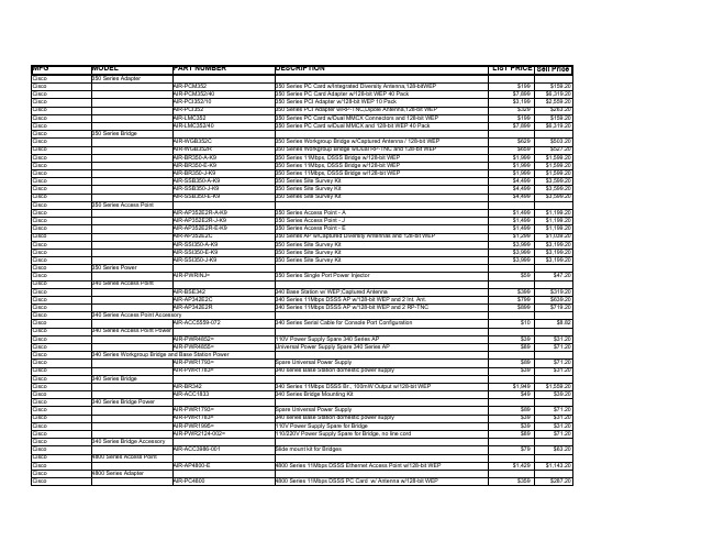
b7s资料
B1S – B10S0.5A SURFACE MOUNT GLASS PASSIVATED BRIDGE RECTIFIERMechanical Data Case: MB-S, Molded PlasticTerminals: Plated Leads Solderable per Single Phase, half wave, 60Hz, resistive or inductive load.For capacitive load, derate current by 20%.CharacteristicSymbol B1S B2S B4S B6S B8S B10S UnitPeak Repetitive Reverse Voltage Working Peak Reverse Voltage DC Blocking Voltage V RRMV RWM V R 1002004006008001000V RMS Reverse VoltageV R(RMS)70140280420560700V Average Rectified Output Current (Note 1) @T A = 40°C Average Rectified Output Current (Note 2) @T A = 40°C I O0.50.8ANon-Repetitive Peak Forward Surge Current 8.3ms Single half sine-wave superimposed on rated load (JEDEC Method)I FSM 30A I 2t Rating for Fusing (t < 8.3ms)I 2t 5.0A 2s Forward Voltage per element @I F = 0.5A V FM 1.0V Peak Reverse Current @T A = 25°C At Rated DC Blocking Voltage @T A = 125°C I RM 5.0500µA Typical Junction Capacitance per leg (Note 3)C j 25pF Typical Thermal Resistance per leg (Note 1)R JA R JL 8520°C/W Operating and Storage Temperature RangeT j , T STG-55 to +150°CNote: 1. Mounted on glass epoxy PC board with 1.3mm 2 solder pad.2. Mounted on aluminum substrate PC board with 1.3mm 2 solder pad.3. Measured at 1.0 MHz and applied reverse voltage of4.0V D.C.WTE0.010.11.0100.20.61.01.4I ,I N S T A N T A N E O U S F O R W A R D C U R R E N T (A )F V ,INSTANTANEOUS FORWARD VOLTAGE (V)Fig.2Typical Forward Characteristics (per leg)F 0.40.81.2 1.60102030351.010I ,P E A K F O R W A R D S U R G E C U R R E N T (A )F S M NUMBER OF CYCLES AT 60HzFig.3Maximum Peak Forward Surge110100110100C ,J U N C T I O N C A P A C I T A N C E (p F )j V ,REVERSE VOLTAGE (V)Junction CapacitanceR0.010.11.01010020406080100120140I ,I N S T A N T A N E O U S R E V E R S E C U R R E N T (A )R µPERCENT OF RATED PEAK REVERSE VOLTAGE (%)Fig.5Typical Reverse Characteristics (per element)0.20.40.60.804080120160I ,A V E R A G E F O R W A R D R E C T I F I E D C U R R E N T (A )(A V )T ,AMBIENT TEMPERATURE (C)Fig.1Output Current Derating Curve A °MARKING INFORMATION RECOMMENDED FOOTPRINTPACKAGING INFORMATIONORDERING INFORMATIONProduct No.Package TypeShipping QuantityB1S-T3Mini Bridge SMD 3000/Tape & Reel B2S-T3Mini Bridge SMD 3000/Tape & Reel B4S-T3Mini Bridge SMD 3000/Tape & Reel B6S-T3Mini Bridge SMD 3000/Tape & Reel B8S-T3Mini Bridge SMD 3000/Tape & Reel B10S-T3Mini Bridge SMD3000/Tape & Reel1. Shipping quantity given is for minimum packing quantity only. For minimum order quantity, please consult the Sales Department.2.To order Lead Free version (with Lead Free finish), add “-LF” suffix to part number above. For example, B1S-T3-LF.Won-Top Electronics Co., Ltd (WTE) has checked all information carefully and believes it to be correct and accurate. However, WTE cannot assume any responsibility for inaccuracies. Furthermore, this information does not give the purchaser of semiconductor devices any license under patent rights to manufacturer. WTE reserves the right to change any or all information herein without further notice.WARNING : DO NOT USE IN LIFE SUPPORT EQUIPMENT. WTE power semiconductor products are not authorized for use as critical components in life support devices or systems without the express written approval.We power your everyday.Won-Top Electronics Co., Ltd.No. 44 Yu Kang North 3rd Road, Chine Chen Dist., Kaohsiung, Taiwan Phone: 886-7-822-5408 or 886-7-822-5410Fax: 886-7-822-5417Email: sales@Internet: 。
NXP mcu
TinyM0核心板电路为LPC111x芯片的最小系统,硬件支持2.54mm间距的 标准排针。用户可以将TinyM0核心板配套自行设计的底板进行产品开发。 ● 支持多款芯片
和16位竞争产品的2至4倍。
Cortex-M0内核
● 32位ARM RISC处理器,16位Thumb指令集; ● 功耗与面积高度优化,设计专用于低成本、低功耗场合; ● 24位SysTick定时器; ● 32位硬件乘法器; ● 中断现场自动保存,有处理决定性、固定延迟的中断能力; ● 系统接口支持小端或字节不变的大端数据访问; ● SWD串行线调试。
LPC1300选型表:
器件型号 LPC1343 LPC1342 LPC1313 LPC1311
Flash (KB) 32 16 32 8
SRAM(KB) 8 4 8 2
USB 2.0 Device Device
-
I2C(Fast+) 1 1 1 1
ADC 8ch/10bit 8ch/10bit 8ch/10bit 8ch/10bit
置的新型开漏工作模式
LPC1100
◎ 四个通用计数器/计数器 ◎ 可编程的看门狗定时器(WDT),带锁死功能 ◎ 系统计时器 ◎ 各外设自带时钟分频器,有利于降低功耗
芯片特色:
Cortex-M0处理器性能 ● Cortex-M0微控制器可以轻松超越高端8位和16位器件的
性能水平; ● 内核额定性能为0.9DMIPS/MHz,相当于与其最接近的8位
ThinkTop D30商品说明书

Signed on behalf of: Alfa Laval Kolding A/S
Global Product Quality Manager
Title
Kolding, Denmark
Place
2022–10–01
Date (YYYY-MM-DD)
DoC Revison_01_102022
Lars Kruse Andersen Name
Lars Kruse Andersen Name
Signature
This Declaration of Conformity replaces Declaration of Conformity dated 2017-03-01
4
1 Declarations of Conformity
UK Declaration of Conformity
2.ays read the manual befor e using the ThinkTop! WARNING Indicates that special procedures must be followed to avoid serious personal injury. CAUTION Indicates that special procedures must be followed to avoid damage to the ThinkTop D30. NOTE Indicates important information to simplify or clarify procedures.
Maintenance:
Always read the technical data thoroughly Always fit the seals between the valve and ThinkTop D30 correctly Never install the ThinkTop D30 before valve or relay is in a safe position Never service the ThinkTop D30 with the valve/actuator under pressure Never clean the ThinkTop D30 with high pressure cleaning equipment Never touch the moving parts if the actuator is supplied with compressed air Never use cleaning agents that will attack the exterior of the ThinkTop D30. Check with your cleaning agent supplier Never clean using Alcohol, Acetone, Chloroform, Methanol, Ammonium chloride and Ammonium Hydroxide etc.
东芝条码打印机 B-SX5T系列 说明书

- 1、下载文档前请自行甄别文档内容的完整性,平台不提供额外的编辑、内容补充、找答案等附加服务。
- 2、"仅部分预览"的文档,不可在线预览部分如存在完整性等问题,可反馈申请退款(可完整预览的文档不适用该条件!)。
- 3、如文档侵犯您的权益,请联系客服反馈,我们会尽快为您处理(人工客服工作时间:9:00-18:30)。
AbstractThis Application Note describes the differences between the CPC710-100+ (DD2) and the CPC710 (DD3.x) versions of the PowerPC Dual PCI/Memory Controller companion chip. The purpose of this note is to provide designers with an overview of the changes and point out performance enhancements and potential programming changes. For a detailed understanding of the operation of the CPC710-133, please refer to the User’s Manual. For a detailed understanding of the physical pin out and electrical specifications, please refer to the Data Sheet. OverviewThe IBM25CPC710 DD3.x is a host bridge that interfaces a PowerPC 60x bus with system memory (SDRAM) and two independent PCI interfaces. It provides arbitration for one to four processors and supports up to two levels of pipelining per processor with 64-byte buffers (maximum of 6 buffers). Use of external slave devices on the 60x bus is also supported andrequires additional external logic. The CPC710 DD3.x supports 60x bus speeds of up to 133MHz at 2.5V. Of course, given signal quality issues with higher bus speeds it is not recommended that the CPU bus run at 133Mhz in configurations that include more than 2 CPUs.The bridge’s two way interleaved memory controller supports SDRAM at 100 or 133 MHz; both single bank and dual bank, PC100, PC133 and registered DIMMs are supported. The memory controller design requires the use of an external multiplexer and two physical DIMMs.The bridge contains two PCI host bus bridges: one provides an interface for a 32-bit, 33 MHz PCI bus for standard and native I/O. This bus supports either 3.3V or 5V logic level devices, and allows attachment of up to 2MB of boot ROM (and up to 256MB of extended boot ROM). The other PCI interface supports a 32- or 64-bit, 33 or 66 MHz PCI bus for high data throughput, but supports only 3.3V logic level devices. This is a change from the previous revision . Burst and non-burst data transfers to memory from the PCI (bridge acts as target on PCI bus) and from memory to the PCI (bridge acts as master on PCI bus) are supported; data transfers directly between PCI-32 and PCI-64 are not supported . This is a change from the previous revision.A single channel DMA controller provides support for large data transfers betweenmemory and the PCI busses. DMA to and from the CPU bus to memory, or between PCI-32 and PCI-64 is not supported. This is a change from the previous revision.IBM25CPC710 Bridge Chip:Enhancements and Changes in theDD3.x revisionsPowerPC TMApplications IBM Microelectronics Research Triangle Park, NC ppcsupp@ Processor Interface:v Voltage Level and Bus Speed DifferencesØ The CPC710 DD3.x revision supports 60x bus operation at speeds of up to 133MHz, at an I/O voltage of 2.5V. This interface voltage level is supported on the PPC750L, 750CX,and 750CXe processors.This is a change from the previous revision.v I/O Signal New FunctionalityØ Set bit 18 of 60x Bus Arbiter register (system register CPC0_ABCNTL) to 1 to allow the signal level of SYS_TA_ to be confirmed and held at a high logic level (after precharging) as soon as the CPC710 DD3.x exits the RESET state. This is to allow for properoperation in systems with high loads on the CPU bus.v I/O Signal Additional Functionality for 4-way Processor Support Ø Coming out of reset, the 60x bus arbitration logic of the CPC710 DD3.x defaults to the same dual processor mode used in the CPC710 DD2. To enable 4-way arbitration, theMaster CPU should set chip control register CPC0_ABCNTL [17] to a “1”. Then theSYS_HRESET2_, SYS_HRESET3_, SYS_SRESET2_ and SYS_SRESET3_ signals will go inactive, allowing CPUs 2 and 3 to exit the reset state.Ø The two Reset registers CPC0_RSTR and CPC0_SRST have been modified to include bits to support program control operation of hard and soft reset signals for the additionalprocessors.§ Connectivity Reset Register bits CPC0_RSTR [4:5] controls signals SYS_HRESET2_ and SYS_HRESET3_ respectively. CPU Soft Reset Register bits CPC0_SRST [4:5]controls signals SYS_SRESET2_ and SYS_SRESET3_ respectively§ The CPC0_PIDR Register has been modified to allow identification of each of the 4 processors; if CPC0_PIDR [24:31] is read as 'h00’ it indicates the Processorcorresponding to BR0_/BG0_ is active. Valid values for these bits are:• = 0x00==> Processor corresponding to BR0_/BG0_• = 0x01 ==> Processor corresponding to BR1_/BG1_• = 0x02 ==> Processor corresponding to BR2_/BG2_• = 0x03 ==> Processor corresponding to BR3_/BG3_v I/O Signals for 4-way Processor SupportØ The signals SYS_MCP0: 3 are used to indicate to the CPUs that the CPC710 has detected an error condition and a machine check is required. To help reduce pin count,output signals SYS_MCP2_ and SYS_MCP0_ are generated from one internal signalsource. SYS_MCP3_ and SYS_MCP1_ also share a common internal signal source.Ø The System Error Status Register has not been modified and only errors that occur with Processor 0 or 1 can be detected and reported.Memory Interface:v Extended SDRAM AddressingØ The signal MADDR13 has been added to support the following additional SDRAM organizations:§ 13-12-2, 14-9-2, 14-10-2, 14-11-2, 14-12-2§ Register SDRAM0_MCER [26:29] is used to select the SDRAM organization; refer to the CPC710-133 User’s Manual for more information.v Extended Memory SizeØ The Memory controller has been modified to support up to six banks of dual DIMM interleaved 72-bit memory, for a total memory addressing range of 3.5GB. The memorycontroller now allows configuration of bank sizes up to 4GB per bankThe choice of 4MB to 1GB (same as the CPC710-100+) or 4MB to 4GB is made withSDRAM0_MCCR [8].§ If SDRAM0_MCCR [8] = 1 bank size range is from 4MB to 1GB§ If SDRAM0_MCCR [8] = 0 bank size range is from 4MB to 4GB§ Refer to the CPC710-133 User’s Manual for more information.v Supported Memory TypesØ Supports JEDEC standard PC100 and PC133 SDRAMs, both single bank and dual bank.Ø EDO memory is no longer supported on the CPC710 with the DD3.x revision.Ø All types of registered DIMMs are now supported on the CPC710 with the DD3 version.New programming bits are defined in register SDRAM0_MCCR0 to support registeredDIMMS.§ Setting SDRAM0_MCCR [16] = 1 adds one additional clock cycle to the internal sequencer signals for read operations of registered DIMMs.§ Setting SDRAM0_MCCR [19] =1 shifts the following signals by one clock cycle: MUX_SEL, MUX_CLKEN1B_, MUX_CLKEN2B_§ Setting SDRAM0_MCCR [21] = 1 allows the data to be written to the memory to be held valid for an additional clock cycle.§ Setting SDRAM0_MCCR [22] = 1 shifts the following signals by one clock cycle: MUX_CLKENA2_, MUX_OEB_, SDRAS0_, SDRAS1_, SDCAS0_, SDCAS1_, WE0_,WE1_, MADDR0_ODD, MADDR0_EVEN, MADDR1-13, BS0 and BS1v Maximum Number of Memory Banks Decreased from 8 to 6Ø CPC710 DD3.x revision does not support the use of registers MCER6 and MCER7.These registers were present in the CPC710-100+ DD2 version.Ø Internal memory controller logic no longer generates SDCS12_ through SDCS15_. These signals were present in the CPC710-100+ DD2 version. The multiplexing capabilitiesdefined in register SDRAM0_MCCR [11:15] have been modified from the usage inCPC710 DD2 revision. This multiplexing allows for support of SDRAM speeds up to 133MHz. The higher speed is attained by limiting the loading (number of SDRAM packages) on each SDCS signal.§ New encoding:• If SDRAM0_MCCR [11] = 1 signals SDCS_[0:3] use I/O pins SDCS_[4:7]• If SDRAM0_MCCR [12] = 1 signals SDCS_[0:3] use I/O pins SDCS_[8:11]• SDRAM0_MCCR [13] is no longer used• If SDRAM0_MCCR [14] = 1 signals SDQM use I/O pins SDRAS1_, SDCAS1_ and WE1_• If SDRAM0_MCCR [15] = 1 signals SDQM uses I/O pins PCG_ARBv Extended Addressing of PCI MemoryØ System memory addressing range increased from 2GB to 4GB. The standard addressing capability is 2GB; with the size defined by bits 24-31 of PCI local registersPCILx_PSSIZE. The address extension is implemented by setting bit 27 of chip controlregister CPC0_PGCHP. In this case, the FINE option for selection of less than1MBgranularity (enabled in CPC710-100+ dd2 in the memory write protection registerSDRAM0_MWPR) is not available.PCI Interfaces:v The PCI-64 Interface is no Longer 5 Volt TolerantØ The I/O drivers used on the CPC710 DD3.x PCI-64 interface no longer support 5V logic levels – users must attach only 3.3V devices to the PCI-64 bus. This is a change from the previous revision.v PCI-32 Interface Now Supports External Arbiter UsageØ The PCI-32 interface now allows use of an external PCI bus arbiter. A method similar to that used for disabling the PCI-64 internal arbiter is used to for disabling the PCI-32internal arbiter.§ At power on, after activation of the POWERGOOD signal, the signal P_REQ2_ is sampled. This initial sampling is done while PLL_RESET is active, and isindependent of activation of the PCI clock on the bus. If the signal level is 0, theinternal arbiter for the PCI-32 bus is disabled. Bit 16 of chip control registerCPC0_PGCHP can be read to determine the detected arbitration mode; a “0”indicates the internal arbiter is in use, and a “1” indicates an external arbiter.§ For the PCI-64 interface, the signal sampled after activation of the POWERGOOD signal is G_REQ2_. This initial sampling is done while PLL_RESET is active, andis independent of activation of the PCI clock on the bus. Bit 9 of chip controlregister CPC0_PGCHP can be read to determine the detected arbitration mode; a“0” indicates the internal arbiter is in use, and a “1” indicates an external arbiter.Ø NOTE: Because the FLASH interface is present on the PCI-32 bus, configurations using an external PCI bus arbiter must prevent any external PCI-32 transactions from interfering or pre-empting FLASH transactions.Power and PLL:v New Supply VoltagesØ 60x bus voltage level now 2.5V. To support the I/O interfaces on the PPC750CX/CXe (as well as the PPC750L) the 60x bus interface logic is now 2.5V. This is a change from the previous revision.Ø VDD (core logic) is also 2.5V.Ø OVDD (I/O logic) for SDRAM and PCI interfaces is 3.3V.Ø The AVDD (PLL) is 2.5V.§ AVDD is the voltage supply pin to the analog circuits in the PLL. Noise on AVDD will cause phase jitter at the output of the PLL. To provide isolation from the noisyinternal digital VDD signal, AVDD is brought to a package pin. If little noise isexpected at the board level, then AVDD can be connected directly to the digital VDDplane. In most circumstances, however, it is prudent to place a filter circuit on AVDD;refer to the CPC710 DD3.x User’s Manual for more information.Ø The PLL is now set up and controlled by external signals PLL_RANGE [1:0] and 6 external signals PLL_TUNE [5:0] instead of PLL133 and PLL_TUNE [1:0]. This is achange from the previous revision.Packaging Changes:v FC-PBGA Package instead of CBGAØ The CPC710 DD3.x is offered in a 35mm 728 pin FC-PBGA (Flip Chip Plastic Ball Grid Array) package. This is a change from the previous revision – the DD3.x is notpin/package compatible with the DD2.Refer to the CPC710-133 PCI Bridge and Memory Controller Datasheet for more details on the physical packaging.v I/O Pinout Deletions:The following I/Os are no longer present on the DD3 revision:INTERFACE SIGNAL NAME IMPACTMemory Interface SDCS_12, SDCS_13, SDCS_14,SDCS_15SDRAS_2, SDRAS_3SDCAS_2, SDCAS_3WE_2, WE_3Changes to the memory interface.Refer to Chapter 6 Of User’sManual for more details.PCI 32-bit Interface P_GNT_6, P_GNT_5, P_GNT_4,P_REQ_6, P_REQ_5, P_REQ_4Decreases number of PCI devicessupported by the internal busarbiter, unless multiplexed (seebelow).PCI 32-bitInterfaceP_ISA_MASTERPCI 32-bit Interface P_CFG [0:2] CFGA [13:11] no longer drivenoffchip (used for save loads on PCIbus)PCI 64-bit Interface G_CFG [0:2] CFGA [13:11] no longer drivenoffchipClock Inputs PLL_133, PLN_RTC_CLOCK DD3 has new strapping options.Timers now controlled only byPCI32 clock.Test Signals CE1_A, CE1_B, CE1_C1, CE1_C2, DI1,DI2, CE0_IO, RI, SCAN_GATE,TESTIN, CE_TRST, TESTOUT Signals used only by manufacturing test.v I/O Pin Additions:The following I/Os are new on the DD3 revision:INTERFACE SIGNAL NAME IMPACT60x bus Interface SYS_BG2_, SYS_BG3_, SYS_MCP2,SYS_MCP3, SYS_HRESET2,SYS_HRESET3, SYS_SRESET2,SYS_SRESET3New for 4-way CPU support 60x bus Interface SYS_TA_HITMemory Interface MADDR13 Used for newer memory sizesClock Inputs PLL_RANGE0, PLL_RANGE1,PLL_TUNE2, PLL_TUNE3, PLL_TUNE4,PLL_TUNE5 New; used for setup and control of PLLv I/O Pins Multiplexed:The following I/Os are multiplexed on the DD3 revision:INTERFACE PIN FUNCTION OPTION REGISTER BIT TO USETO SELECT FUNCTION Memory Interface SDRAS_1 becomes SDQM SDRAM0_MCCR [14] = 1 Memory Interface SDCAS_1 becomes SDQM SDRAM0_MCCR [14] = 1 Memory Interface WE_1 becomes SDQM SDRAM0_MCCR [14] = 1 Memory Interface G_ARB becomes SDQM SDRAM0_MCCR [15] = 1 60x bus Interface DRAMREQ_ becomes NODLK_ CPC0_PGCHP [20] = 0 60x bus Interface DRAMGNT_ becomes DLK_ CPC0_PGCHP [20] = 0 PCI 64-bit Interface G_REQ_7 becomes P_REQ_6 CPC0_PGCHP [23] = 1 PCI 64-bit Interface G_GNT_7 becomes P_GNT_6 CPC0_PGCHP [23] = 1 PCI 64-bit Interface G_REQ_6 becomes P_REQ_5 CPC0_PGCHP [22] = 1 PCI 64-bit Interface G_GNT_6 becomes P_GNT_5 CPC0_PGCHP [22] = 1 PCI 64-bit Interface G_REQ_5 becomes P_REQ_4 CPC0_PGCHP [21] = 1 PCI 64-bit Interface G_GNT_5 becomes P_GNT_4 CPC0_PGCHP [21] = 1 Hardware ID Changes for DD3.0 revision:v PCI-32 revision ID in PCIC0_REVID = x’03v PCI-64 revision ID in PCIC1_REVID = x’03v EC Level in CPC0_UCTL [24:31] = x’a0Performance Enhancements and Improvements:v The CPC710 DD3.x revision has improvements to support PCI Long Burst Write operations and improvements in the deadlock prevention circuits. These enhancements can be selected by programming select bits in PCI local registers PCILx_PSWCR and PCILx_DLKCTRL.Ø Crossing a 4K boundary during burst operations results in a stop on the PCI bus. By default operation, snooping is done on the current PCI master’s address. A new option is provided to allow for anticipation logic to snoop ahead to the next address. Set PCI local register PCILx_PSWCR [17] to “1” to enable the snoop ahead logic.Ø There have been several changes to the deadlock avoidance logic. The CPC710 DD2 errata #8 and #9, relating to defects in the deadlock circuitry, have been fixed in theCPC710 DD3.x revision. In addition, there are three improvements that can be selectedby setting the appropriate bits.§ PCILx_DLKCTRL [27] – when set to “0” enables the erratum #8 correction logic to prevent potential deadlock in multiprocessor configurations when one CPU isattempting a PCI read. For more details on the erratum, please read the CPC710DD2 Errata List. Setting this bit to “1” disables the correction logic.§ PCILx_DLKCTRL [28] – when set to “0” enables the erratum #9 correction logic to function correctly when the programmed value in the PCI local registerPCILx_DLKCTRL [8:15] is greater than 0x0F. Setting this bit to a “1” disables thecorrection logic.§ PCILx_DLKCTRL [29] - when set to “1” results in the following: When a read is already in progress to an address defined in the deadlock avoidance address range,an ARTRY will be generated for all accesses except the access to the main memoryfor that read. Setting this bit to a “0” disables this logic. The default state for this bit isrecommended, as other methods of deadlock avoidance have proven to be flexibleenough to resolve problems without use of this logic.§ PCILx_DLKCTRL [30] - when set to “0” results in the following: The processor ID is taken into account in the deadlock avoidance logic. Setting this bit to a “1” causes thedeadlock logic to ignore the processor ID.§ PCILx_DLKCTRL [31] - when set to “0” results in the following: The deadlock avoidance logic using the signals MEMREQ/MEMACK and DLK/NODLK are masked.Setting this bit to a “1” causes the deadlock logic to generate these signals as usual. Please send questions or comments about this document to Embedded PowerPC Technical Support: ppcsupp@IBM CorporationPowerPC Embedded Processor SolutionsApplications EngineeringResearch Triangle Park, NC 27709(c) Copyright International Business Machines Corporation 2001All Rights ReservedPrinted in the United States of America November 2001The following are trademarks of International Business Machines Corporation in the United States, or other countries, or both:IBM PowerPC IBM LogoOther company, product and service names may be trademarks or service marks of others.All information contained in this document is subject to change without notice. The products described in this document are NOT intended for use in implantation or other life support applications where malfunction may result in injury or death to persons. The information contained in this document does not affect or change IBM product specifications or warranties. Nothing in this document shall operate as an express or implied license or indemnity under the intellectual property rights of IBM or third parties. All information contained in this document was obtained in specific environments, and is presented as an illustration. The results obtained in other operating environments may vary.THE INFORMATION CONTAINED IN THIS DOCUMENT IS PROVIDED ON AN "AS IS" BAS IS. In no event will IBM beliable for damages arising directly or indirectly from any use of the information contained in this document.。