MAX263BEPI中文资料
MAX9632-MAX9633低噪音
MAX9632/MAX9633 低噪音
Maxim 的新轨至轨运算放大器提供高电压性能在低频率,精确的规格,高收益,能够在工业应用精密的信号调理。
位于美国加州Sunnyvale,2010 年11 月9 日,MAXIM 集成产品公司(NASDAQ:MXIM)推出MAX9632/MAX9633 的36V,低噪音,低失真精密运算放大器。
在Maxim 的高电压,精密运算放大器新系列的第一个器件,MAX9632/MAX9633 的设计采用了一个专有的高速互补BiCMOS 工艺
(CB5HV)。
这个高电压模拟工艺优化交流优秀的动态性能,超低噪声,工作电压范围宽,低漂移信号调理。
MAX9632/MAX9633 目标的工业数据采集系统的精度要求在低频信号调理。
在MAX9632 是单运放具有超低输入电压噪声密度0.94nV /,低偏移的125μV(最大值),和偏移量温度系数的0.5μV/° C(最大)。
在MAX9633 是一款双用的3nV 输入电压噪声密度运算放大器/,对200μ偏移(最大)一,和偏移量温度系数的0.9μV/° C(最大)。
这两款器件提供高规格的信号保真度和总谐波失真调节优于-一三六分贝,能够在专业音响设备和高端测试和仪器仪表应用。
增益带宽积(GBWP)是典型的MAX9632 和MAX9633 27MHz 时为55MHz 的。
这可用带宽,慷慨的4.5V 至36V 工作电压范围,典型的三点九毫安(MAX9632)电流消耗相结合,。
263系列金属螺杆尖耐抗电尖耐抗电尖通螺杆类型环形编码器说明书
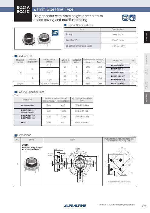
Through shaft type
Horizontal
Horizontal
—
12/12
12/24 12/12
9/18 15/30
Ring type
— 15/30
Features
W
Dimensions (mm)
D
H
Operating temperature range
Operating life Automotive use Life cycle (availability)
300V AC for 1minute or 360V AC for 2s
300V AC for 1minute or 360V AC for 1s
—
7±5mN・m 12±5mN・m 16±7mN・m
—
17±8mN・m(Initial) 12+− 74mN・m(After reflow)
100N
Shaft configuration
1
Style
5-3.5 9
4 Mounting surface
3 2
120°
ø21.6
C ø12.2
AB 1
2-8
120°
0.7
2-10.4 120°
Unit:mm
PC board mounting hole dimensions (Viewed from mounting side)
22.3
3
˃˃
˃ $ ˃ $
˃˃
"# "#
EC21A Actuator length 15mm 9 pulse/18 detent
MAX26_系列数字编码式滤波器的使用方法

第32卷第3期2000年5月四川大学学报(工程科学版)J OURNA L OF SICHUAN UNIVERSITY(ENGINEERING SCIENCE EDITIO N)Vol.32No.3May2000文章编号:1009-3087(2000)03-0058-03MAX26系列数字编码式滤波器的使用方法羿飒,田远富(四川大学电气信息学院,成都610065)摘要:主要介绍MAX26系列4阶开关电容滤波器的使用方法。
给出了其引脚图及各引脚功能,指明了其使用的电压频率范围,说明了如何进行模式选择以及在不同模式下频率编码输入端和Q值编码输入端的设定。
总结了其性能优点,特别指出了实际应用中应注意的问题。
并在理论计算的基础上,设计出用MAX267实现中心频率220 Hz,带宽6.875Hz的带通滤波电路,进一步通过实验测试,验证了MAX26系列数字滤波器的滤波效果。
关键词:数字滤波器;中心频率;带宽中图分类号:TN713.92文献标识码:AUsage of MAX26Series Digital FilterY I Sa,TIAN Y uan-f u(College of Electrical Informati on,Sichuan Uni v.,Chengdu610065,Chi na)Abstract:This paper mainly introduces the operation methods of the MAX26series four-order on-off capacitance filter. We provide the pin description,show clearly the applicable range of volt and frequency,demonstrate how to select mode and set up the frequency-encode input and Q value-encode input under each mode,summarize the virtues of properties, especially point out the problems which should be a ware of in actual applications.Then on the basis of theoretic calcula-tion,we have designed the band-pass filter circuit,which can realize center frequenc y220Hz,bandwidth6.875Hz by using MAX267.Through experimental test,take further steps to verify the filter effect of MAX26series digital filter. Key words:digital filter;center frequenc y;bandwidthMAX263/264/267/268是MAXIM公司新推出的4种应用非常广泛的4阶开关电容滤波器。
MAX262中文资料
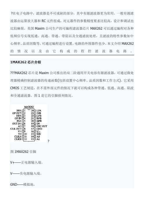
?在电子电路中,滤波器是不可或缺的部分,其中有源滤波器更为常用。
一般有源滤波器由运算放大器和RC元件组成,对元器件的参数精度要求比较高,设计和调试也比较麻烦。
美国Maxim公司生产的可编程滤波器芯片MAX262可以通过编程对各种低频信号实现低通、高通、带通、带阻以及全通滤波处理,且滤波的特性参数如中心频率、品质因数等,可通过编程进行设置,电路的外围器件也少。
本文介绍MAX262的情况以及由它构成的程控滤波器电路。
1MAX262芯片介绍???MAX262芯片是Maxim公司推出的双二阶通用开关电容有源滤波器,可通过微处理器精确控制滤波器的传递函数(包括设置中心频率、品质因数和工作方式)。
它采用CMOS工艺制造,在不需外部元件的情况下就可以构成各种带通、低通、高通、陷波和全通滤波器。
图1是它的引脚排列情况。
?图1MAX262引脚V+——正电源输入端。
V-——负电源输入端。
GND——模拟地。
CLKA——外接晶体振荡器和滤波器A部分的时钟输入端,在滤波器内部,时钟频率被2分频。
CLKB——滤波器B部分的时钟输入端,同样在滤波器内部,时钟频率被2分频。
CLKOUT——晶体振荡器和R-C振荡的时钟输出端。
OSCOUT——与晶体振荡器或R-C振荡器相连,用于自同步。
INA、INB——滤波器的信号输入端。
BPA、BPB——带通滤波器输出端。
LPA、LPB——低通滤波器输出端。
HPA、HPB——高通、带阻、全通滤波器输出端。
WR——写入有效输入端。
接V+时,输人数据不起作用;接V-时,数据可通过逻辑接口进入一个可编程的内存之中,以完成滤波器的工作模式、f0及Q的设置。
此外,还可以接收TTL电平信号,并上升沿锁存输人数据。
A0、A1、A2、A3——地址输人端,可用来完成对滤波器工作模式、f0和Q的相应设置。
D0、D1——数据输入端,可用来对f0和Q的相应位进行设置。
OPOUT——MAX262的放大器输出端。
OPIN——MAX262的放大器反向输入端。
MAX2630-MAX2633中文资料
_______________General DescriptionThe MAX2630/MAX2631/MAX2632/MAX2633 are low-voltage, low-noise amplifiers for use from VHF to microwave frequencies. Operating from a single +2.7V to +5.5V supply, these devices have a flat gain response to 900MHz. Their low noise figure and low supply current make them ideal for receive, buffer, and transmit IF applications.The MAX2630/MAX2631 are biased internally, eliminat-ing the need for external bias resistors or inductors. The MAX2632/MAX2633 have a user-selectable supply cur-rent, which can be adjusted by adding a single external resistor. This allows customized output power and gain according to specific applications requirements. The MAX2631/MAX2633 feature a shutdown pin that allows them to be powered down to less than 1µA supply cur-rent. Aside from a single bias resistor required for the MAX2632/MAX2633, the only external components needed for this family of amplifiers are input and output blocking capacitors and a V CC bypass capacitor.The MAX2630 comes in a 4-pin SOT143 package, re-quiring minimal board space. The MAX2631/MAX2632come in small 5-pin SOT23 packages. The MAX2633comes in a 6-pin SOT23 package.________________________ApplicationsPersonal Communicating Systems Cordless Phones Global Positioning Systems Cellular Phones Wireless Local Area Networks ISM Radios Wireless Local Loops TV Tuners Land Mobile RadiosSet-Top Boxes____________________________Featureso Single +2.7V to +5.5V Operation o Internally Biased (MAX2630/MAX2631)o Adjustable Bias (MAX2632/MAX2633)o 6.6mA Supply Current (insensitive to supply voltage)o 1µA Shutdown Current (MAX2631/MAX2633)o 3.7dB Noise Figure o 13.4dB Gaino Ultra-Small SOT PackagesMAX2630–MAX2633VHF-to-Microwave, +3V ,General-Purpose Amplifiers________________________________________________________________Maxim Integrated Products1_________________Pin Configurations__________Typical Operating Circuit______________Ordering Information19-1181; Rev 1; 7/97*The first two letters in the SOT top mark identify the part,while the remaining two letters are the lot-tracking code.For free samples & the latest literature: , or phone 1-800-998-8800.For small orders, phone 408-737-7600 ext. 3468.M A X 2630–M A X 2633VHF-to-Microwave, +3V ,General-Purpose Amplifiers 2_______________________________________________________________________________________ABSOLUTE MAXIMUM RATINGSELECTRICAL CHARACTERISTICS(V CC = +3V, Z 0= 50Ω, f IN = 900MHz, R BIAS = 10k Ω(MAX2632/MAX2633), V SHDN = V CC (MAX2631/MAX2633), T A = +25°C, unless otherwise noted.)Stresses beyond those listed under “Absolute Maximum Ratings” may cause permanent damage to the device. These are stress ratings only, and functional operation of the device at these or any other conditions beyond those indicated in the operational sections of the specifications is not implied. Exposure to absolute maximum rating conditions for extended periods may affect device reliability.Note 1:Guaranteed by design and characterization.V CC to GND................................................................-0.3V to 6V Input Power.........................................................................5dBm OUT Current.....................................................................±12mA IN to GND Voltage...................................................-1.2V to 1.2V Bias to GND Voltage....................................................0.0V to 3V Voltage at SHDN Input(MAX2631/MAX2633)............................-0.3V to (V CC + 0.3V)Current into SHDN Input (MAX2631/MAX2633).................100µAContinuous Power Dissipation (T A = +70°C)SOT143 (derate 4mW/°C above +70°C).....................320mW SOT23-5 (derate 7.1mW/°C above +70°C).................571mW SOT23-6 (derate 7.1mW/°C above +70°C).................571mW Operating Temperature Range ...........................-40°C to +85°C Junction Temperature......................................................+150°C Storage Temperature Range.............................-65°C to +150°C Lead Temperature (soldering, 10sec).............................+300°CMAX2630–MAX2633VHF-to-Microwave, +3V ,General-Purpose Amplifiers_______________________________________________________________________________________3__________________________________________Typical Operating Characteristics(V CC = +3V, V SHDN = V CC (MAX2631/MAX2633), Z 0= 50Ω, f IN = 900MHz, R BIAS = 10k Ω(MAX2632/MAX2633), T A = +25°C, unless otherwise noted.)108642023456SUPPLY CURRENT vs. SUPPLY VOLTAGEV CC (V)I C C (m A )252015105005.02.510.015.0MAX2632/MAX2633GAIN vs. SUPPLY CURRENTI CC (mA)G A I N (d B )7.512.52016128400.10.30.71.11.31.5GAIN vs. FREQUENCY AND VOLTAGEFREQUENCY (GHz)G A I N (d B )0.50.9-5.0-7.5-10.0-12.5-15.00.10.30.71.11.31.5OUTPUT 1dB COMPRESSIONPOWER vs. FREQUENCY AND TEMPERATUREFREQUENCY (GHz)P -1 (d B m )0.50.92016128400.10.30.71.11.31.5GAIN vs. FREQUENCYAND TEMPERATUREFREQUENCY (GHz)G A I N (d B )0.50.9-5.0-7.5-10.0-12.5-15.00.10.30.71.11.31.5OUTPUT 1dB COMPRESSIONPOWER vs. FREQUENCY AND VOLTAGEFREQUENCY (GHz)P -1 (d B m )0.50.9-4-8-12-16-202.57.512.515.0MAX2632/MAX2633OUTPUT 1dB COMPRESSION POWER vs. SUPPLY CURRENTI CC (mA)P -1 (d B m )5.010.05432100.10.30.50.91.11.5NOISE FIGURE vs. FREQUENCYM A X 2630-8FREQUENCY (GHz)N O I S E F I G U R E (d B )0.71.3M A X 2630–M A X 2633VHF-to-Microwave, +3V ,General-Purpose Amplifiers 4_____________________________________________________________________________________________________________________________________________________Pin Description15129630110100MAX2632/MAX2633SUPPLY CURRENT vs. R BIASR BIAS (k Ω)I C C (m A)00.010.030.020.040.05-40-2020406080MAX2631/MAX2633SHUTDOWN SUPPLY CURRENTvs. TEMPERATURETEMPERATURE (°C)S H U T D O W N I C C (µA )5:14:13:12:11:10.10.30.7 1.1 1.3 1.5VOLTAGE STANDING-WAVE RATIO vs. FREQUENCYFREQUENCY (GHz)V S W R0.50.9____________________________Typical Operating Characteristics (continued)(V CC = +3V, V SHDN = V CC (MAX2631/MAX2633), Z 0= 50Ω, f IN = 900MHz, R BIAS = 10k Ω(MAX2632/MAX2633), T A = +25°C, unless otherwise noted.)MAX2630–MAX2633VHF-to-Microwave, +3V ,General-Purpose Amplifiers_______________________________________________________________________________________5Table 1a. Typical Scattering Parameters(V CC = +3V, V SHDN = V CC , Z 0= 50Ω, R BIAS = 10k Ω, T A = +25°C.)M A X 2630–M A X 2633VHF-to-Microwave, +3V ,General-Purpose Amplifiers 6_______________________________________________________________________________________Table 1b. MAX2633 Typical Scattering Parameters(V CC = +5V, V SHDN = V CC , Z 0= 50Ω, R BIAS = 10k, T A = +25°C.)MAX2630–MAX2633VHF-to-Microwave, +3V ,General-Purpose Amplifiers_______________________________________________________________________________________7_______________Detailed DescriptionThe MAX2630–MAX2633 are broadband amplifiers with 3dB bandwidth greater than 1GHz. Their small size and internal bias circuitry make them ideal for applications where board space is limited. The MAX2632/MAX2633have a user-selectable bias current that allows the user to set both gain and output power for a particular appli-cation, and the MAX2631/MAX2633 incorporate shut-down capability.__________Applications InformationExternal ComponentsThe MAX2630–MAX2633 are easy to use, as shown in the Typical Operating Circuit and Figures 1, 2 and 3. Input and output series capacitors may be necessary to block DC bias voltages generated by the amplifiers from inter-acting with adjacent circuitry. These capacitors must be large enough to contribute negligible reactance in a 50Ωsystem at the minimum operating frequency. Use the fol-lowing equation to calculate their minimum value:where f (in megahertz) is the minimum operating frequency.The V CC pin must be RF bypassed for correct opera-tion. To accomplish this, connect a capacitor between the V CC pin and ground, as close to the package as is practical. Use the same equation given above (for DC-blocking capacitor values) to calculate the minimum capacitor value. If the PC board has long V CC lines,additional bypassing may be necessary. This can be done farther away from the package, if needed.Proper grounding of the GND pin is essential. If the PC board uses a topside RF ground, connect it directly to the GND pin. For a board where the ground plane is not on the component side, the best technique is to con-nect the GND pin to it with a plated through-hole close to the package.An on-chip buffer at the MAX2631/MAX2633’s SHDN pin makes bypassing this pin unnecessary except in very noisy applications. When RF filtering is needed,use a bypass capacitor similar to the one used on V CC .Since negligible current flows into this pin, additional RF filtering may be done with a series resistor.To set the MAX2632/MAX2633’s supply current,connect a resistor from the BIAS pin to ground. To estimate the value of this resistor, refer to the graph Supply Current vs. R BIAS in the Typical Operating Characteristics .C BLOCK =53,000f(pF)M A X 2630–M A X 2633VHF-to-Microwave, +3V ,General-Purpose Amplifiers 8_______________________________________________________________________________________Figure 4. MAX2630 Example PC Board LayoutFigure 5. MAX2631 Example PC Board LayoutFigure 7. MAX2633 Example PC Board LayoutFigure 6. MAX2632 Example PC Board Layout PC Board Layout ExampleExample PC board layouts are given in Figures 4 to 7.They use FR-4 with a 31mil layer thickness between the RF lines and the ground plane. The boards satisfy all of the above recommendations.MAX2630–MAX2633VHF-to-Microwave, +3V ,General-Purpose Amplifiers_______________________________________________________________________________________9__________________________________________________Tape-and-Reel Information___________________Chip InformationTRANSISTOR COUNT: 199M A X 2630–M A X 2633VHF-to-Microwave, +3V ,General-Purpose Amplifiers 10______________________________________________________________________________________________________________________________________________Package InformationMAX2630–MAX2633VHF-to-Microwave, +3V ,General-Purpose Amplifiers ______________________________________________________________________________________11___________________________________________Package Information (continued)M A X 2630–M A X 2633VHF-to-Microwave, +3V ,General-Purpose Amplifiers___________________________________________Package Information (continued)Maxim cannot assume responsibility for use of any circuitry other than circuitry entirely embodied in a Maxim product. No circuit patent licenses are implied. Maxim reserves the right to change the circuitry and specifications without notice at any time.12____________________Maxim Integrated Products, 120 San Gabriel Drive, Sunnyvale, CA 94086 408-737-7600©1997 Maxim Integrated Products Printed USA is a registered trademark of Maxim Integrated Products.。
金库利模型2635A 2636A系统源电流器说明书
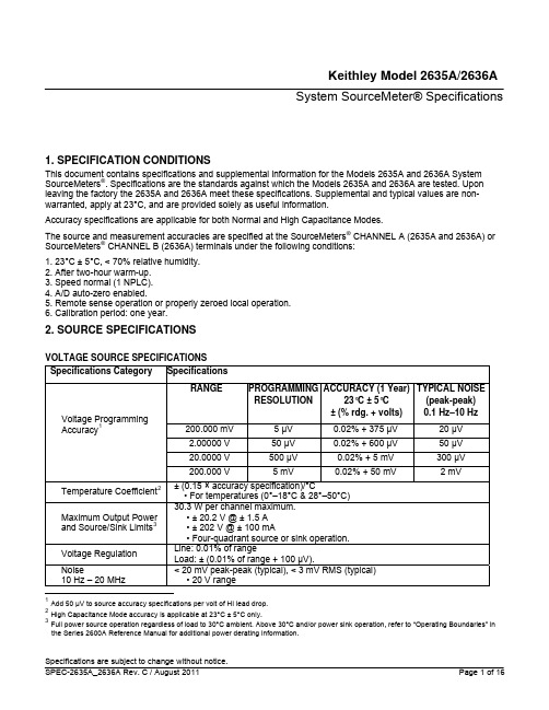
Keithley Model 2635A/2636A System SourceMeter® Specifications1.SPECIFICATION CONDITIONSThis document contains specifications and supplemental information for the Models 2635A and 2636A System SourceMeters ®. Specifications are the standards against which the Models 2635A and 2636A are tested. Upon leaving the factory the 2635A and 2636A meet these specifications. Supplemental and typical values are non-warranted, apply at 23°C, and are provided solely as useful information.Accuracy specifications are applicable for both Normal and High Capacitance Modes.The source and measurement accuracies are specified at the SourceMeters ® CHANNEL A (2635A and 2636A) or SourceMeters ® CHANNEL B (2636A) terminals under the following conditions: 1.23°C ± 5°C, < 70% relative humidity.2.After two-hour warm-up.3.Speed normal (1 NPLC).4.A/D auto-zero enabled.5.Remote sense operation or properly zeroed local operation.6.Calibration period: one year.2.SOURCE SPECIFICATIONSVOLTAGE SOURCE SPECIFICATIONSSpecifications Category SpecificationsRANGE PROGRAMMING RESOLUTION ACCURACY (1 Year) 23°C ± 5°C± (% rdg. + volts) TYPICAL NOISE(peak-peak) 0.1 Hz–10 Hz 200.000 mV 5 µV 0.02% + 375 µV 20 µV 2.00000 V 50 µV 0.02% + 600 µV 50 µV 20.0000 V 500 µV 0.02% + 5 mV 300 µV Voltage Programming Accuracy 1200.000 V5 mV0.02% + 50 mV2 mVTemperature Coefficient 2 ± (0.15 × accuracy specification)/°C•For temperatures (0°–18°C & 28°–50°C)Maximum Output Powerand Source/Sink Limits 3 30.3 W per channel maximum. •± 20.2 V @ ± 1.5 A •± 202 V @ ± 100 mA•Four-quadrant source or sink operation.Voltage Regulation Line: 0.01% of rangeLoad: ± (0.01% of range + 100 µV).Noise10 Hz – 20 MHz< 20 mV peak-peak (typical), < 3 mV RMS (typical) •20 V range1Add 50 µV to source accuracy specifications per volt of HI lead drop.2High Capacitance Mode accuracy is applicable at 23°C ± 5°C only.3Full power source operation regardless of load to 30°C ambient. Above 30°C and/or power sink operation, refer to “Operating Boundaries” in the Series 2600A Reference Manual for additional power derating information.Model 2635A/2636ASystem SourceMeter® SpecificationsSpecifications Category SpecificationsCurrentLimit/Compliance 4 Bipolar current limit (compliance) set with single value. Minimum value is 100 pA. Accuracy is the same as current source. Overshoot< ± (0.1% + 10 mV) (typical )•Step size = 10% to 90% of range, resistive load, maximum current limit/compliance.Guard Offset Voltage< 4 mV•Current < 10 mACURRENT SOURCE SPECIFICATIONSSpecifications Category SpecificationsRANGE PROGRAMMING RESOLUTION ACCURACY (1 Year) 23°C ± 5°C± (% rdg. + amps) TYPICAL NOISE(peak-peak) 0.1 Hz–10 Hz 1.00000 nA 20 fA 0.15% + 2 pA 800 fA 10.0000 nA 200 fA 0.15% + 5 pA 2 pA 100.000 nA 2 pA 0.06% + 50 pA 5 pA 1.00000 µA20 pA 0.03% + 700 pA 25 pA 10.0000 µA 200 pA 0.03% + 5 nA 60 pA 100.000 µA 2 nA 0.03% + 60 nA 3 nA 1.00000 mA 20 nA 0.03% + 300 nA 6 nA 10.0000 mA 200 nA 0.03% + 6 µA 200 nA 100.000 mA 2 µA 0.03% + 30 µA 600 nA 1.00000 A 520 µA 0.05% + 1.8 mA 70 µA 1.50000 A 550 µA0.06% + 4 mA 150 µACurrent ProgrammingAccuracy10.0000 A 5,6 200µA 0.5% + 40 mA (typical)Temperature Coefficient 7± (0.15 × accuracy specification)/°C•For temperatures (0° – 18°C & 28° – 50°C)4For sink mode operation (quadrants II and IV), add 0.06% of limit range to the corresponding current limit accuracy specifications. Specifications apply with sink mode enabled.5Full power source operation regardless of load to 30°C ambient. Above 30°C and/or power sink operation, refer to “Operating Boundaries” in the Series 2600A Reference Manual for additional power derating information.610A range accessible only in pulse mode.7High Capacitance Mode accuracy is applicable at 23°C ± 5°C only.Model 2635A/2636ASystem SourceMeter® SpecificationsSpecifications Category SpecificationsMaximum Output Power and Source/Sink Limits 8 30.3 W per channel maximum. •± 1.515 A @ ± 20 V •± 101 mA @ ± 200 V•Four-quadrant source or sink operation.Current Regulation Line: 0.01% of rangeLoad: ± (0.01% of range + 100pA).VoltageLimit/Compliance 9 Bipolar voltage limit (compliance) set with single value. Minimum value is 20 mV. Accuracy is the same as voltage source. Overshoot< ± 0.1% (typical)•step size = 10% to 90% of range, resistive load•See CURRENT SOURCE OUTPUT SETTLING TIME for additional test conditionsADDITIONAL SOURCE SPECIFICATIONS Specifications Category SpecificationsTransient Response Time< 70 µs for the output to recover to within 0.1% for a 10% to 90% step change in load.Time required to reach within 0.1% of final value after source level command is processed on a fixed range.Range Settling Time 200 mV < 50 µs (typical) 2 V < 50 µs (typical) 20 V < 110 µs (typical) Voltage Source OutputSettling Time200 V < 700 µs (typical)Time required to reach within 0.1% of final value after source level command is processed on a fixed range.•Values below for Iout × Rload = 2 V unless notedCurrent Range Settling Time 1.5 A – 1 A < 120 µs (typical) (Rload > 6 ) 100 mA – 10 mA < 80 µs (typical)1 mA < 100 µs (typical) 100 µA < 150 µs (typical) 10 µA < 500 µs (typical) 1 µA <2 ms (typical) 100 nA < 20 ms (typical) 10 nA < 40 ms (typical) Current Source Output Settling Time1 nA < 150 ms (typical)8Full power source operation regardless of load to 30°C ambient. Above 30°C and/or power sink operation, refer to “Operating Boundaries” in the Series 2600A Reference Manual for additional power derating information.9For sink mode operation (quadrants II and IV), add 10% of compliance range and ±0.02% of limit setting to corresponding voltage source specification. For 200mV range add an additional 120mV of uncertainty.Model 2635A/2636ASystem SourceMeter® SpecificationsSpecifications Category SpecificationsDC Floating Voltage Output can be floated up to ± 250 VDCRemote Sense Operating Range10Maximum voltage between HI and SENSE HI = 3 V Maximum voltage between LO and SENSE LO = 3VVoltage Output Headroom 200 V Range•Maximum output voltage = 202.3 V – total voltage drop across source leads. (maximum 1 Ω per source lead)20 V Range•Maximum output voltage = 23.3 V – total voltage drop across source leads. (maximum 1 Ω per source lead)Over TemperatureProtectionInternally sensed temperature overload puts unit in standby mode.Voltage Source Range Change Overshoot < 300 mV + 0.1% of larger range (typical) •Overshoot into a 200 kΩ load, 20 MHz BWCurrent Source Range Change Overshoot < 5% of larger range + 300 mV/Rload (typical – With source settling set to SETTLE_SMOOTH_100NA)•See CURRENT SOURCE OUTPUT SETTLING TIME for additional test conditions.PULSE SPECIFICATIONSSpecifications Category SpecificationsRegionCircled On Quadrant DiagramMaximumCurrent LimitMaximumPulse Width11MaximumDuty Cycle121 100 mA at 200 V DC, no limit100%1 1.5 A at 20 V DC, no limit 100%2 1 A at 180 V 8.5 ms 1%313 1 A at 200V 2.2 ms 1% Pulse Specifications4 10 A at5 V 1 ms 2.2%10Add 50 µV to source accuracy specifications per volt of HI lead drop.11 Times measured from the start of pulse to the start off-time; see figure below.12Thermally limited in sink mode (quadrants 2 and 4) and ambient temperatures above 30°C. See power equations in the Reference Manual for more information.13Voltage source operation with 1.5 A current limit.Model 2635A/2636ASystem SourceMeter® SpecificationsTypical performance for minimum settled pulse widths: Typical tests were performed using remote opera 14tion, 4W sense, and best fixed measurement range. Fo n on p ripts, e M Source Value Source Sett r more informatio ulse sc see the Series 2600A Referenc anual.Load ling (% of range)Min. Pulse Width5 V 0.5 Ω1%300 µs 20 V 200 Ω0.2%200 µs 180 V 180 Ω0.2% 5 ms 200 V (1.5 A Limit) 200 0.2%Ω 1.5 ms100 mA 200 Ω1%200 µs 1 A 200 Ω1%500 µs 1 A 180 Ω0.2% 5 ms 10 A 0.5 Ω0.5%300 µs 15Times measured from the start of pulse to the start off-time; see figure below.Model 2635A/2636ASystem SourceMeter® Specifications3.METER SPECIFICATIONSVOLTAGE MEASUREMENT SPECIFICATIONS Specifications Category SpecificationsRANGEDISPLAYRESOLUTION18INPUT IMPEDANCE ACCURACY (1 Year)23°C ± 5°C ± (% rdg. + volts) 200.000 mV 1 µV >1014Ω0.015% + 225 µV 2.00000 V 10 µV >1014 Ω0.02% + 350 µV 20.0000 V 100 µV >1014 Ω0.015% + 5 mV Voltage Measurement Accuracy 16,17200.000 V1 mV>1014 Ω0.015% + 50 mVTemperature Coefficient 19± (0.15 × accuracy specification)/°C•For temperatures (0°–18°C & 28°–50°C)16Add 50µV to source accuracy specifications per volt of HI lead drop.17De-rate accuracy specifications for NPLC setting < 1 by increasing error term. Add appropriate % of range term using table below.NPLC Setting 200 mV Range 2 V – 200 V Ranges 100 nA Range 1 µA – 100 mA Ranges 1 A – 1.5 ARanges0.10.01%0.01%0.01%0.01%0.01%0.010.08 %0.07%0.1 %0.05%0.05%0.0010.8 %0.6 %1 % 0.5 % 1.1 % 18Applies when in single channel display mode.19High Capacitance Mode accuracy is applicable at 23°C ± 5°C only.Model 2635A/2636ASystem SourceMeter® SpecificationsCURRENT MEASUREMENT SPECIFICATIONS Specifications Category SpecificationsRANGEDISPLAY RESOLUTION 20VOLTAGEBURDEN 21ACCURACY (1 Year)23°C ± 5°C ± (% rdg. + amps) 100.000 pA 22,23 1 fA < 1 mV 0.15% + 120 fA 1.00000 nA 22,2410 fA < 1 mV 0.15% + 240 fA 10.0000 nA 100 fA < 1 mV 0.15% + 3 pA 100.000 nA1 pA < 1 mV 0.06% + 40 pA 1.00000 µA 10 pA < 1 mV 0.025% + 400 pA 10.0000 µA 100 pA < 1 mV 0.025% +1.5 nA 100.000 µA 1 nA < 1 mV 0.02% + 25 nA 1.00000 mA 10 nA < 1 mV 0.02% +200 nA 10.0000 mA 100 nA < 1 mV 0.02% + 2.5 µA 100.000 mA 1 µA < 1 mV 0.02% +20 µA 1.00000 A 10 µA < 1 mV 0.03% +1.5 mA 1.50000 A 10 µA < 1 mV 0.05% + 3.5 mA Current Measurement Accuracy 1710.000025A100 µA< 1 mV0.4% + 25 mATime required to reach within 0.1% of final value after source level command is processed on a fixed range.•Values below for Vout = 2 V unless notedCurrent Range Settling TimeCurrent Measure 26 Settling Time(Time for measurement to settle after a Vstep) 1 mA < 100 µs (typical)Temperature Coefficient 27± (0.15 × accuracy specification)/°C•For temperatures (0°–18°C & 28°–50°C)20 Applies when in single channel display mode.21Four-wire remote sense only and with current meter mode selected. Voltage measure set to 200 mV or 2 V range only.2210-NPLC, 11-Point Median Filter, < 200V range, measurements made within 1 hour after zeroing. 23°C ± 1°C 23Under default specification conditions: ±(0.15% + 750 fA).24Under default specification conditions: ±(0.15% + 1 pA).2510 A range accessible only in pulse mode.26Delay factor set to 1. Compliance equal to 100 mA.27High Capacitance Mode accuracy is applicable at 23°C ± 5°C only.Model 2635A/2636ASystem SourceMeter® SpecificationsSpecifications Category SpecificationsSpeedMaximum measurement time to memory for 60Hz(50Hz) ACCURACY (1 Year)23°C ± 5°C ± (% rdg. + ohms)Fast 1.1 ms (1.2 ms) 5% + 10 Ω Medium 4.1 ms (5 ms) 5% + 1 Ω Contact Check Specifications 28Slow36 ms (42 ms)5% + 0.3 ΩADDITIONAL METER SPECIFICATIONS Specifications Category SpecificationsMaximum Load ImpedanceNormal Mode 10nF (typical)High Capacitance Mode50uF(typical)Common Mode Voltage 250 VDC Common Mode Isolation >1 G Ω< 4500 pFOverrange101% of source range 102% of measure range Maximum Sense Lead Resistance1 k Ω for rated accuracy Sense High Input Impedance>1014Ω28Includes measurement of SENSE HI to HI and SENSE LO to LO contact resistances.Model 2635A/2636ASystem SourceMeter® SpecificationsHIGH CAPACITANCE MODE 29,30,31Specifications CategorySpecifications Accuracy SpecificationsAccuracy specifications are applicable in both Normal and High Capacitance Modes.Time required to reach within 0.1% of final value after source level command is processed on a fixed range.Current limit = 1AVoltage Source RangeSettling Time withC load = 4.7µF 200 mV600 µs (typical) 2 V600 µs (typical) 20 V1.5 ms (typical) Voltage Source Output Settling Time200 V20 ms (typical) Time required to reach within 0.1% of final value after voltage source is stabilized on a fixed range.•Values below for Vout = 2 V unless notedCurrent Measure RangeSettling Time 1.5 A – 1 A< 120 µs (typical) (Rload > 6 Ω) 100 mA – 10 mA< 100 µs (typical) 1 mA< 3 ms (typical) 100 µA< 3 ms (typical) 10 µA< 230 ms (typical) Current Measure Settling Time1 µA < 230 ms (typical) Capacitor Leakage PerformanceUsing HIGH-C scripts 32200 ms (typical) @ 50 nALoad = 5µF||10M ΩTest: 5V step & measureMode Change Delay100 µA Current Range and above:Delay into High Capacitance Mode: 11 ms Delay out of High Capacitance Mode: 11 ms 1 µA and 10 µA Current Ranges:Delay into High Capacitance Mode: 250 ms Delay out of High Capacitance Mode: 11 ms Voltmeter Input Impedance 30 G Ω in parallel with 3300 pF Noise10 Hz – 20 MHz< 30 mV peak-peak (typical)∙20 V Range29High Capacitance Mode specifications are for DC measurements only. 30100 nA range and below are not available in High Capacitance Mode.31High Capacitance Mode utilizes locked ranges. Auto Range is disabled . 32Part of KI Factory scripts. See the reference manual for details.Model 2635A/2636ASystem SourceMeter® Specifications Specifications Category SpecificationsVoltage Source Range Change Overshoot < 400 mV + 0.1% of larger range (typical) •For 20 V range and below•Overshoot into an 200 k load, 20 MHz BW4.GENERALSpecifications Category SpecificationsIEEE-488 IEEE Std 488.1 compliant. Supports IEEE Std 488.2 common commands and status model topology.RS-232 Baud rates from 300bps to 115200bps.Programmable number of data bits, parity type, and flow control (RTS/CTS hardware or none). When not programmed as the active host interface, the SourceMeter can use the RS-232 interface to control other –instrumentationEthernet RJ-45 connector, LXI Class C, 10/100BT, Auto MDIXLXI Compliance LXI Class C 1.2Total Output Trigger Response Time: 245 µs min., 280 µs typ., (not specified) max.Receive LAN[0-7] Event Delay: UnknownGenerate LAN[0-7] Event Delay: UnknownExpansion Interface The TSP-Link™ expansion interface allows TSP™ enabled instruments to trigger and communicate with each other.Cable Type: Category 5e or higher LAN crossover cable.3 meters maximum between each TSP enabled instrumentUSB USB 2.0 Host ControllerPower Supply 100 V to 250 VAC, 50 Hz – 60 Hz (auto sensing), 250 VA maxModel 2635A/2636ASystem SourceMeter® Specifications Connector: 25-pin female DInput/Output Pins: 14 open drain I/O bitsModel 2635A/2636ASystem SourceMeter® Specifications Specifications Category SpecificationsCooling Forced air. Side intake and rear exhaust. One side must be unobstructed when rack mountedWarranty1yearEMC Conforms to European Union Directive 2004/108/EEC, EN 61326-1Safety Conforms to European Union Directive 73/23/EEC, EN 61010-1, and UL 61010-1Dimensions 89 mm high × 213 mm wide × 460 mm deep (31⁄2 in × 83⁄8 in × 171⁄2 in). Bench Configuration (with handle & feet): 104 mm high × 238 mm wide × 460 mm deep (41⁄8 in × 93⁄8 in × 171⁄2 in)Weight 2635A: 4.75 kg (10.4 lbs). 2636A: 5.50 kg (12.0 lbs).Environment For indoor use only.Altitude: Maximum 2000 meters above sea levelOperating: 0°– 50°C, 70% R.H. up to 35°C. Derate 3% R.H./°C, 35°– 50°C Storage: – 25°C to 65°CModel 2635A/2636ASystem SourceMeter® Specifications 5.MEASUREMENT SPEED SPECIFICATIONS33,34,35Maximum Sweep Operation Rates (operations per second) for 60Hz (50Hz):A/D converterspeed TriggeroriginMeasure tomemoryusinguser scriptsMeasure toGPIBusinguser scriptsSourcemeasure tomemoryusinguser scriptsSourcemeasure toGPIBusinguser scriptsSourcemeasure tomemoryusingsweep APISourcemeasure toGPIBusingsweep API0.001 NPLC Internal 20000 (20000) 9800 (9800) 7000 (7000) 6200 (6200)12000(12000)5900 (5900)0.001 NPLC Digital I/O 8100 (8100) 7100 (7100) 5500 (5500) 5100 (5100)11200(11200)5700 (5700)0.01 NPLC Internal 4900 (4000) 3900 (3400) 3400 (3000) 3200 (2900) 4200 (3700) 4000 (3500)0.01 NPLC Digital I/O 3500 (3100) 3400 (3000) 3000 (2700) 2900 (2600) 4150 (3650) 3800 (3400)0.1 NPLC Internal 580 (480) 560 (470) 550 (465) 550 (460) 560 (470) 545 (460)0.1 NPLC Digital I/O 550 (460) 550 (460) 540 (450) 540 (450) 560 (470) 545 (460)1.0 NPLC Internal 59 (49) 59 (49) 59 (49) 59 (49) 59 (49) 59 (49)1.0 NPLC Digital I/O 58 (48) 58 (49) 59 (49) 59 (49) 59 (49) 59 (49) Maximum Single Measurement Rates (operations per second) for 60Hz (50Hz):A/D converterspeed TriggeroriginMeasure to GPIBSource measureto GPIBSource measure pass/fail to GPIB0.001 NPLC Internal 1900 (1800) 1400 (1400) 1400 (1400)0.01 NPLC Internal 1450 (1400) 1200 (1100) 1100 (1100)0.1 NPLC Internal 450 (390) 425 (370) 425 (375)1.0 NPLC Internal 58 (48) 57 (48) 57 (48)Maximum measurement range change rate: >7000/second for >10 µA typical. When changing to or from a range ≥1A, maximum rate is >2200/second typical.Maximum source range change rate: >400/second >10 µA typical. When changing to or from a range ≥1A, maximum rate is >190/second typical.Maximum source function change rate: >1000/second, typical.Command processing time: Maximum time required for the output to begin to change following the receipt of the smux.source.levelv or smux.source.leveli command. <1ms typical.33 Tests performed with a 2636A on Channel A using the following equipment: Computer hardware (Intel® Pentium® 4 2.4 GHz,2 GB RAM, National Instruments™ PCI-GPIB). Driver (NI-488.2 Version 2.2 PCI-GPIB). Software (Microsoft® Windows® XP,Microsoft® Visual Studio® 2010, VISA™ version 4.1).34 Exclude current measurement ranges less than 1mA.35 2635A/2636A with default measurement delays and filters disabled.Model 2635A/2636ASystem SourceMeter® Specifications6.TRIGGERING AND SYNCHRONIZATION SPECIFICATIONSTriggering:Trigger in to trigger out: 0.5μs, typical.Trigger in to source change:3610 μs, typical.Trigger Timer accuracy: ±2μs, typical.change36 after LXI Trigger: 280μs, typical.SourceSynchronization:Single-node synchronized source change:36<0.5μs, typical.Multi-node synchronized source change:36<0.5μs, typical.7.SUPPLEMENTAL INFORMATIONFront Panel Interface:Two-line vacuum fluorescent display (VFD) with keypad and rotary knob.Display:∙Show error messages and user-defined messages∙Display source and limit settings∙Show current and voltage measurements∙View measurements stored in dedicated reading buffersKeypad operations:∙Change host interface settings∙Save and restore instrument setups∙Load and run factory and user-defined test scripts (i.e., sequences) that prompt for input and send results to the display∙Store measurements into dedicated reading buffersProgramming:Embedded Test Script Processor (TSP): Accessible from any host interface.∙Responds to individual instrument control commands.∙Responds to high-speed test scripts comprised of instrument control commands and Test Script Language (TSL) statements (for example branching, looping, and math).∙Able to execute high-speed test scripts stored in memory without host intervention.Minimum user memory available: 16MB (approximately 250,000 lines of TSL code).Test Script Builder: Integrated development environment for building, running, and managing TSP scripts. Includes an instrument console for communicating with any TSP-enabled instrument in an interactive manner. Requires:∙VISA (NI-VISA included on CD)∙Microsoft .NET Framework (included on CD)∙Keithley I/O Layer (included on CD)36Fixed source range, with no polarity change.Model 2635A/2636ASystem SourceMeter® Specifications TSP™ Express (embedded):Tool that allows users to quickly and easily perform common I-V tests withoutprogramming or installing software. To run TSP Express, you need:∙Java™ Platform, Standard Edition 6∙Microsoft® Internet Explorer®, Mozilla® Firefox®, or another Java-compatible web browserSoftware Interface: TSP Express (embedded), direct GPIB/VISA, read/write with Microsoft® Visual Basic®, Visual C/C++®, Visual C#®, LabVIEW™, CEC TestPoint™ Data Acquisition Software Package, NI LabWindows™/CVI, and so on.Reading Buffers:Non-Volatile memory utilizes dedicated storage area(s) reserved for measurement data. Reading buffers are arrays of measurement elements. Each element can hold the following items:∙Measurement∙Source setting (at the time the measurement was taken)∙Measurement status∙Range information∙TimestampTwo reading buffers are reserved for each SourceMeter channel. Reading buffers can be filled using the front panel STORE key, and retrieved using the RECALL key or host interface.Buffer Size, with timestamp and source setting: > 60,000 samples.Buffer Size, without timestamp and source setting: > 140,000 samples.System Expansion:The TSP-Link expansion interface allows TSP-enabled instruments to trigger and communicate with each other. See figure below:Model 2635A/2636ASystem SourceMeter® SpecificationsEach SourceMeter has two TSP-Link connectors to make it easier to connect instruments together in sequence.∙Once SourceMeter instruments are interconnected via TSP-Link, a computer can access all of the resources of each SourceMeter via the host interface of any SourceMeter.∙ A maximum of 32 TSP-Link nodes can be interconnected. Each SourceMeter consumes one TSP-Link node.TIMER:Free-running 47-bit counter with 1MHz clock input. Reset each time instrument powers up. Rolls over every 4 years.Timestamp: TIMER value automatically saved when each measurement is triggered.Resolution: 1μs.Timestamp Accuracy: ±100ppm.。
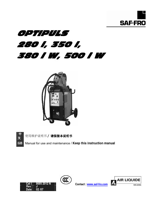
萨福铝焊机说明书
B - 安装调试 ............................................................................................................10 1. 拆除包装 .......................................................................................................10 2. 送丝机连接...................................................................................................10 3. 主电源的电路连接 .....................................................................................10 4. 焊枪的连接...................................................................................................10
中文
目录
安全说明 .....................................................................................................................2
A - 总体介绍 ...............................................................................................................7 1. 装置简介 .........................................................................................................7 2. 焊接设备组成 ................................................................................................7 3. 前面板描述.....................................................................................................8 4. 选配件..............................................................................................................8 5. OPTIPULS i / i W技术规格 .............................................................................8 6. 尺寸和重量.....................................................................................................9 7. 冷却装置的技术规格......................................................................................9
max263翻译

Max263(264)是开关电容有源滤波器设计用于精密滤波应用。
中心频率,Q,工作模式都可以通过输入引脚选择。
Max263不需要用外部元件去实现带通,低通,高通,全通滤波。
max263是专门带通应用程序和包含一个通用运算放大器。
两个第二阶滤波器部分都包含在这两个设备。
通过fclk/f0Max263和267的中心频率可以到达57KHZ,而max264和268可以到达140KHZ。
Max263(264)有28个引脚,max267(268)有24个引脚。
1、滤波器设计软件化2、中心频率32阶可控3、Q值128阶可控4、Q值与f0独立可编程5、f0可达140KHz6、支持+5V和士5V两种供电方式芯片诸引脚功能如下(括号内数字为引脚号):V+(10):供电正极, 并接旁路电容尽量靠近该脚V-(18):供电负极, 并接旁路电容尽量靠近该脚GND(19):模拟地CLKA(13):A单元元时钟输人, 该时钟在芯片内部被二分频CLKB(14):B单元时钟输人, 该时钟在芯片内部被二分频OSC OUT(20):连至晶体, 组成晶振电路(若接时钟信号时, 该脚不连)INA,INB(5,1):滤波器输人BPA,BPB(3,27): 带通输出LPA,LPB(2,28):低通输出HPA,HPB(4,26):高通、带陷、全通输出M0,M1(8,7):模式选择,+5V高,-5V低F0-F4(24,17,23,12,11):时钟与中心频率比值(FCLK/f0)编程端Q0-Q6(15,16,21,22,25,6,9):Q编程端。
1、供给电压士15V2、输入电压士0.3V3、输入电流士50Ma对M0、M1两个管脚编程可使芯片工作于模式1、2、3、4几种方式,对应的功能如表1所示。
时钟与中心频率比值与编码对应如表2所示。
模式1:当我们要实现全极点低通或带通滤波器如切比雪夫、巴特沃斯滤波器时这种模式是很有用的, 有时该模式也用来实现带陷滤波器, 但由于相关零极点位置固定, 使得用作带陷时受到限制。
- 1、下载文档前请自行甄别文档内容的完整性,平台不提供额外的编辑、内容补充、找答案等附加服务。
- 2、"仅部分预览"的文档,不可在线预览部分如存在完整性等问题,可反馈申请退款(可完整预览的文档不适用该条件!)。
- 3、如文档侵犯您的权益,请联系客服反馈,我们会尽快为您处理(人工客服工作时间:9:00-18:30)。
Package Information
MAX263/MAX264/MAX267/MAX268Pin Programmable Universal and Bandwidth Filters (The package drawing(s) in this data sheet may not reflect the most current specifications. For the latest package outline information
go to /packages.)
M A X 263/M A X 264/M A X 267/M A X 268
Pin Programmable
Universal and Bandwidth Filters 24______________________________________________________________________________________
Package Information (continued)
(The package drawing(s) in this data sheet may not reflect the most current specifications. For the latest package outline information go to /packages .)
Package Information (continued)
MAX263/MAX264/MAX267/MAX268Pin Programmable Universal and Bandwidth Filters (The package drawing(s) in this data sheet may not reflect the most current specifications. For the latest package outline information
go to /packages.)
M A X 263/M A X 264/M A X 267/M A X 268
Pin Programmable
Universal and Bandwidth Filters 26______________________________________________________________________________________
Package Information (continued)
(The package drawing(s) in this data sheet may not reflect the most current specifications. For the latest package outline information go to /packages .)
MAX263/MAX264/MAX267/MAX268
Pin Programmable
Universal and Bandwidth Filters
______________________________________________________________________________________27
Package Information (continued)
(The package drawing(s) in this data sheet may not reflect the most current specifications. For the latest package outline information go to /packages
.)
M A X 263/M A X 264/M A X 267/M A X 268
Pin Programmable
Universal and Bandwidth Filters Maxim cannot assum e responsibility for use of any circuitry other than circuitry entirely em bodied in a Maxim product. No circuit patent licenses are implied. Maxim reserves the right to change the circuitry and specifications without notice at any time.
28____________________Maxim Integrated Products, 120 San Gabriel Drive, Sunnyvale, CA 94086 408-737-7600©2008 Maxim Integrated Products
is a registered trademark of Maxim Integrated Products, Inc.。