MAX4081FAUA+T中文资料
MAX3314EEUA+T中文资料

General DescriptionThe MAX3314E is a ±5V-powered EIA/TIA-232-compat-ible interface. It has one transmitter and one receiver in a flow-through architecture. The transmitter output and the receiver input are protected to ±15kV using I EC 1000-4-2 Air-Gap Discharge, ±8kV using IEC 1000-4-2Contact Discharge, and ±15kV using the Human Body Model.The transmitter has a low-dropout output stage provid-ing minimum RS-232-compatible ±3.7V output levels while driving 3k Ωand 1000pF at 460kbps. Both +5V and -5V must be supplied externally.The MAX3314E has a SHDN function that reduces sup-ply current to 1µA. The transmitter is disabled and put into tristate while the receiver remains active.The MAX3314E is available in 8-pin µMAX, SOT23, and SO packages.________________________ApplicationsDigital CamerasPDAs GPS POSTelecommunications Handy-Terminals Set-Top BoxesFeatureso ESD Protection for RS-232 I/O Pins±15kV—Human Body Model±8kV—IEC 1000-4-2 Contact Discharge ±15kV—IEC 1000-4-2 Air-Gap Discharge o 1µA Low-Power Shutdown with Receiver Active o 30µA Operating Supply Current o 460kbps Guaranteed Data Rate o 8-Pin SOT23 Packageo ±3.7V RS-232-Compatible LevelsMAX3314E±15kV ESD-Protected, 460kbps, 1µA,RS-232-Compatible Transceiver________________________________________________________________Maxim Integrated Products 1Pin ConfigurationTypical Operating Circuit19-1696; Rev 1; 3/01Ordering InformationFor pricing, delivery, and ordering information,please contact Maxim/Dallas Direct!at 1-888-629-4642, or visit Maxim’s website at .M A X 3314E±15kV ESD-Protected, 460kbps, 1µA, RS-232-Compatible TransceiverABSOLUTE MAXIMUM RATINGSStresses beyond those listed under “Absolute Maximum Ratings” may cause permanent damage to the device. These are stress ratings only, and functional operation of the device at these or any other conditions beyond those indicated in the operational sections of the specifications is not implied. Exposure to absolute maximum rating conditions for extended periods may affect device reliability.V CC to GND.............................................................-0.3V to +6V V- to GND ...............................................................+0.3V to -6V Input VoltagesTIN, SHDN to GND...............................................-0.3V to +6V RIN to GND......................................................................±25V Output VoltagesTOUT to GND................................................................±13.2V ROUT .................................................…-0.3V to (V CC + 0.3V)Short-Circuit DurationTOUT to GND.........................................................ContinuousContinuous Power Dissipation8-Pin SOT23 (derate 9.7mW/°C above +70°C)...........777mW 8-Pin µMAX (derate 4.1mW/°C above +70°C)............300mW 8-Pin SO (derate 5.88mW/°C above +70°C)...............471mW Operating Temperature RangesMAX3314EC_A ..................................................0°C to +70°C MAX3314EE_A................................................-40°C to +85°C Junction Temperature.....................................................+150°C Storage Temperature Range............................-65°C to +150°C Lead Temperature (soldering, 10s)................................+300°CELECTRICAL CHARACTERISTICSMAX3314E±15kV ESD-Protected, 460kbps, 1µA,RS-232-Compatible Transceiver_______________________________________________________________________________________3TIMING CHARACTERISTICS021********10005001500200025003000SLEW RATE vs. LOAD CAPACITANCELOAD CAPACITANCE (pF)S L E W R A T E (V /µs)-61-1-223546010001500200025003000TRANSMITTER OUTPUT VOLTAGEvs. LOAD CAPACITANCELOAD CAPACITANCE (pF)T R A N S M I T T E R O U T P U T V O L T A G E (V )0-3-4-550000.51.01.52.02.53.03.54.04.55.05.550010001500200025003000SUPPLY CURRENT vs. LOAD CAPACITANCELOAD CAPACITANCE (pF)S U P P L Y C U R R E N T (m A )Typical Operating Characteristics(V CC = +5V, V- = -5V, 250kbps data rate, transmitter loaded with 3k Ωand C L , T A = +25°C, unless otherwise noted.)M A X 3314E±15kV ESD-Protected, 460kbps, 1µA, RS-232-Compatible Transceiver 4_______________________________________________________________________________________Detailed DescriptionRS-232-Compatible DriversThe transmitter is an inverting level translator that con-verts CMOS-logic levels to ±3.7V EIA/TIA-232-compati-ble levels. It guarantees data rates up to 460kbps with worst-case loads of 3k Ωin parallel with 1000pF. When SHDN is driven low, the transmitter is disabled and put into tristate. The transmitter input does not have a pull-up resistor. Connect to ground if unused.RS-232-Compatible ReceiversThe MAX3314E ’s receiver converts RS-232 signals to CMOS-logic output levels. The receiver is rated to receive signals to ±25V. I t will remain active during shutdown mode.MAX3314E Shutdown ModeIn shutdown mode, the transmitter output is put into high impedance (Table 1). This reduces supply current to 1µA.The time required to exit shutdown is less than 2.5µs.Applications InformationCapacitor SelectionThe capacitor type used is not critical for proper opera-tion; either polarized or nonpolarized capacitors are acceptable. I f polarized capacitors are used, connect polarity as shown in the Typical Operating Circuit . Bypass V CC and V- to ground with at least 0.1µF.Transmitter Outputs WhenExiting ShutdownFigure 1 shows the transmitter output when exiting shutdown mode. The transmitter is loaded with 3k Ωinparallel with 1000pF. The transmitter output displays no ringing or undesirable transients as the MAX3314E comes out of shutdown.High Data RatesThe MAX3314E maintains minimum RS-232-compatible ±3.7V transmitter output voltage even at high data rates.Figure 2 shows a transmitter loopback test circuit.Figure 3 shows the loopback test result at 120kbps, and Figure 4 shows the same test at 250kbps.±15kV ESD ProtectionAs with all Maxim devices, ESD-protection structures are incorporated on all pins to protect against electrostatic discharges encountered during handling and assembly.The MAX3314E driver outputs and receiver inputs have extra protection against static discharge. Maxim ’s engi-neers have developed state-of-the-art structures to pro-tect these pins against ESD of ±15kV without damage.The ESD structures withstand high ESD in all states: nor-mal operation, shutdown, and powered down. After an ESD event, Maxim ’s E versions keep working without latchup, whereas competing products can latch and must be powered down to remove latchup.ESD protection can be tested in various ways. The trans-mitter outputs and receiver inputs of the product family are characterized for protection to the following limits:•±15kV using the Human Body Model•±8kV using the Contact Discharge method specified in IEC 1000-4-2•±15kV using the IEC 1000-4-2 Air-Gap methodESD Test ConditionsESD performance depends on a variety of conditions.Contact Maxim for a reliability report that documents test setup, test methodology, and test results.Human Body ModelFigure 5 shows the Human Body Model, and Figure 6shows the current waveform it generates when dis-charged into low impedance. This model consists of a 100pF capacitor charged to the ESD voltage of interest,which is then discharged into the test device through a 1.5k Ωresistor.MAX3314E±15kV ESD-Protected, 460kbps, 1µA,RS-232-Compatible Transceiver_______________________________________________________________________________________5Figure 1. Transmitter Outputs When Exiting Shutdown or Powering Up1µs/divTIN = GNDTIN = V CCFigure 2. Loopback Test CircuitSHDN TOUTTINV CCMAX3314E V-Figure 3. Loopback Test Result at 120kbps5µs/divFigure 4. Loopback Test Result at 250kbps2µs/divM A X 3314EIEC 1000-4-2The IEC 1000-4-2 standard covers ESD testing and per-formance of finished equipment; it does not specifically refer to I Cs. The MAX3314E helps design equipment that meets Level 4 (the highest level) of I EC 1000-4-2without the need for additional ESD-protection compo-nents.The major difference between tests done using the Human Body Model and I EC 1000-4-2 is higher peak current in I EC 1000-4-2 because series resistance is lower in the IEC 1000-4-2 model. Hence, the ESD with-stand voltage measured to I EC 1000-4-2 is generally lower than that measured using the Human Body Model.Figure 7 shows the I EC 1000-4-2 model, and Figure 8shows the current waveform for the 8kV, IEC 1000-4-2,Level 4, ESD Contact Discharge test.The Air-Gap test involves approaching the device with a charged probe. The Contact Discharge method connects the probe to the device before the probe is energized.Machine ModelThe Machine Model for ESD tests all pins using a 200pF storage capacitor and zero discharge resis-tance. Its objective is to emulate the stress caused bycontact that occurs with handling and assembly during manufacturing. Of course, all pins require this protec-tion during manufacturing, not just RS-232 inputs and outputs. Therefore, after PC board assembly, the Machine Model is less relevant to I/O ports.Chip InformationTRANSISTOR COUNT: 128±15kV ESD-Protected, 460kbps, 1µA, RS-232-Compatible Transceiver 6_______________________________________________________________________________________Figure 8. IEC 1000-4-2 ESD Generator Current WaveformFigure 5. Human Body ESD Test ModelMAX3314E±15kV ESD-Protected, 460kbps, 1µA,RS-232-Compatible TransceiverPackage InformationM A X 3314E±15kV ESD-Protected, 460kbps, 1µA, RS-232-Compatible Transceiver Maxim cannot assume responsibility for use of any circuitry other than circuitry entirely embodied in a Maxim product. No circuit patent licenses are implied. Maxim reserves the right to change the circuitry and specifications without notice at any time.8_____________________Maxim Integrated Products, 120 San Gabriel Drive, Sunnyvale, CA 94086 408-737-7600©2001 Maxim Integrated ProductsPrinted USAis a registered trademark of Maxim Integrated Products.Package Information (continued)。
MAX483ESA+T中文资料
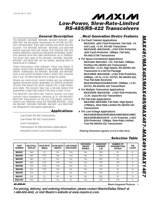
For pricing, delivery, and ordering information,please contact Maxim/Dallas Direct!at 1-888-629-4642, or visit Maxim’s website at .General DescriptionThe MAX481, MAX483, MAX485, MAX487–MAX491, and MAX1487 are low-power transceivers for RS-485 and RS-422 communication. Each part contains one driver and one receiver. The MAX483, MAX487, MAX488, and MAX489feature reduced slew-rate drivers that minimize EMI and reduce reflections caused by improperly terminated cables,thus allowing error-free data transmission up to 250kbps.The driver slew rates of the MAX481, MAX485, MAX490,MAX491, and MAX1487 are not limited, allowing them to transmit up to 2.5Mbps.These transceivers draw between 120µA and 500µA of supply current when unloaded or fully loaded with disabled drivers. Additionally, the MAX481, MAX483, and MAX487have a low-current shutdown mode in which they consume only 0.1µA. All parts operate from a single 5V supply.Drivers are short-circuit current limited and are protected against excessive power dissipation by thermal shutdown circuitry that places the driver outputs into a high-imped-ance state. The receiver input has a fail-safe feature that guarantees a logic-high output if the input is open circuit.The MAX487 and MAX1487 feature quarter-unit-load receiver input impedance, allowing up to 128 MAX487/MAX1487 transceivers on the bus. Full-duplex communi-cations are obtained using the MAX488–MAX491, while the MAX481, MAX483, MAX485, MAX487, and MAX1487are designed for half-duplex applications.________________________ApplicationsLow-Power RS-485 Transceivers Low-Power RS-422 Transceivers Level TranslatorsTransceivers for EMI-Sensitive Applications Industrial-Control Local Area Networks__Next Generation Device Features♦For Fault-Tolerant ApplicationsMAX3430: ±80V Fault-Protected, Fail-Safe, 1/4Unit Load, +3.3V, RS-485 TransceiverMAX3440E–MAX3444E: ±15kV ESD-Protected,±60V Fault-Protected, 10Mbps, Fail-Safe, RS-485/J1708 Transceivers♦For Space-Constrained ApplicationsMAX3460–MAX3464: +5V, Fail-Safe, 20Mbps,Profibus RS-485/RS-422 TransceiversMAX3362: +3.3V, High-Speed, RS-485/RS-422Transceiver in a SOT23 PackageMAX3280E–MAX3284E: ±15kV ESD-Protected,52Mbps, +3V to +5.5V, SOT23, RS-485/RS-422,True Fail-Safe ReceiversMAX3293/MAX3294/MAX3295: 20Mbps, +3.3V,SOT23, RS-855/RS-422 Transmitters ♦For Multiple Transceiver ApplicationsMAX3030E–MAX3033E: ±15kV ESD-Protected,+3.3V, Quad RS-422 Transmitters ♦For Fail-Safe ApplicationsMAX3080–MAX3089: Fail-Safe, High-Speed (10Mbps), Slew-Rate-Limited RS-485/RS-422Transceivers♦For Low-Voltage ApplicationsMAX3483E/MAX3485E/MAX3486E/MAX3488E/MAX3490E/MAX3491E: +3.3V Powered, ±15kV ESD-Protected, 12Mbps, Slew-Rate-Limited,True RS-485/RS-422 TransceiversMAX481/MAX483/MAX485/MAX487–MAX491/MAX1487Low-Power, Slew-Rate-Limited RS-485/RS-422 Transceivers______________________________________________________________Selection Table19-0122; Rev 8; 10/03Ordering Information appears at end of data sheet.M A X 481/M A X 483/M A X 485/M A X 487–M A X 491/M A X 1487Low-Power, Slew-Rate-Limited RS-485/RS-422 Transceivers 2_______________________________________________________________________________________ABSOLUTE MAXIMUM RATINGSSupply Voltage (V CC ).............................................................12V Control Input Voltage (RE , DE)...................-0.5V to (V CC + 0.5V)Driver Input Voltage (DI).............................-0.5V to (V CC + 0.5V)Driver Output Voltage (A, B)...................................-8V to +12.5V Receiver Input Voltage (A, B).................................-8V to +12.5V Receiver Output Voltage (RO).....................-0.5V to (V CC +0.5V)Continuous Power Dissipation (T A = +70°C)8-Pin Plastic DIP (derate 9.09mW/°C above +70°C)....727mW 14-Pin Plastic DIP (derate 10.00mW/°C above +70°C)..800mW 8-Pin SO (derate 5.88mW/°C above +70°C).................471mW14-Pin SO (derate 8.33mW/°C above +70°C)...............667mW 8-Pin µMAX (derate 4.1mW/°C above +70°C)..............830mW 8-Pin CERDIP (derate 8.00mW/°C above +70°C).........640mW 14-Pin CERDIP (derate 9.09mW/°C above +70°C).......727mW Operating Temperature RangesMAX4_ _C_ _/MAX1487C_ A...............................0°C to +70°C MAX4__E_ _/MAX1487E_ A.............................-40°C to +85°C MAX4__MJ_/MAX1487MJA...........................-55°C to +125°C Storage Temperature Range.............................-65°C to +160°C Lead Temperature (soldering, 10sec).............................+300°CDC ELECTRICAL CHARACTERISTICS(V CC = 5V ±5%, T A = T MIN to T MAX , unless otherwise noted.) (Notes 1, 2)Stresses beyond those listed under “Absolute Maximum Ratings” may cause permanent damage to the device. These are stress ratings only, and functional operation of the device at these or any other conditions beyond those indicated in the operational sections of the specifications is not implied. Exposure to absolute maximum rating conditions for extended periods may affect device reliability.V V IN = -7VV IN = 12V V IN = -7V V IN = 12V Input Current (A, B)I IN2V TH k Ω48-7V ≤V CM ≤12V, MAX487/MAX1487R INReceiver Input Resistance -7V ≤V CM ≤12V, all devices except MAX487/MAX1487R = 27Ω(RS-485), Figure 40.4V ≤V O ≤2.4VR = 50Ω(RS-422)I O = 4mA, V ID = -200mV I O = -4mA, V ID = 200mV V CM = 0V-7V ≤V CM ≤12V DE, DI, RE DE, DI, RE MAX487/MAX1487,DE = 0V, V CC = 0V or 5.25VDE, DI, RE R = 27Ωor 50Ω, Figure 4R = 27Ωor 50Ω, Figure 4R = 27Ωor 50Ω, Figure 4DE = 0V;V CC = 0V or 5.25V,all devices except MAX487/MAX1487CONDITIONSk Ω12µA ±1I OZRThree-State (high impedance)Output Current at ReceiverV 0.4V OL Receiver Output Low Voltage 3.5V OH Receiver Output High Voltage mV 70∆V TH Receiver Input Hysteresis V -0.20.2Receiver Differential Threshold Voltage-0.2mA 0.25mA-0.81.01.55V OD2Differential Driver Output (with load)V 2V 5V OD1Differential Driver Output (no load)µA±2I IN1Input CurrentV 0.8V IL Input Low Voltage V 2.0V IH Input High Voltage V 0.2∆V OD Change in Magnitude of Driver Common-Mode Output Voltage for Complementary Output States V 0.2∆V OD Change in Magnitude of Driver Differential Output Voltage for Complementary Output States V 3V OC Driver Common-Mode Output VoltageUNITS MINTYPMAX SYMBOL PARAMETERMAX481/MAX483/MAX485/MAX487–MAX491/MAX1487Low-Power, Slew-Rate-Limited RS-485/RS-422 Transceivers_______________________________________________________________________________________3SWITCHING CHARACTERISTICS—MAX481/MAX485, MAX490/MAX491, MAX1487(V CC = 5V ±5%, T A = T MIN to T MAX , unless otherwise noted.) (Notes 1, 2)DC ELECTRICAL CHARACTERISTICS (continued)(V CC = 5V ±5%, T A = T MIN to T MAX , unless otherwise noted.) (Notes 1, 2)ns 103060t PHLDriver Rise or Fall Time Figures 6 and 8, R DIFF = 54Ω, C L1= C L2= 100pF ns MAX490M, MAX491M MAX490C/E, MAX491C/E2090150MAX481, MAX485, MAX1487MAX490M, MAX491MMAX490C/E, MAX491C/E MAX481, MAX485, MAX1487Figures 6 and 8, R DIFF = 54Ω,C L1= C L2= 100pF MAX481 (Note 5)Figures 5 and 11, C RL = 15pF, S2 closedFigures 5 and 11, C RL = 15pF, S1 closed Figures 5 and 11, C RL = 15pF, S2 closed Figures 5 and 11, C RL = 15pF, S1 closed Figures 6 and 10, R DIFF = 54Ω,C L1= C L2= 100pFFigures 6 and 8,R DIFF = 54Ω,C L1= C L2= 100pF Figures 6 and 10,R DIFF = 54Ω,C L1= C L2= 100pF CONDITIONS ns 510t SKEW ns50200600t SHDNTime to ShutdownMbps 2.5f MAX Maximum Data Rate ns 2050t HZ Receiver Disable Time from High ns 103060t PLH 2050t LZ Receiver Disable Time from Low ns 2050t ZH Driver Input to Output Receiver Enable to Output High ns 2050t ZL Receiver Enable to Output Low 2090200ns ns 134070t HZ t SKD Driver Disable Time from High |t PLH - t PHL |DifferentialReceiver Skewns 4070t LZ Driver Disable Time from Low ns 4070t ZL Driver Enable to Output Low 31540ns51525ns 31540t R , t F 2090200Driver Output Skew to Output t PLH , t PHL Receiver Input to Output4070t ZH Driver Enable to Output High UNITS MIN TYP MAX SYMBOL PARAMETERFigures 7 and 9, C L = 100pF, S2 closed Figures 7 and 9, C L = 100pF, S1 closed Figures 7 and 9, C L = 15pF, S1 closed Figures 7 and 9, C L = 15pF, S2 closedM A X 481/M A X 483/M A X 485/M A X 487–M A X 491/M A X 1487Low-Power, Slew-Rate-Limited RS-485/RS-422 Transceivers 4_______________________________________________________________________________________SWITCHING CHARACTERISTICS—MAX483, MAX487/MAX488/MAX489(V CC = 5V ±5%, T A = T MIN to T MAX , unless otherwise noted.) (Notes 1, 2)SWITCHING CHARACTERISTICS—MAX481/MAX485, MAX490/MAX491, MAX1487 (continued)(V CC = 5V ±5%, T A = T MIN to T MAX , unless otherwise noted.) (Notes 1, 2)3001000Figures 7 and 9, C L = 100pF, S2 closed Figures 7 and 9, C L = 100pF, S1 closed Figures 5 and 11, C L = 15pF, S2 closed,A - B = 2VCONDITIONSns 40100t ZH(SHDN)Driver Enable from Shutdown toOutput High (MAX481)nsFigures 5 and 11, C L = 15pF, S1 closed,B - A = 2Vt ZL(SHDN)Receiver Enable from Shutdownto Output Low (MAX481)ns 40100t ZL(SHDN)Driver Enable from Shutdown toOutput Low (MAX481)ns 3001000t ZH(SHDN)Receiver Enable from Shutdownto Output High (MAX481)UNITS MINTYP MAX SYMBOLPARAMETERt PLH t SKEW Figures 6 and 8, R DIFF = 54Ω,C L1= C L2= 100pFt PHL Figures 6 and 8, R DIFF = 54Ω,C L1= C L2= 100pFDriver Input to Output Driver Output Skew to Output ns 100800ns ns 2000MAX483/MAX487, Figures 7 and 9,C L = 100pF, S2 closedt ZH(SHDN)Driver Enable from Shutdown to Output High2502000ns2500MAX483/MAX487, Figures 5 and 11,C L = 15pF, S1 closedt ZL(SHDN)Receiver Enable from Shutdown to Output Lowns 2500MAX483/MAX487, Figures 5 and 11,C L = 15pF, S2 closedt ZH(SHDN)Receiver Enable from Shutdown to Output Highns 2000MAX483/MAX487, Figures 7 and 9,C L = 100pF, S1 closedt ZL(SHDN)Driver Enable from Shutdown to Output Lowns 50200600MAX483/MAX487 (Note 5) t SHDN Time to Shutdownt PHL t PLH , t PHL < 50% of data period Figures 5 and 11, C RL = 15pF, S2 closed Figures 5 and 11, C RL = 15pF, S1 closed Figures 5 and 11, C RL = 15pF, S2 closed Figures 5 and 11, C RL = 15pF, S1 closed Figures 7 and 9, C L = 15pF, S2 closed Figures 6 and 10, R DIFF = 54Ω,C L1= C L2= 100pFFigures 7 and 9, C L = 15pF, S1 closed Figures 7 and 9, C L = 100pF, S1 closed Figures 7 and 9, C L = 100pF, S2 closed CONDITIONSkbps 250f MAX 2508002000Maximum Data Rate ns 2050t HZ Receiver Disable Time from High ns 25080020002050t LZ Receiver Disable Time from Low ns 2050t ZH Receiver Enable to Output High ns 2050t ZL Receiver Enable to Output Low ns ns 1003003000t HZ t SKD Driver Disable Time from High I t PLH - t PHL I DifferentialReceiver SkewFigures 6 and 10, R DIFF = 54Ω,C L1= C L2= 100pFns 3003000t LZ Driver Disable Time from Low ns 2502000t ZL Driver Enable to Output Low ns Figures 6 and 8, R DIFF = 54Ω,C L1= C L2= 100pFns 2502000t R , t F 2502000Driver Rise or Fall Time ns t PLH Receiver Input to Output2502000t ZH Driver Enable to Output High UNITS MIN TYP MAX SYMBOL PARAMETERMAX481/MAX483/MAX485/MAX487–MAX491/MAX1487Low-Power, Slew-Rate-Limited RS-485/RS-422 Transceivers_______________________________________________________________________________________530002.5OUTPUT CURRENT vs.RECEIVER OUTPUT LOW VOLTAGE525M A X 481-01OUTPUT LOW VOLTAGE (V)O U T P U T C U R R E N T (m A )1.515100.51.02.0203540450.90.1-50-252575RECEIVER OUTPUT LOW VOLTAGE vs.TEMPERATURE0.30.7TEMPERATURE (°C)O U T P U TL O W V O L T A G E (V )500.50.80.20.60.40100125-20-41.5 2.0 3.0 5.0OUTPUT CURRENT vs.RECEIVER OUTPUT HIGH VOLTAGE-8-16M A X 481-02OUTPUT HIGH VOLTAGE (V)O U T P U T C U R R E N T (m A )2.5 4.0-12-18-6-14-10-203.54.5 4.83.2-50-252575RECEIVER OUTPUT HIGH VOLTAGE vs.TEMPERATURE3.64.4TEMPERATURE (°C)O U T P UT H I G H V O L T A G E (V )0504.04.63.44.23.83.01001259000 1.0 3.0 4.5DRIVER OUTPUT CURRENT vs.DIFFERENTIAL OUTPUT VOLTAGE1070M A X 481-05DIFFERENTIAL OUTPUT VOLTAGE (V)O U T P U T C U R R E N T (m A )2.0 4.05030806040200.5 1.5 2.53.5 2.31.5-50-2525125DRIVER DIFFERENTIAL OUTPUT VOLTAGEvs. TEMPERATURE1.72.1TEMPERATURE (°C)D I F FE R E N T I A L O U T P U T V O L T A G E (V )751.92.21.62.01.8100502.4__________________________________________Typical Operating Characteristics(V CC = 5V, T A = +25°C, unless otherwise noted.)NOTES FOR ELECTRICAL/SWITCHING CHARACTERISTICSNote 1:All currents into device pins are positive; all currents out of device pins are negative. All voltages are referenced to deviceground unless otherwise specified.Note 2:All typical specifications are given for V CC = 5V and T A = +25°C.Note 3:Supply current specification is valid for loaded transmitters when DE = 0V.Note 4:Applies to peak current. See Typical Operating Characteristics.Note 5:The MAX481/MAX483/MAX487 are put into shutdown by bringing RE high and DE low. If the inputs are in this state for lessthan 50ns, the parts are guaranteed not to enter shutdown. If the inputs are in this state for at least 600ns, the parts are guaranteed to have entered shutdown. See Low-Power Shutdown Mode section.M A X 481/M A X 483/M A X 485/M A X 487–M A X 491/M A X 1487Low-Power, Slew-Rate-Limited RS-485/RS-422 Transceivers 6___________________________________________________________________________________________________________________Typical Operating Characteristics (continued)(V CC = 5V, T A = +25°C, unless otherwise noted.)120008OUTPUT CURRENT vs.DRIVER OUTPUT LOW VOLTAGE20100M A X 481-07OUTPUT LOW VOLTAGE (V)O U T P U T C U R R E N T (m A )6604024801012140-1200-7-5-15OUTPUT CURRENT vs.DRIVER OUTPUT HIGH VOLTAGE-20-80M A X 481-08OUTPUT HIGH VOLTAGE (V)O U T P U T C U R R E N T (m A )-31-603-6-4-2024-100-40100-40-60-2040100120MAX1487SUPPLY CURRENT vs. TEMPERATURE300TEMPERATURE (°C)S U P P L Y C U R R E N T (µA )20608050020060040000140100-50-2550100MAX481/MAX485/MAX490/MAX491SUPPLY CURRENT vs. TEMPERATURE300TEMPERATURE (°C)S U P P L Y C U R R E N T (µA )257550020060040000125100-50-2550100MAX483/MAX487–MAX489SUPPLY CURRENT vs. TEMPERATURE300TEMPERATURE (°C)S U P P L Y C U R R E N T (µA )257550020060040000125MAX481/MAX483/MAX485/MAX487–MAX491/MAX1487Low-Power, Slew-Rate-Limited RS-485/RS-422 Transceivers_______________________________________________________________________________________7______________________________________________________________Pin DescriptionFigure 1. MAX481/MAX483/MAX485/MAX487/MAX1487 Pin Configuration and Typical Operating CircuitM A X 481/M A X 483/M A X 485/M A X 487–M A X 491/M A X 1487__________Applications InformationThe MAX481/MAX483/MAX485/MAX487–MAX491 and MAX1487 are low-power transceivers for RS-485 and RS-422 communications. The MAX481, MAX485, MAX490,MAX491, and MAX1487 can transmit and receive at data rates up to 2.5Mbps, while the MAX483, MAX487,MAX488, and MAX489 are specified for data rates up to 250kbps. The MAX488–MAX491 are full-duplex trans-ceivers while the MAX481, MAX483, MAX485, MAX487,and MAX1487 are half-duplex. In addition, Driver Enable (DE) and Receiver Enable (RE) pins are included on the MAX481, MAX483, MAX485, MAX487, MAX489,MAX491, and MAX1487. When disabled, the driver and receiver outputs are high impedance.MAX487/MAX1487:128 Transceivers on the BusThe 48k Ω, 1/4-unit-load receiver input impedance of the MAX487 and MAX1487 allows up to 128 transceivers on a bus, compared to the 1-unit load (12k Ωinput impedance) of standard RS-485 drivers (32 trans-ceivers maximum). Any combination of MAX487/MAX1487 and other RS-485 transceivers with a total of 32 unit loads or less can be put on the bus. The MAX481/MAX483/MAX485 and MAX488–MAX491 have standard 12k ΩReceiver Input impedance.Low-Power, Slew-Rate-Limited RS-485/RS-422 Transceivers 8_______________________________________________________________________________________Figure 2. MAX488/MAX490 Pin Configuration and Typical Operating CircuitFigure 3. MAX489/MAX491 Pin Configuration and Typical Operating CircuitMAX483/MAX487/MAX488/MAX489:Reduced EMI and ReflectionsThe MAX483 and MAX487–MAX489 are slew-rate limit-ed, minimizing EMI and reducing reflections caused by improperly terminated cables. Figure 12 shows the dri-ver output waveform and its Fourier analysis of a 150kHz signal transmitted by a MAX481, MAX485,MAX490, MAX491, or MAX1487. High-frequency har-monics with large amplitudes are evident. Figure 13shows the same information displayed for a MAX483,MAX487, MAX488, or MAX489 transmitting under the same conditions. Figure 13’s high-frequency harmonics have much lower amplitudes, and the potential for EMI is significantly reduced.MAX481/MAX483/MAX485/MAX487–MAX491/MAX1487Low-Power, Slew-Rate-Limited RS-485/RS-422 Transceivers_______________________________________________________________________________________9_________________________________________________________________Test CircuitsFigure 4. Driver DC Test Load Figure 5. Receiver Timing Test LoadFigure 6. Driver/Receiver Timing Test Circuit Figure 7. Driver Timing Test LoadM A X 481/M A X 483/M A X 485/M A X 487–M A X 491/M A X 1487Low-Power, Slew-Rate-Limited RS-485/RS-422 Transceivers 10_______________________________________________________Switching Waveforms_________________Function Tables (MAX481/MAX483/MAX485/MAX487/MAX1487)Figure 8. Driver Propagation DelaysFigure 9. Driver Enable and Disable Times (except MAX488 and MAX490)Figure 10. Receiver Propagation DelaysFigure 11. Receiver Enable and Disable Times (except MAX488and MAX490)Table 1. TransmittingTable 2. ReceivingLow-Power Shutdown Mode (MAX481/MAX483/MAX487)A low-power shutdown mode is initiated by bringing both RE high and DE low. The devices will not shut down unless both the driver and receiver are disabled.In shutdown, the devices typically draw only 0.1µA of supply current.RE and DE may be driven simultaneously; the parts are guaranteed not to enter shutdown if RE is high and DE is low for less than 50ns. If the inputs are in this state for at least 600ns, the parts are guaranteed to enter shutdown.For the MAX481, MAX483, and MAX487, the t ZH and t ZL enable times assume the part was not in the low-power shutdown state (the MAX485/MAX488–MAX491and MAX1487 can not be shut down). The t ZH(SHDN)and t ZL(SHDN)enable times assume the parts were shut down (see Electrical Characteristics ).It takes the drivers and receivers longer to become enabled from the low-power shutdown state (t ZH(SHDN ), t ZL(SHDN)) than from the operating mode (t ZH , t ZL ). (The parts are in operating mode if the –R —E –,DE inputs equal a logical 0,1 or 1,1 or 0, 0.)Driver Output ProtectionExcessive output current and power dissipation caused by faults or by bus contention are prevented by two mechanisms. A foldback current limit on the output stage provides immediate protection against short cir-cuits over the whole common-mode voltage range (see Typical Operating Characteristics ). In addition, a ther-mal shutdown circuit forces the driver outputs into a high-impedance state if the die temperature rises excessively.Propagation DelayMany digital encoding schemes depend on the differ-ence between the driver and receiver propagation delay times. Typical propagation delays are shown in Figures 15–18 using Figure 14’s test circuit.The difference in receiver delay times, | t PLH - t PHL |, is typically under 13ns for the MAX481, MAX485,MAX490, MAX491, and MAX1487 and is typically less than 100ns for the MAX483 and MAX487–MAX489.The driver skew times are typically 5ns (10ns max) for the MAX481, MAX485, MAX490, MAX491, and MAX1487, and are typically 100ns (800ns max) for the MAX483 and MAX487–MAX489.MAX481/MAX483/MAX485/MAX487–MAX491/MAX1487Low-Power, Slew-Rate-Limited RS-485/RS-422 Transceivers______________________________________________________________________________________1110dB/div0Hz5MHz500kHz/div10dB/div0Hz5MHz500kHz/divFigure 12. Driver Output Waveform and FFT Plot of MAX481/MAX485/MAX490/MAX491/MAX1487 Transmitting a 150kHz SignalFigure 13. Driver Output Waveform and FFT Plot of MAX483/MAX487–MAX489 Transmitting a 150kHz SignalM A X 481/M A X 483/M A X 485/M A X 487–M A X 491/M A X 1487Low-Power, Slew-Rate-Limited RS-485/RS-422 Transceivers 12______________________________________________________________________________________V CC = 5V T A = +25°CV CC = 5V T A = +25°CV CC = 5V T A = +25°CV CC = 5V T A = +25°CFigure 14. Receiver Propagation Delay Test CircuitFigure 15. MAX481/MAX485/MAX490/MAX491/MAX1487Receiver t PHLFigure 16. MAX481/MAX485/MAX490/MAX491/MAX1487Receiver t PLHPHL Figure 18. MAX483, MAX487–MAX489 Receiver t PLHLine Length vs. Data RateThe RS-485/RS-422 standard covers line lengths up to 4000 feet. For line lengths greater than 4000 feet, see Figure 23.Figures 19 and 20 show the system differential voltage for the parts driving 4000 feet of 26AWG twisted-pair wire at 110kHz into 120Ωloads.Typical ApplicationsThe MAX481, MAX483, MAX485, MAX487–MAX491, and MAX1487 transceivers are designed for bidirectional data communications on multipoint bus transmission lines.Figures 21 and 22 show typical network applications circuits. These parts can also be used as line repeaters, with cable lengths longer than 4000 feet, as shown in Figure 23.To minimize reflections, the line should be terminated at both ends in its characteristic impedance, and stub lengths off the main line should be kept as short as possi-ble. The slew-rate-limited MAX483 and MAX487–MAX489are more tolerant of imperfect termination.MAX481/MAX483/MAX485/MAX487–MAX491/MAX1487Low-Power, Slew-Rate-Limited RS-485/RS-422 Transceivers______________________________________________________________________________________13DIV Y -V ZRO5V 0V1V0V -1V5V 0V2µs/divFigure 19. MAX481/MAX485/MAX490/MAX491/MAX1487 System Differential Voltage at 110kHz Driving 4000ft of Cable Figure 20. MAX483, MAX487–MAX489 System Differential Voltage at 110kHz Driving 4000ft of CableFigure 21. MAX481/MAX483/MAX485/MAX487/MAX1487 Typical Half-Duplex RS-485 NetworkM A X 481/M A X 483/M A X 485/M A X 487–M A X 491/M A X 1487Low-Power, Slew-Rate-Limited RS-485/RS-422 Transceivers 14______________________________________________________________________________________Figure 22. MAX488–MAX491 Full-Duplex RS-485 NetworkFigure 23. Line Repeater for MAX488–MAX491Isolated RS-485For isolated RS-485 applications, see the MAX253 and MAX1480 data sheets.MAX481/MAX483/MAX485/MAX487–MAX491/MAX1487Low-Power, Slew-Rate-Limited RS-485/RS-422 Transceivers______________________________________________________________________________________15_______________Ordering Information_________________Chip TopographiesMAX481/MAX483/MAX485/MAX487/MAX1487N.C. RO 0.054"(1.372mm)0.080"(2.032mm)DE DIGND B N.C.V CCARE * Contact factory for dice specifications.__Ordering Information (continued)M A X 481/M A X 483/M A X 485/M A X 487–M A X 491/M A X 1487Low-Power, Slew-Rate-Limited RS-485/RS-422 Transceivers 16______________________________________________________________________________________TRANSISTOR COUNT: 248SUBSTRATE CONNECTED TO GNDMAX488/MAX490B RO 0.054"(1.372mm)0.080"(2.032mm)N.C. DIGND Z A V CCYN.C._____________________________________________Chip Topographies (continued)MAX489/MAX491B RO 0.054"(1.372mm)0.080"(2.032mm)DE DIGND Z A V CCYREMAX481/MAX483/MAX485/MAX487–MAX491/MAX1487Low-Power, Slew-Rate-Limited RS-485/RS-422 Transceivers______________________________________________________________________________________17Package Information(The package drawing(s) in this data sheet may not reflect the most current specifications. For the latest package outline information go to /packages .)S O I C N .E P SM A X 481/M A X 483/M A X 485/M A X 487–M A X 491/M A X 1487Low-Power, Slew-Rate-Limited RS-485/RS-422 Transceivers 18______________________________________________________________________________________Package Information (continued)(The package drawing(s) in this data sheet may not reflect the most current specifications. For the latest package outline information go to /packages .)MAX481/MAX483/MAX485/MAX487–MAX491Low-Power, Slew-Rate-Limited RS-485/RS-422 TransceiversMaxim cannot assume responsibility for use of any circuitry other than circuitry entirely embodied in a Maxim product. No circuit patent licenses are implied. Maxim reserves the right to change the circuitry and specifications without notice at any time.Maxim Integrated Products, 120 San Gabriel Drive, Sunnyvale, CA 94086 408-737-7600 ____________________19©2003 Maxim Integrated ProductsPrinted USAis a registered trademark of Maxim Integrated Products.M A X 481/M A X 483/M A X 485/M A X 487–M A X 491/M A X 1487P D I P N .E PSPackage Information (continued)(The package drawing(s) in this data sheet may not reflect the most current specifications. For the latest package outline information go to /packages .)。
MAX3280EAUK+T中文资料

Features
o ESD Protection: ±15kV–Human Body Model ±6kV–IEC 1000-4-2, Contact Discharge ±12kV–IEC 1000-4-2, Air-Gap Discharge
o Guaranteed 52Mbps Data Rate o Guaranteed 15ns Receiver Propagation Delay o Guaranteed 2ns Receiver Skew o Guaranteed 8ns Package-to-Package Skew Time o VL Pin for Connection to FPGAs/ASICs o Allow Up to 128 Transceivers on the Bus
Receiver Output Voltage (RO)....................-0.3V to (VCC + 0.3V) Receiver Output Voltage
(RO) (MAX3284E) .....................................-0.3V to (VL + 0.3V) Receiver Output Short-Circuit Current .......................Continuous
ENABLE —
Active High Active Low
—
DATA RATE 52Mbps 52Mbps 52Mbps
52Mbps (Note 1)
PACKAGE 5-Pin SOT23 6-Pin SOT23 6-Pin SOT23 6-Pin SOT23
________________________________________________________________ Maxim Integrated Products 1
MAX4080TASA+中文资料
The MAX4080/MAX4081 operate from a 4.5V to 76V single supply and draw only 75µA of supply current. These devices are specified over the automotive operating temperature range (-40°C to +125°C) and are available in a space-saving 8-pin µMAX or SO package.
Operating Temperature Range .........................-40°C to +125°C Junction Temperature ......................................................+150°C Storage Temperature Range .............................-65°C to +150°C Lead Temperature (soldering, 10s) .................................+300°C
MAX485中文数据手册资料
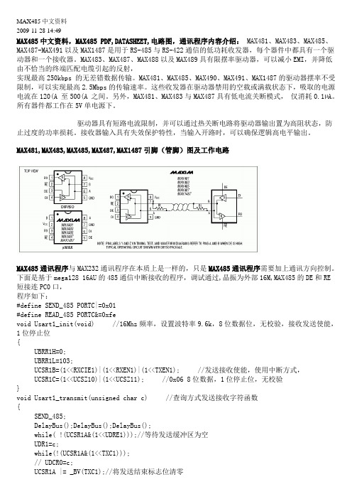
MAX485中文资料2009-11-28 14:49MAX485中文资料,MAX485 PDF,DATASHEET,电路图,通讯程序内容介绍:MAX481、MAX483、MAX485、MAX487-MAX491以及MAX1487是用于RS-485与RS-422通信的低功耗收发器,每个器件中都具有一个驱动器和一个接收器。
MAX483、MAX487、MAX488以及MAX489具有限摆率驱动器,可以减小EMI,并降低由不恰当的终端匹配电缆引起的反射,实现最高250kbps 的无差错数据传输。
MAX481、MAX485、MAX490、MAX491、MAX1487的驱动器摆率不受限制,可以实现最高2.5Mbps的传输速率。
这些收发器在驱动器禁用的空载或满载状态下,吸取的电源电流在120(A 至500(A 之间。
另外,MAX481、MAX483与MAX487具有低电流关断模式,仅消耗0.1µA。
所有器件都工作在5V单电源下。
驱动器具有短路电流限制,并可以通过热关断电路将驱动器输出置为高阻状态,防止过度的功率损耗。
接收器输入具有失效保护特性,当输入开路时,可以确保逻辑高电平输出。
MAX481,MAX483,MAX485,MAX487,MAX1487引脚(管脚)图及工作电路MAX485通讯程序与MAX232通讯程序在本质上是一样的,只是MAX485通讯程序需要加上通讯方向控制。
下面是基于mega128 16AU的485通信中断接收的程序,调试通过,晶振为外部16M,MAX485的DE和RE短接连PC0口,程序如下:#define SEND_485 PORTC|=0x01#define READ_485 PORTC&=0xfevoid Usart1_init(void) //16Mhz频率,设置波特率9.6k,8位数据位,无校验,接收发送使能,1位停止位{UBRR1H=0;UBRR1L=103;UCSR1B=(1<<RXCIE1)|(1<<RXEN1)|(1<<TXEN1); //发送接收使能,使用中断方式,UCSR1C=(1<<UCSZ10)|(1<<UCSZ11); //0x06 8位数据,1位停止位,无校验}void Usart1_transmit(unsigned char c) //查询方式发送接收字符函数{SEND_485;DelayBus();DelayBus();DelayBus();while( !(UCSR1A&(1<<UDRE1)));//等待发送缓冲区为空UDR1=c;while(!(UCSR1A&(1<<TXC1)));// UDCR0=c;UCSR1A |= _BV(TXC1);//将发送结束标志位清零// SET_BIT(UCSR1A,);READ_485;direction++;}SIGNAL(SIG_UART1_RECV)//serial port 1 {if(UCSR1A&(1<<RXC1)){rec1buff=UDR1;rec1_flag=1;。
MAX4060EUA中文资料

ELECTRICAL CHARACTERISTICS
(VCC = 3V for MAX4061/MAX4062, VCC = 5V for MAX4060, GND = 0V, SHDN = VCC, INT/AUX = 0V, RG = 11.11kΩ, RL = 100kΩ to 1.5V, RBIAS = ∞, TA = TMIN to TMAX, unless otherwise noted. Typical values are at TA = +25°C.) (Notes 1, 2)
TEMP RANGE
MAX4060ETA -40°C to +85°C
MAX4060EUA -40°C to +85°C
MAX4061ETA -40°C to +85°C
MAX4061EUA -40°C to +85°C
MAX4062EUB -40°C to +85°C
*EP = Exposed paddle.
Input Noise-Voltage Density
BW-3dB RIN
RMATCH
en
Either differential input
AV = 10V/V, f = 1kHz AV = 100V/V, f = 1kHz, MAX4061/MAX4062 only
RMS Output Noise Voltage
元1/03
MAX4060/MAX4061/MAX4062
Differential Microphone Preamplifiers with Internal Bias and Complete Shutdown
General Description
MAX5095AAUA-T中文资料

General DescriptionThe MAX5094A/B/C/D/MAX5095A/B/C BiCMOS, high-performance, current-mode PWM controllers have all the features required for wide input-voltage range isolated/nonisolated power supplies. These controllers are used for low- and high-power universal input volt-age and telecom power supplies.The MAX5094/MAX5095 contain a fast comparator with only 60ns typical delay from current sense to the output for overcurrent protection. The MAX5094 has an inte-grated error amplifier with the output at COMP. Soft-start is achieved by controlling the COMP voltage rise using external components.The oscillator frequency is adjustable from 20kH z to 1MHz with an external resistor and capacitor. The tim-ing capacitor discharge current is trimmed allowing for programmable dead time and maximum duty cycle for a given frequency. The available saw-toothed waveform at R T C T can be used for slope compensation when needed.The MAX5095A/MAX5095B include a bidirectional syn-chronization circuit allowing for multiple controllers to run at the same frequency to avoid beat frequencies.Synchronization is accomplished by simply connecting the SYNC of all devices together. When synchronizing with other devices, the MAX5095A/MAX5095B with the highest frequency synchronizes the other devices.Alternatively, the MAX5095A/MAX5095B can be syn-chronized to an external clock with an open-drain out-put stage running at a higher frequency.The MAX5095C provides a clock output pulse (ADV_CLK) that leads the driver output (OUT) by 110ns. The advanced clock signal is used to drive the secondary-side synchronous rectifiers.The MAX5094A/B/C are available in the 8-pin SO and 8-pin µMAX ®packages. The MAX5094D and MAX5095A/B/C are available in the 8-pin µMAX pack-age. All devices operate over the automotive tempera-ture range of -40°C to +125°C.ApplicationsUniversal Input AC/DC Power Supplies Isolated Telecom Power Supplies Isolated Power-Supply Modules Networking SystemsComputer Systems/Servers Industrial Power Conversion Isolated Keep-Alive CircuitsFeatures♦Pin-for-Pin Replacement for UCC28C43(MAX5094A) and UCC28C45 (MAX5094B)♦2A Drive Source and 1A Sink Capability ♦Up to 1MHz Switching Frequency Operation ♦Bidirectional Frequency Synchronization (MAX5095A/MAX5095B)♦Advanced Output Drive for Secondary-Side Synchronous Rectification (MAX5095C)♦Fast 60ns Cycle-by-Cycle Current Limit♦Trimmed Oscillator Capacitor Discharge Current Sets Maximum Duty Cycle Accurately ♦Accurate ±5% Start Voltage with 0.8V Hysteresis ♦Low 32µA Startup Current♦5V Regulator Output (REF) with 20mA Capability ♦Versions with 0.3V Current-Sense Threshold ♦Overtemperature ShutdownMAX5094A/B/C/D/MAX5095A/B/CHigh-Performance, Single-Ended, Current-ModePWM Controllers________________________________________________________________Maxim Integrated Products119-3864; Rev 3; 10/06For pricing, delivery, and ordering information,please contact Maxim/Dallas Direct!at 1-888-629-4642, or visit Maxim’s website at .µMAX is a registered trademark of Maxim Integrated Products, Inc.M A X 5094A /B /C /D /M A X 5095A /B /CPWM ControllersABSOLUTE MAXIMUM RATINGSELECTRICAL CHARACTERISTICSStresses beyond those listed under “Absolute Maximum Ratings” may cause permanent damage to the device. These are stress ratings only, and functional operation of the device at these or any other conditions beyond those indicated in the operational sections of the specifications is not implied. Exposure to absolute maximum rating conditions for extended periods may affect device reliability.V CC (Low-Impedance Source) to GND..................-0.3V to +30V V CC (I CC < 30mA).....................................................Self Limiting OUT to GND...............................................-0.3V to (V CC + 0.3V)OUT Current.............................................................±1A for 10µs FB, SYNC, COMP, CS, R T /C T , REF to GND.............-0.3V to +6V COMP Sink Current (MAX5094)..........................................10mAContinuous Power Dissipation (T A = +70°C)8-Pin µMAX (derate 4.5mW/°C above +70°C).............362mW 8-Pin SO (derate 5.9mW/°C above +70°C)...............470.6mW Operating Temperature Range .........................-40°C to +125°C Maximum Junction Temperature.....................................+150°C Storage Temperature Range.............................-65°C to +150°C Lead Temperature (soldering, 10s).................................+300°CELECTRICAL CHARACTERISTICS (continued)MAX5094A/B/C/D/MAX5095A/B/C PWM Controllers(V= +15V, R= 10kΩ, C= 3.3nF, REF = open, C= 0.1µF, COMP = open, V= 2V, CS = GND, T= T= -40°C to +85°C,M A X 5094A /B /C /D /M A X 5095A /B /CPWM ControllersELECTRICAL CHARACTERISTICS (continued)(V CC = +15V, R T = 10k Ω, C T = 3.3nF, REF = open, C REF = 0.1µF, COMP = open, V FB = 2V, CS = GND, T A = T J = -40°C to +85°C ,unless otherwise noted.) (Note 1)ELECTRICAL CHARACTERISTICS(V = +15V, R = 10k Ω, C = 3.3nF, REF = open, C = 0.1µF, COMP = open, V = 2V, CS = GND, T = T = -40°C to +125°C ,ELECTRICAL CHARACTERISTICS (continued)MAX5094A/B/C/D/MAX5095A/B/C PWM Controllers(V= +15V, R= 10kΩ, C= 3.3nF, REF = open, C= 0.1µF, COMP = open, V= 2V, CS = GND, T= T= -40°C to +125°C,M A X 5094A /B /C /D /M A X 5095A /B /CPWM Controllers 6_______________________________________________________________________________________ELECTRICAL CHARACTERISTICS (continued)Note 1:All devices are 100% tested at +25°C. All limits over temperature are guaranteed by design, not production tested.Note 2:Guaranteed by design, not production tested.Note 3:Parameter measured at trip point of latch with V FB = 0 (MAX5094 only).Note 4:Gain is defined as A = ∆V COMP / ∆V CS , 0 ≤V CS ≤0.8V for MAX5094A/MAX5094B, 0 ≤V CS ≤0.2V for MAX5094C/MAX5094D/ MAX5095_.Note 5:Output frequency equals oscillator frequency for MAX5094A/MAX5094C/MAX5095A. Output frequency is one-half oscillatorfrequency for MAX5094B/MAX5094D/MAX5095B/MAX5095C.Typical Operating Characteristics(V CC = 15V, T A = +25°C, unless otherwise noted.)BOOTSTRAP UVLO vs. TEMPERATURETEMPERATURE (°C)V C C (V )110956580-105203550-25012345678910-40125252739312933353741-40-10520-253550958011065125STARTUP CURRENT vs. TEMPERATURETEMPERATURE (°C)I C C (µA )3.53.74.94.13.94.34.54.75.1OPERATING SUPPLY CURRENT vs. TEMPERATURE AFTER STARTUP(f OSC = f SW = 300kHz)I C C (m A )-40-10520-253550958011065125TEMPERATURE (°C)MAX5094A/B/C/D/MAX5095A/B/CPWM Controllers_______________________________________________________________________________________7Typical Operating Characteristics (continued)(V CC = 15V, T A = +25°C, unless otherwise noted.)4.904.944.925.004.984.965.025.045.065.08REFERENCE VOLTAGE vs. TEMPERATUREV R E F (V )-40-10520-253550958011065125TEMPERATURE (°C)4.654.754.704.854.805.004.954.905.05020103040506070REFERENCE VOLTAGE vs. REFERENCE LOAD CURRENTM A X 5094/95 t o c 05I REF (mA)V R E F (V ) 4.9804.9844.9824.9884.9864.9924.9904.9944.9984.9965.000101416121820222426REFERENCE VOLTAGE vs. SUPPLY VOLTAGEV CC (V)V R E F (V )450470460500490480510520540530550-40-105-25203550658095110125OSCILLATOR FREQUENCY (f OSC )vs. TEMPERATURETEMPERATURE (°C)O S C I L L A T O R F R E Q U E N C Y (k H z )7.887.908.027.947.927.967.988.008.04-40-10520-253550958011065125OSCILLATOR R T /C TDISCHARGE CURRENTvs. TEMPERATURETEMPERATURE (°C)R T /C T D I S C H A R G E C U R R E N T (m A )201050403060709080100MAXIMUM DUTY CYCLE vs. TEMPERATURED U T Y C Y C LE (%)-40-10520-253550958011065125TEMPERATURE (°C)1000150050020002500300035004000MAXIMUM DUTY CYCLE vs. FREQUENCY MAX5094A/MAX5094C/MAX5095AOSCILLATOR FREQUENCY (kHz)0201050403060709080100D U T Y C Y C L E (%)0.900.940.921.000.980.961.021.041.081.061.10CURRENT-SENSE TRIP THRESHOLDvs. TEMPERATUREC S T H R E S H O LD (V )-40-10520-253550958011065125TEMPERATURE (°C)0.200.240.220.300.280.260.320.340.380.360.40CURRENT-SENSE TRIP THRESHOLDvs. TEMPERATUREC S T H R E S H O LD (V )-40-10520-253550958011065125TEMPERATURE (°C)M A X 5094A /B /C /D /M A X 5095A /B /CPWM Controllers 8_______________________________________________________________________________________Typical Operating Characteristics (continued)(V CC = 15V, T A = +25°C, unless otherwise noted.)TIMING RESISTANCE vs. OSCILLATOR FREQUENCYFREQUENCY (Hz)R T (k Ω)1,000,000100,00011010010000.110,00010,000,000OUT IMPEDANCE vs. TEMPERATURE(R DS_ON PMOS DRIVER)TEMPERATURE (°C)R D S _O N (Ω)110956580-105203550-252.22.42.62.83.03.23.43.63.84.04.24.44.64.85.02.0-4012521543679810OUT IMPEDANCE vs. TEMPERATURE(R DS_ON NMOS DRIVER)R D S _O N (Ω)-40-10520-253550958011065125TEMPERATURE (°C)201050403060709080100PROPAGATION DELAY FROM CURRENT-LIMIT COMPARATOR TO OUT vs. TEMPERATUREM A X 5094/95 t o c 15P R O P A G A T I O N D E L A Y (n s )-40-10520-253550958011065125TEMPERATURE (°C)ERROR-AMPLIFIER OPEN-LOOP GAINAND PHASE vs. FREQUENCYFREQUENCY (Hz)G A I N (d B )1M 100k 1k 10k 10100120406080100120140-200.01100M10M -165-140-115-90-65-40-1510-190P H A S E (D E G R E E S )1.51.62.21.81.71.92.02.12.3-40-10520-253550958011065125COMP VOLTAGE LEVEL TO TURN OFF DEVICE vs. TEMPERATURETEMPERATURE (°C)V C O M P (V )100104102110108106112114118116120ADV_CLK RISING EDGE TO OUT RISINGEDGE TIME vs. TEMPERATURET I M E (n s )-40-10520-253550958011065125TEMPERATURE (°C)t = 20ns/divADV_CLK AND OUT WAVEFORMSOUT 10V/divADV_CLK 5V/divLOAD = 4.75k ΩV CC = 15V MAX5095CMAX5094A/B/C/D/MAX5095A/B/CPWM Controllers_______________________________________________________________________________________9Typical Operating Characteristics (continued)(V CC = 15V, T A = +25°C, unless otherwise noted.)Pin Descriptionst = 400ns/divOUT SOURCE AND SINK CURRENTSI OUT 4A/divV OUT 10V/divV CC = 15VC OUT = 10nF2.03.02.54.03.55.04.55.56.56.07.0202203204201205206207209208201020SUPPLY CURRENTvs. OSCILLATOR FREQUENCYFREQUENCY (kHz)I C C (m A )MAXIMUM DUTY CYCLE vs. R T MAX5094A/MAX5095AR T (Ω)D U T Y C Y C LE (%)10,00010003040506070809010020100100,000M A X 5094A /B /C /D /M A X 5095A /B /CPWM Controllers 10______________________________________________________________________________________Pin Descriptions (continued)Detailed Description The MAX5094_/MAX5095_ current-mode PWM con-trollers are designed for use as the control and regulation core of flyback or forward topology switching power sup-plies. These devices incorporate an integrated low-side driver, adjustable oscillator, error amplifier (MAX5094_ only), current-sense amplifier, 5V reference, and external synchronization capability (MAX5095A/MAX5095B only). An internal +26.5V current-limited V CC clamp prevents overvoltage during startup.Eight different versions of the MAX5094/MAX5095 are available as shown in the Selector Guide. The MAX5094A/MAX5094B are the standard versions with a feedback input (FB) and internal error amplifier. The MAX5095A/MAX5095B include bidirectional synchroniza-tion (SYNC). This enables multiple MAX5095A/ MAX5095Bs to be connected and synchronized to the device with the highest frequency. The MAX5095C includes an ADV_CLK output, which precedes the MAX5095C’s drive output (OUT) by 110ns. Figures 1, 2, and 3 show the internal functional diagrams of the MAX5094_, MAX5095A/MAX5095B, and MAX5095C, respectively. The MAX5094A/MAX5094C/MAX5095A are capable of 100% maximum duty cycle. The MAX5094B/ MAX5094D/MAX5095B/MAX5095C limit the maximum duty cycle to 50%. MAX5094A/B/C/D/MAX5095A/B/C PWM ControllersFigure 1. MAX5094_ Functional DiagramM A X 5094A /B /C /D /M A X 5095A /B /CCurrent-Mode Control LoopThe advantages of current-mode control over voltage-mode control are twofold. First, there is the feed-forward characteristic brought on by the controller’s ability to adjust for variations in the input voltage on a cycle-by-cycle basis. Secondly, the stability requirements of the current-mode controller are reduced to that of a single-pole system unlike the double pole in the voltage-mode control scheme.The MAX5094/MAX5095 use a current-mode control loop where the output of the error amplifier is compared to the current-sense voltage (V CS ). When the current-sense sig-nal is lower than the inverting input of the CPWM com-parator, the output of the comparator is low and the switch is turned on at each clock pulse. When the cur-rent-sense signal is higher than the inverting input of the CPWM comparator, the output is high and the switch is turned off.PWM ControllersFigure 2. MAX5095A/B Functional DiagramV CC and Startup In normal operation, V CC is derived from a tertiary wind-ing of the transformer. H owever, at startup there is no energy delivered through the transformer, thus a resistor must be connected from V CC to the input power source (see R ST and C ST in Figures 5 to 8). During startup, C ST charges up through R ST. The 5V reference generator, comparator, error amplifier, oscillator, and drive circuit remain off during UVLO to reduce startup current below 65µA. When V CC reaches the undervoltage-lockout threshold of 8.4V, the output driver begins to switch and the tertiary winding supplies power to V CC. V CC has an internal 26.5V current-limited clamp at its input to protect the device from overvoltage during startup.Size the startup resistor, R ST, to supply both the maxi-mum startup bias (I START) of the device (65µA max) and the charging current for C ST. The startup capacitor C ST must charge to 8.4V within the desired time period t ST(for example, 500ms). The size of the startup capacitor depends on:1)IC operating supply current at a programmed oscilla-tor frequency (f OSC).2)The time required for the bias voltage, derived froma bias winding, to go from 0 to 9V.3)The MOSFET total gate charge.4)The operating frequency of the converter (f SW). MAX5094A/B/C/D/MAX5095A/B/C PWM ControllersFigure 3. MAX5095C Functional DiagramM A X 5094A /B /C /D /M A X 5095A /B /CTo calculate the capacitance required, use the following formula:where:I G = Q G f SWI CC is the MAX5094/MAX5095s’ maximum internal sup-ply current after startup (see the Typical Operating Characteristics to find the I IN at a given f OSC ). Q G is the total gate charge for the MOSFET, f SW is the converter switching frequency, V HYST is the bootstrap UVLO hys-teresis (0.8V), and t SS is the soft-start time, which is set by external circuitry.Size the resistor R ST according to the desired startup time period, t ST , for the calculated C ST . Use the follow-ing equations to calculate the average charging current (I CST ) and the startup resistor (R ST ):Where V INMIN is the minimum input supply voltage for the application (36V for telecom), V SUVR is the bootstrap UVLO wake-up level (8.4V), and I START is the V IN supply current at startup (65µA, max). Choose a higher value for R ST than the one calculated above if longer startup times can be tolerated to minimize power loss in R ST .The equation for C ST above gives a good approximation of C ST , yet neglects the current through R ST . Fine tuneThe above startup method is applicable to circuits wherethe tertiary winding has the same phase as the output windings. Thus, the voltage on the tertiary winding at any given time is proportional to the output voltage and goes through the same soft-start period as the output voltage.The minimum discharge time of C ST from 8.4V to 7.6V must be greater than the soft-start time (t SS ).Undervoltage Lockout (UVLO)The minimum turn-on supply voltage for the MAX5094/MAX5095 is 8.4V. Once V CC reaches 8.4V,the reference powers up. There is 0.8V of hysteresis from the minimum turn-on voltage to the UVLO thresh-old. Once V CC reaches 8.4V, the MAX5094/MAX5095operates with V CC down to 7.6V. Once V CC goes below 7.6V the device is in UVLO. When in UVLO, the quies-cent supply current into V CC falls back to 32µA (typ),and OUT and REF are pulled low.MOSFET DriverOUT drives an external n-channel MOSFET and swings from GND to V CC . Ensure that V CC remains below the absolute maximum V GS rating of the external MOSFET.OUT is a push-pull output with the on-resistance of the PMOS typically 3.5Ωand the on-resistance of the NMOS typically 4.5Ω. The driver can source 2A typically and sink 1A typically. This allows for the MAX5094/MAX5095to quickly turn on and off high gate-charge MOSFETs.Bypass V CC with one or more 0.1µF ceramic capacitors to GND, placed close to the MAX5094/MAX5095. The average current sourced to drive the external MOSFET depends on the total gate charge (Q G ) and operating frequency of the converter. The power dissipation in the MAX5094/MAX5095 is a function of the average output-drive current (I DRIVE ). Use the following equation to cal-culate the power dissipation in the device due to IDRIVE :I DRIVE = Q G x f SWPD = (I DRIVE + I CC) x V CC where, I CC is the operating supply current. See the Typical Operating Characteristics for the operating supply current at a given frequency.Error Amplifier (MAX5094)The MAX5094 includes an internal error amplifier. The inverting input is at FB and the noninverting input is inter-nally connected to a 2.5V reference. The internal error amplifier is useful for nonisolated converter design (see Figure 6) and isolated design with primary-side regulation through a bias winding (see Figure 5). In the case of a nonisolated power supply, the output voltage is:where, R1 and R2 are from Figure 6.PWM ControllersMAX5095_FeedbackThe MAX5095A/MAX5095B/MAX5095C use either an external error amplifier when designed into a nonisolat-ed converter or an error amplifier and optocoupler when designed into an isolated power supply. The COMP input is level-shifted and connected to the inverting terminal of the PWM comparator (CPWM).Connect the COMP input to the output of the external error amplifier for nonisolated design. Pull COMP high externally to 5V (or REF) and connect the optocoupler transistor as shown in Figures 7 and 8. COMP can be used for soft-start and also as a shutdown. See the Typical Operating Characteristics to find the turn-off COMP voltage at different temperatures.OscillatorThe oscillator frequency is programmed by adding an external capacitor and resistor at R T /C T (see R T and C T in the Typical Application Circuits ). R T is connected from R T /C T to the 5V reference (REF) and C T is con-nected from R T /C T to GND. REF charges C T through R T until its voltage reaches 2.8V. C T then discharges through an 8.3mA internal current sink until C T ’s voltage reaches 1.1V, at which time C T is allowed to charge through R T again. The oscillator’s period will be the sum of the charge and discharge times of C T . Calculate the charge time ast C = 0.57 x R T x C TThe discharge time is thenThe oscillator frequency will then beFor the MAX5094A/MAX5094C/MAX5095A, the convert-er output switching frequency (f SW ) is the same as the oscillator frequency (f OSC ). For the MAX5094B/MAX5094D/MAX5095B/MAX5095C, the output switch-ing frequency is 1/2 the oscillator frequency.Reference OutputREF is a 5V reference output that can source 20mA.Bypass REF to GND with a 0.1µF capacitor.Current LimitThe MAX5094/MAX5095 include a fast current-limit com-parator to terminate the ON cycle during an overload or a fault condition. The current-sense resistor (R CS ), connect-ed between the source of the MOSFET and GND, sets the current limit. The CS input has a voltage trip level (V CS ) of 1V (MAX5094A/B) or 0.3V (MAX5094C/D,MAX5095_). Use the following equation to calculate R CS :I P-P is the peak current in the primary that flows through the MOSFET. When the voltage produced by this current (through the current-sense resistor) exceeds the current-limit comparator threshold, the MOSFET driver (OUT) will turn the switch off within 60ns. In most cases, a small RC filter is required to filter out the leading-edge spike on the sense waveform. Set the time constant of the RC filter at 50ns. Use a current transformer to limit the losses in the current-sense resistor and achieve higher efficiency especially at low input-voltage operation.Synchronization (MAX5095A/MAX5095B)SYNCSYNC is a bidirectional input/output that outputs a syn-chronizing pulse and accepts a synchronizing pulse from other MAX5095A/MAX5095Bs (see Figures 7 and 9). As an output, SYNC is an open-drain p-channel MOSFET driven from the internal oscillator and requires an external pulldown resistor (R SYNC ) between 500Ωand 5k Ω. As an input, SYNC accepts the output pulses from other MAX5095A/MAX5095Bs.Synchronize multiple MAX5095A/MAX5095Bs by con-necting their SYNC pins together. All devices connected together will synchronize to the one operating at the highest frequency. The rising edge of SYNC will precede the rising edge of OUT by approximately the discharge time (t D ) of the oscillator (see the Oscillator section). The pulse width of the SYNC output is equal to the time required to discharge the stray capacitance at SYNC through R SYNC plus the C T discharge time t D . Adjust R T /C T such that the minimum discharge time t Dis 200ns.MAX5094A/B/C/D/MAX5095A/B/CPWM ControllersM A X 5094A /B /C /D /M A X 5095A /B /CAdvance Clock Output (ADV_CLK) (MAX5095C)ADV_CLK is an advanced pulse output provided to facilitate the easy implementation of secondary-side synchronous rectification using the MAX5095C. The ADV_CLK pulse width is 85ns (typically) with its rising edge leading the rising edge of OUT by 110ns. Use this leading pulse to turn off the secondary-side syn-chronous-rectifier MOSFET (QS) before the voltage appears on the secondary (see Figure 8). Turning off the secondary-side synchronous MOSFET earlier avoids the shorting of the secondary in the forward converter. The ADV_CLK pulse can be propagated to the secondary side using a pulse transformer or high-speed optocoupler. The 85ns pulse, with 3V drive volt-age (10mA source), significantly reduces the volt-second requirement of the pulse transformer and the advanced pulse alleviates the need for a high-speed optocoupler.Thermal ShutdownWhen the MAX5094/MAX5095’s die temperature goes above +150°C, the thermal shutdown circuitry will shut down the 5V reference and pull OUT low.PWM ControllersTypical Application CircuitsFigure 5. MAX5094_ Typical Application Circuit (Isolated Flyback with Primary-Side Regulation)MAX5094A/B/C/D/MAX5095A/B/C PWM Controllers Typical Application Circuits (continued)Figure 6. MAX5094_ Typical Application Circuit (Nonisolated Flyback)Figure 7. MAX5095A/MAX5095B Typical Application Circuit (Isolated Flyback)M A X 5094A /B /C /D /M A X 5095A /B /CPWM Controllers Typical Application Circuits (continued)Figure 8. MAX5095C Typical Application Circuit (Isolated Forward with Secondary-Side Synchronous Rectification)MAX5094A/B/C/D/MAX5095A/B/C PWM ControllersFigure 9. Synchronization of MAX5095A/MAX5095BM A X 5094A /B /C /D /M A X 5095A /B /CPWM Controllers Chip InformationTRANSISTOR COUNT:1987PROCESS:BiCMOSSelector GuideOrdering Information (continued)+Denotes lead-free package.*Future product—contact factory for availability.Package InformationMAX5094A/B/C/D/MAX5095A/B/C PWM Controllers (The package drawing(s) in this data sheet may not reflect the most current specifications. For the latest package outline informationgo to /packages.)M A X 5094A /B /C /D /M A X 5095A /B /CPWM Controllers Maxim cannot assume responsibility for use of any circuitry other than circuitry entirely embodied in a Maxim product. No circuit patent licenses are implied. Maxim reserves the right to change the circuitry and specifications without notice at any time.22____________________Maxim Integrated Products, 120 San Gabriel Drive, Sunnyvale, CA 94086 408-737-7600©2006 Maxim Integrated Productsis a registered trademark of Maxim Integrated Products, Inc.Package Information (continued)(The package drawing(s) in this data sheet may not reflect the most current specifications. For the latest package outline information go to /packages .)。
MAX488ESA-T中文资料

For pricing, delivery, and ordering information,please contact Maxim/Dallas Direct!at 1-888-629-4642, or visit Maxim’s website at .General DescriptionThe MAX481, MAX483, MAX485, MAX487–MAX491, and MAX1487 are low-power transceivers for RS-485 and RS-422 communication. Each part contains one driver and one receiver. The MAX483, MAX487, MAX488, and MAX489feature reduced slew-rate drivers that minimize EMI and reduce reflections caused by improperly terminated cables,thus allowing error-free data transmission up to 250kbps.The driver slew rates of the MAX481, MAX485, MAX490,MAX491, and MAX1487 are not limited, allowing them to transmit up to 2.5Mbps.These transceivers draw between 120µA and 500µA of supply current when unloaded or fully loaded with disabled drivers. Additionally, the MAX481, MAX483, and MAX487have a low-current shutdown mode in which they consume only 0.1µA. All parts operate from a single 5V supply.Drivers are short-circuit current limited and are protected against excessive power dissipation by thermal shutdown circuitry that places the driver outputs into a high-imped-ance state. The receiver input has a fail-safe feature that guarantees a logic-high output if the input is open circuit.The MAX487 and MAX1487 feature quarter-unit-load receiver input impedance, allowing up to 128 MAX487/MAX1487 transceivers on the bus. Full-duplex communi-cations are obtained using the MAX488–MAX491, while the MAX481, MAX483, MAX485, MAX487, and MAX1487are designed for half-duplex applications.________________________ApplicationsLow-Power RS-485 Transceivers Low-Power RS-422 Transceivers Level TranslatorsTransceivers for EMI-Sensitive Applications Industrial-Control Local Area Networks__Next Generation Device Features♦For Fault-Tolerant ApplicationsMAX3430: ±80V Fault-Protected, Fail-Safe, 1/4Unit Load, +3.3V, RS-485 TransceiverMAX3440E–MAX3444E: ±15kV ESD-Protected,±60V Fault-Protected, 10Mbps, Fail-Safe, RS-485/J1708 Transceivers♦For Space-Constrained ApplicationsMAX3460–MAX3464: +5V, Fail-Safe, 20Mbps,Profibus RS-485/RS-422 TransceiversMAX3362: +3.3V, High-Speed, RS-485/RS-422Transceiver in a SOT23 PackageMAX3280E–MAX3284E: ±15kV ESD-Protected,52Mbps, +3V to +5.5V, SOT23, RS-485/RS-422,True Fail-Safe ReceiversMAX3293/MAX3294/MAX3295: 20Mbps, +3.3V,SOT23, RS-855/RS-422 Transmitters ♦For Multiple Transceiver ApplicationsMAX3030E–MAX3033E: ±15kV ESD-Protected,+3.3V, Quad RS-422 Transmitters ♦For Fail-Safe ApplicationsMAX3080–MAX3089: Fail-Safe, High-Speed (10Mbps), Slew-Rate-Limited RS-485/RS-422Transceivers♦For Low-Voltage ApplicationsMAX3483E/MAX3485E/MAX3486E/MAX3488E/MAX3490E/MAX3491E: +3.3V Powered, ±15kV ESD-Protected, 12Mbps, Slew-Rate-Limited,True RS-485/RS-422 TransceiversMAX481/MAX483/MAX485/MAX487–MAX491/MAX1487Low-Power, Slew-Rate-Limited RS-485/RS-422 Transceivers______________________________________________________________Selection Table19-0122; Rev 8; 10/03Ordering Information appears at end of data sheet.M A X 481/M A X 483/M A X 485/M A X 487–M A X 491/M A X 1487Low-Power, Slew-Rate-Limited RS-485/RS-422 Transceivers 2_______________________________________________________________________________________ABSOLUTE MAXIMUM RATINGSSupply Voltage (V CC ).............................................................12V Control Input Voltage (RE , DE)...................-0.5V to (V CC + 0.5V)Driver Input Voltage (DI).............................-0.5V to (V CC + 0.5V)Driver Output Voltage (A, B)...................................-8V to +12.5V Receiver Input Voltage (A, B).................................-8V to +12.5V Receiver Output Voltage (RO).....................-0.5V to (V CC +0.5V)Continuous Power Dissipation (T A = +70°C)8-Pin Plastic DIP (derate 9.09mW/°C above +70°C)....727mW 14-Pin Plastic DIP (derate 10.00mW/°C above +70°C)..800mW 8-Pin SO (derate 5.88mW/°C above +70°C).................471mW14-Pin SO (derate 8.33mW/°C above +70°C)...............667mW 8-Pin µMAX (derate 4.1mW/°C above +70°C)..............830mW 8-Pin CERDIP (derate 8.00mW/°C above +70°C).........640mW 14-Pin CERDIP (derate 9.09mW/°C above +70°C).......727mW Operating Temperature RangesMAX4_ _C_ _/MAX1487C_ A...............................0°C to +70°C MAX4__E_ _/MAX1487E_ A.............................-40°C to +85°C MAX4__MJ_/MAX1487MJA...........................-55°C to +125°C Storage Temperature Range.............................-65°C to +160°C Lead Temperature (soldering, 10sec).............................+300°CDC ELECTRICAL CHARACTERISTICS(V CC = 5V ±5%, T A = T MIN to T MAX , unless otherwise noted.) (Notes 1, 2)Stresses beyond those listed under “Absolute Maximum Ratings” may cause permanent damage to the device. These are stress ratings only, and functional operation of the device at these or any other conditions beyond those indicated in the operational sections of the specifications is not implied. Exposure to absolute maximum rating conditions for extended periods may affect device reliability.V V IN = -7VV IN = 12V V IN = -7V V IN = 12V Input Current (A, B)I IN2V TH k Ω48-7V ≤V CM ≤12V, MAX487/MAX1487R INReceiver Input Resistance -7V ≤V CM ≤12V, all devices except MAX487/MAX1487R = 27Ω(RS-485), Figure 40.4V ≤V O ≤2.4VR = 50Ω(RS-422)I O = 4mA, V ID = -200mV I O = -4mA, V ID = 200mV V CM = 0V-7V ≤V CM ≤12V DE, DI, RE DE, DI, RE MAX487/MAX1487,DE = 0V, V CC = 0V or 5.25VDE, DI, RE R = 27Ωor 50Ω, Figure 4R = 27Ωor 50Ω, Figure 4R = 27Ωor 50Ω, Figure 4DE = 0V;V CC = 0V or 5.25V,all devices except MAX487/MAX1487CONDITIONSk Ω12µA ±1I OZRThree-State (high impedance)Output Current at ReceiverV 0.4V OL Receiver Output Low Voltage 3.5V OH Receiver Output High Voltage mV 70∆V TH Receiver Input Hysteresis V -0.20.2Receiver Differential Threshold Voltage-0.2mA 0.25mA-0.81.01.55V OD2Differential Driver Output (with load)V 2V 5V OD1Differential Driver Output (no load)µA±2I IN1Input CurrentV 0.8V IL Input Low Voltage V 2.0V IH Input High Voltage V 0.2∆V OD Change in Magnitude of Driver Common-Mode Output Voltage for Complementary Output States V 0.2∆V OD Change in Magnitude of Driver Differential Output Voltage for Complementary Output States V 3V OC Driver Common-Mode Output VoltageUNITS MINTYPMAX SYMBOL PARAMETERMAX481/MAX483/MAX485/MAX487–MAX491/MAX1487Low-Power, Slew-Rate-Limited RS-485/RS-422 Transceivers_______________________________________________________________________________________3SWITCHING CHARACTERISTICS—MAX481/MAX485, MAX490/MAX491, MAX1487(V CC = 5V ±5%, T A = T MIN to T MAX , unless otherwise noted.) (Notes 1, 2)DC ELECTRICAL CHARACTERISTICS (continued)(V CC = 5V ±5%, T A = T MIN to T MAX , unless otherwise noted.) (Notes 1, 2)ns 103060t PHLDriver Rise or Fall Time Figures 6 and 8, R DIFF = 54Ω, C L1= C L2= 100pF ns MAX490M, MAX491M MAX490C/E, MAX491C/E2090150MAX481, MAX485, MAX1487MAX490M, MAX491MMAX490C/E, MAX491C/E MAX481, MAX485, MAX1487Figures 6 and 8, R DIFF = 54Ω,C L1= C L2= 100pF MAX481 (Note 5)Figures 5 and 11, C RL = 15pF, S2 closedFigures 5 and 11, C RL = 15pF, S1 closed Figures 5 and 11, C RL = 15pF, S2 closed Figures 5 and 11, C RL = 15pF, S1 closed Figures 6 and 10, R DIFF = 54Ω,C L1= C L2= 100pFFigures 6 and 8,R DIFF = 54Ω,C L1= C L2= 100pF Figures 6 and 10,R DIFF = 54Ω,C L1= C L2= 100pF CONDITIONS ns 510t SKEW ns50200600t SHDNTime to ShutdownMbps 2.5f MAX Maximum Data Rate ns 2050t HZ Receiver Disable Time from High ns 103060t PLH 2050t LZ Receiver Disable Time from Low ns 2050t ZH Driver Input to Output Receiver Enable to Output High ns 2050t ZL Receiver Enable to Output Low 2090200ns ns 134070t HZ t SKD Driver Disable Time from High |t PLH - t PHL |DifferentialReceiver Skewns 4070t LZ Driver Disable Time from Low ns 4070t ZL Driver Enable to Output Low 31540ns51525ns 31540t R , t F 2090200Driver Output Skew to Output t PLH , t PHL Receiver Input to Output4070t ZH Driver Enable to Output High UNITS MIN TYP MAX SYMBOL PARAMETERFigures 7 and 9, C L = 100pF, S2 closed Figures 7 and 9, C L = 100pF, S1 closed Figures 7 and 9, C L = 15pF, S1 closed Figures 7 and 9, C L = 15pF, S2 closedM A X 481/M A X 483/M A X 485/M A X 487–M A X 491/M A X 1487Low-Power, Slew-Rate-Limited RS-485/RS-422 Transceivers 4_______________________________________________________________________________________SWITCHING CHARACTERISTICS—MAX483, MAX487/MAX488/MAX489(V CC = 5V ±5%, T A = T MIN to T MAX , unless otherwise noted.) (Notes 1, 2)SWITCHING CHARACTERISTICS—MAX481/MAX485, MAX490/MAX491, MAX1487 (continued)(V CC = 5V ±5%, T A = T MIN to T MAX , unless otherwise noted.) (Notes 1, 2)3001000Figures 7 and 9, C L = 100pF, S2 closed Figures 7 and 9, C L = 100pF, S1 closed Figures 5 and 11, C L = 15pF, S2 closed,A - B = 2VCONDITIONSns 40100t ZH(SHDN)Driver Enable from Shutdown toOutput High (MAX481)nsFigures 5 and 11, C L = 15pF, S1 closed,B - A = 2Vt ZL(SHDN)Receiver Enable from Shutdownto Output Low (MAX481)ns 40100t ZL(SHDN)Driver Enable from Shutdown toOutput Low (MAX481)ns 3001000t ZH(SHDN)Receiver Enable from Shutdownto Output High (MAX481)UNITS MINTYP MAX SYMBOLPARAMETERt PLH t SKEW Figures 6 and 8, R DIFF = 54Ω,C L1= C L2= 100pFt PHL Figures 6 and 8, R DIFF = 54Ω,C L1= C L2= 100pFDriver Input to Output Driver Output Skew to Output ns 100800ns ns 2000MAX483/MAX487, Figures 7 and 9,C L = 100pF, S2 closedt ZH(SHDN)Driver Enable from Shutdown to Output High2502000ns2500MAX483/MAX487, Figures 5 and 11,C L = 15pF, S1 closedt ZL(SHDN)Receiver Enable from Shutdown to Output Lowns 2500MAX483/MAX487, Figures 5 and 11,C L = 15pF, S2 closedt ZH(SHDN)Receiver Enable from Shutdown to Output Highns 2000MAX483/MAX487, Figures 7 and 9,C L = 100pF, S1 closedt ZL(SHDN)Driver Enable from Shutdown to Output Lowns 50200600MAX483/MAX487 (Note 5) t SHDN Time to Shutdownt PHL t PLH , t PHL < 50% of data period Figures 5 and 11, C RL = 15pF, S2 closed Figures 5 and 11, C RL = 15pF, S1 closed Figures 5 and 11, C RL = 15pF, S2 closed Figures 5 and 11, C RL = 15pF, S1 closed Figures 7 and 9, C L = 15pF, S2 closed Figures 6 and 10, R DIFF = 54Ω,C L1= C L2= 100pFFigures 7 and 9, C L = 15pF, S1 closed Figures 7 and 9, C L = 100pF, S1 closed Figures 7 and 9, C L = 100pF, S2 closed CONDITIONSkbps 250f MAX 2508002000Maximum Data Rate ns 2050t HZ Receiver Disable Time from High ns 25080020002050t LZ Receiver Disable Time from Low ns 2050t ZH Receiver Enable to Output High ns 2050t ZL Receiver Enable to Output Low ns ns 1003003000t HZ t SKD Driver Disable Time from High I t PLH - t PHL I DifferentialReceiver SkewFigures 6 and 10, R DIFF = 54Ω,C L1= C L2= 100pFns 3003000t LZ Driver Disable Time from Low ns 2502000t ZL Driver Enable to Output Low ns Figures 6 and 8, R DIFF = 54Ω,C L1= C L2= 100pFns 2502000t R , t F 2502000Driver Rise or Fall Time ns t PLH Receiver Input to Output2502000t ZH Driver Enable to Output High UNITS MIN TYP MAX SYMBOL PARAMETERMAX481/MAX483/MAX485/MAX487–MAX491/MAX1487Low-Power, Slew-Rate-Limited RS-485/RS-422 Transceivers_______________________________________________________________________________________530002.5OUTPUT CURRENT vs.RECEIVER OUTPUT LOW VOLTAGE525M A X 481-01OUTPUT LOW VOLTAGE (V)O U T P U T C U R R E N T (m A )1.515100.51.02.0203540450.90.1-50-252575RECEIVER OUTPUT LOW VOLTAGE vs.TEMPERATURE0.30.7TEMPERATURE (°C)O U T P U TL O W V O L T A G E (V )500.50.80.20.60.40100125-20-41.5 2.0 3.0 5.0OUTPUT CURRENT vs.RECEIVER OUTPUT HIGH VOLTAGE-8-16M A X 481-02OUTPUT HIGH VOLTAGE (V)O U T P U T C U R R E N T (m A )2.5 4.0-12-18-6-14-10-203.54.5 4.83.2-50-252575RECEIVER OUTPUT HIGH VOLTAGE vs.TEMPERATURE3.64.4TEMPERATURE (°C)O U T P UT H I G H V O L T A G E (V )0504.04.63.44.23.83.01001259000 1.0 3.0 4.5DRIVER OUTPUT CURRENT vs.DIFFERENTIAL OUTPUT VOLTAGE1070M A X 481-05DIFFERENTIAL OUTPUT VOLTAGE (V)O U T P U T C U R R E N T (m A )2.0 4.05030806040200.5 1.5 2.53.5 2.31.5-50-2525125DRIVER DIFFERENTIAL OUTPUT VOLTAGEvs. TEMPERATURE1.72.1TEMPERATURE (°C)D I F FE R E N T I A L O U T P U T V O L T A G E (V )751.92.21.62.01.8100502.4__________________________________________Typical Operating Characteristics(V CC = 5V, T A = +25°C, unless otherwise noted.)NOTES FOR ELECTRICAL/SWITCHING CHARACTERISTICSNote 1:All currents into device pins are positive; all currents out of device pins are negative. All voltages are referenced to deviceground unless otherwise specified.Note 2:All typical specifications are given for V CC = 5V and T A = +25°C.Note 3:Supply current specification is valid for loaded transmitters when DE = 0V.Note 4:Applies to peak current. See Typical Operating Characteristics.Note 5:The MAX481/MAX483/MAX487 are put into shutdown by bringing RE high and DE low. If the inputs are in this state for lessthan 50ns, the parts are guaranteed not to enter shutdown. If the inputs are in this state for at least 600ns, the parts are guaranteed to have entered shutdown. See Low-Power Shutdown Mode section.M A X 481/M A X 483/M A X 485/M A X 487–M A X 491/M A X 1487Low-Power, Slew-Rate-Limited RS-485/RS-422 Transceivers 6___________________________________________________________________________________________________________________Typical Operating Characteristics (continued)(V CC = 5V, T A = +25°C, unless otherwise noted.)120008OUTPUT CURRENT vs.DRIVER OUTPUT LOW VOLTAGE20100M A X 481-07OUTPUT LOW VOLTAGE (V)O U T P U T C U R R E N T (m A )6604024801012140-1200-7-5-15OUTPUT CURRENT vs.DRIVER OUTPUT HIGH VOLTAGE-20-80M A X 481-08OUTPUT HIGH VOLTAGE (V)O U T P U T C U R R E N T (m A )-31-603-6-4-2024-100-40100-40-60-2040100120MAX1487SUPPLY CURRENT vs. TEMPERATURE300TEMPERATURE (°C)S U P P L Y C U R R E N T (µA )20608050020060040000140100-50-2550100MAX481/MAX485/MAX490/MAX491SUPPLY CURRENT vs. TEMPERATURE300TEMPERATURE (°C)S U P P L Y C U R R E N T (µA )257550020060040000125100-50-2550100MAX483/MAX487–MAX489SUPPLY CURRENT vs. TEMPERATURE300TEMPERATURE (°C)S U P P L Y C U R R E N T (µA )257550020060040000125MAX481/MAX483/MAX485/MAX487–MAX491/MAX1487Low-Power, Slew-Rate-Limited RS-485/RS-422 Transceivers_______________________________________________________________________________________7______________________________________________________________Pin DescriptionFigure 1. MAX481/MAX483/MAX485/MAX487/MAX1487 Pin Configuration and Typical Operating CircuitM A X 481/M A X 483/M A X 485/M A X 487–M A X 491/M A X 1487__________Applications InformationThe MAX481/MAX483/MAX485/MAX487–MAX491 and MAX1487 are low-power transceivers for RS-485 and RS-422 communications. The MAX481, MAX485, MAX490,MAX491, and MAX1487 can transmit and receive at data rates up to 2.5Mbps, while the MAX483, MAX487,MAX488, and MAX489 are specified for data rates up to 250kbps. The MAX488–MAX491 are full-duplex trans-ceivers while the MAX481, MAX483, MAX485, MAX487,and MAX1487 are half-duplex. In addition, Driver Enable (DE) and Receiver Enable (RE) pins are included on the MAX481, MAX483, MAX485, MAX487, MAX489,MAX491, and MAX1487. When disabled, the driver and receiver outputs are high impedance.MAX487/MAX1487:128 Transceivers on the BusThe 48k Ω, 1/4-unit-load receiver input impedance of the MAX487 and MAX1487 allows up to 128 transceivers on a bus, compared to the 1-unit load (12k Ωinput impedance) of standard RS-485 drivers (32 trans-ceivers maximum). Any combination of MAX487/MAX1487 and other RS-485 transceivers with a total of 32 unit loads or less can be put on the bus. The MAX481/MAX483/MAX485 and MAX488–MAX491 have standard 12k ΩReceiver Input impedance.Low-Power, Slew-Rate-Limited RS-485/RS-422 Transceivers 8_______________________________________________________________________________________Figure 2. MAX488/MAX490 Pin Configuration and Typical Operating CircuitFigure 3. MAX489/MAX491 Pin Configuration and Typical Operating CircuitMAX483/MAX487/MAX488/MAX489:Reduced EMI and ReflectionsThe MAX483 and MAX487–MAX489 are slew-rate limit-ed, minimizing EMI and reducing reflections caused by improperly terminated cables. Figure 12 shows the dri-ver output waveform and its Fourier analysis of a 150kHz signal transmitted by a MAX481, MAX485,MAX490, MAX491, or MAX1487. High-frequency har-monics with large amplitudes are evident. Figure 13shows the same information displayed for a MAX483,MAX487, MAX488, or MAX489 transmitting under the same conditions. Figure 13’s high-frequency harmonics have much lower amplitudes, and the potential for EMI is significantly reduced.MAX481/MAX483/MAX485/MAX487–MAX491/MAX1487Low-Power, Slew-Rate-Limited RS-485/RS-422 Transceivers_______________________________________________________________________________________9_________________________________________________________________Test CircuitsFigure 4. Driver DC Test Load Figure 5. Receiver Timing Test LoadFigure 6. Driver/Receiver Timing Test Circuit Figure 7. Driver Timing Test LoadM A X 481/M A X 483/M A X 485/M A X 487–M A X 491/M A X 1487Low-Power, Slew-Rate-Limited RS-485/RS-422 Transceivers 10_______________________________________________________Switching Waveforms_________________Function Tables (MAX481/MAX483/MAX485/MAX487/MAX1487)Figure 8. Driver Propagation DelaysFigure 9. Driver Enable and Disable Times (except MAX488 and MAX490)Figure 10. Receiver Propagation DelaysFigure 11. Receiver Enable and Disable Times (except MAX488and MAX490)Table 1. TransmittingTable 2. ReceivingLow-Power Shutdown Mode (MAX481/MAX483/MAX487)A low-power shutdown mode is initiated by bringing both RE high and DE low. The devices will not shut down unless both the driver and receiver are disabled.In shutdown, the devices typically draw only 0.1µA of supply current.RE and DE may be driven simultaneously; the parts are guaranteed not to enter shutdown if RE is high and DE is low for less than 50ns. If the inputs are in this state for at least 600ns, the parts are guaranteed to enter shutdown.For the MAX481, MAX483, and MAX487, the t ZH and t ZL enable times assume the part was not in the low-power shutdown state (the MAX485/MAX488–MAX491and MAX1487 can not be shut down). The t ZH(SHDN)and t ZL(SHDN)enable times assume the parts were shut down (see Electrical Characteristics ).It takes the drivers and receivers longer to become enabled from the low-power shutdown state (t ZH(SHDN ), t ZL(SHDN)) than from the operating mode (t ZH , t ZL ). (The parts are in operating mode if the –R —E –,DE inputs equal a logical 0,1 or 1,1 or 0, 0.)Driver Output ProtectionExcessive output current and power dissipation caused by faults or by bus contention are prevented by two mechanisms. A foldback current limit on the output stage provides immediate protection against short cir-cuits over the whole common-mode voltage range (see Typical Operating Characteristics ). In addition, a ther-mal shutdown circuit forces the driver outputs into a high-impedance state if the die temperature rises excessively.Propagation DelayMany digital encoding schemes depend on the differ-ence between the driver and receiver propagation delay times. Typical propagation delays are shown in Figures 15–18 using Figure 14’s test circuit.The difference in receiver delay times, | t PLH - t PHL |, is typically under 13ns for the MAX481, MAX485,MAX490, MAX491, and MAX1487 and is typically less than 100ns for the MAX483 and MAX487–MAX489.The driver skew times are typically 5ns (10ns max) for the MAX481, MAX485, MAX490, MAX491, and MAX1487, and are typically 100ns (800ns max) for the MAX483 and MAX487–MAX489.MAX481/MAX483/MAX485/MAX487–MAX491/MAX1487Low-Power, Slew-Rate-Limited RS-485/RS-422 Transceivers______________________________________________________________________________________1110dB/div0Hz5MHz500kHz/div10dB/div0Hz5MHz500kHz/divFigure 12. Driver Output Waveform and FFT Plot of MAX481/MAX485/MAX490/MAX491/MAX1487 Transmitting a 150kHz SignalFigure 13. Driver Output Waveform and FFT Plot of MAX483/MAX487–MAX489 Transmitting a 150kHz SignalM A X 481/M A X 483/M A X 485/M A X 487–M A X 491/M A X 1487Low-Power, Slew-Rate-Limited RS-485/RS-422 Transceivers 12______________________________________________________________________________________V CC = 5V T A = +25°CV CC = 5V T A = +25°CV CC = 5V T A = +25°CV CC = 5V T A = +25°CFigure 14. Receiver Propagation Delay Test CircuitFigure 15. MAX481/MAX485/MAX490/MAX491/MAX1487Receiver t PHLFigure 16. MAX481/MAX485/MAX490/MAX491/MAX1487Receiver t PLHPHL Figure 18. MAX483, MAX487–MAX489 Receiver t PLHLine Length vs. Data RateThe RS-485/RS-422 standard covers line lengths up to 4000 feet. For line lengths greater than 4000 feet, see Figure 23.Figures 19 and 20 show the system differential voltage for the parts driving 4000 feet of 26AWG twisted-pair wire at 110kHz into 120Ωloads.Typical ApplicationsThe MAX481, MAX483, MAX485, MAX487–MAX491, and MAX1487 transceivers are designed for bidirectional data communications on multipoint bus transmission lines.Figures 21 and 22 show typical network applications circuits. These parts can also be used as line repeaters, with cable lengths longer than 4000 feet, as shown in Figure 23.To minimize reflections, the line should be terminated at both ends in its characteristic impedance, and stub lengths off the main line should be kept as short as possi-ble. The slew-rate-limited MAX483 and MAX487–MAX489are more tolerant of imperfect termination.MAX481/MAX483/MAX485/MAX487–MAX491/MAX1487Low-Power, Slew-Rate-Limited RS-485/RS-422 Transceivers______________________________________________________________________________________13DIV Y -V ZRO5V 0V1V0V -1V5V 0V2µs/divFigure 19. MAX481/MAX485/MAX490/MAX491/MAX1487 System Differential Voltage at 110kHz Driving 4000ft of Cable Figure 20. MAX483, MAX487–MAX489 System Differential Voltage at 110kHz Driving 4000ft of CableFigure 21. MAX481/MAX483/MAX485/MAX487/MAX1487 Typical Half-Duplex RS-485 NetworkM A X 481/M A X 483/M A X 485/M A X 487–M A X 491/M A X 1487Low-Power, Slew-Rate-Limited RS-485/RS-422 Transceivers 14______________________________________________________________________________________Figure 22. MAX488–MAX491 Full-Duplex RS-485 NetworkFigure 23. Line Repeater for MAX488–MAX491Isolated RS-485For isolated RS-485 applications, see the MAX253 and MAX1480 data sheets.MAX481/MAX483/MAX485/MAX487–MAX491/MAX1487Low-Power, Slew-Rate-Limited RS-485/RS-422 Transceivers______________________________________________________________________________________15_______________Ordering Information_________________Chip TopographiesMAX481/MAX483/MAX485/MAX487/MAX1487N.C. RO 0.054"(1.372mm)0.080"(2.032mm)DE DIGND B N.C.V CCARE * Contact factory for dice specifications.__Ordering Information (continued)M A X 481/M A X 483/M A X 485/M A X 487–M A X 491/M A X 1487Low-Power, Slew-Rate-Limited RS-485/RS-422 Transceivers 16______________________________________________________________________________________TRANSISTOR COUNT: 248SUBSTRATE CONNECTED TO GNDMAX488/MAX490B RO 0.054"(1.372mm)0.080"(2.032mm)N.C. DIGND Z A V CCYN.C._____________________________________________Chip Topographies (continued)MAX489/MAX491B RO 0.054"(1.372mm)0.080"(2.032mm)DE DIGND Z A V CCYREMAX481/MAX483/MAX485/MAX487–MAX491/MAX1487Low-Power, Slew-Rate-Limited RS-485/RS-422 Transceivers______________________________________________________________________________________17Package Information(The package drawing(s) in this data sheet may not reflect the most current specifications. For the latest package outline information go to /packages .)S O I C N .E P SM A X 481/M A X 483/M A X 485/M A X 487–M A X 491/M A X 1487Low-Power, Slew-Rate-Limited RS-485/RS-422 Transceivers 18______________________________________________________________________________________Package Information (continued)(The package drawing(s) in this data sheet may not reflect the most current specifications. For the latest package outline information go to /packages .)MAX481/MAX483/MAX485/MAX487–MAX491Low-Power, Slew-Rate-Limited RS-485/RS-422 TransceiversMaxim cannot assume responsibility for use of any circuitry other than circuitry entirely embodied in a Maxim product. No circuit patent licenses are implied. Maxim reserves the right to change the circuitry and specifications without notice at any time.Maxim Integrated Products, 120 San Gabriel Drive, Sunnyvale, CA 94086 408-737-7600 ____________________19©2003 Maxim Integrated ProductsPrinted USAis a registered trademark of Maxim Integrated Products.M A X 481/M A X 483/M A X 485/M A X 487–M A X 491/M A X 1487P D I P N .E PSPackage Information (continued)(The package drawing(s) in this data sheet may not reflect the most current specifications. For the latest package outline information go to /packages .)。
- 1、下载文档前请自行甄别文档内容的完整性,平台不提供额外的编辑、内容补充、找答案等附加服务。
- 2、"仅部分预览"的文档,不可在线预览部分如存在完整性等问题,可反馈申请退款(可完整预览的文档不适用该条件!)。
- 3、如文档侵犯您的权益,请联系客服反馈,我们会尽快为您处理(人工客服工作时间:9:00-18:30)。
MAX4081
6 5
GND 4
GND 4
μMAX/SO
μMAX/SO
________________________________________________________________ Maxim Integrated Products
1
For pricing, delivery, and ordering information, please contact Maxim Direct at 1-888-629-4642, or visit Maxim’s website at .
Applications
Automotive (12V, 24V, or 42V Batteries) 48V Telecom and Backplane Current Measurement Bidirectional Motor Control Power-Management Systems Avalanche Photodiode and PIN-Diode Current Monitoring General System/Board-Level Current Sensing Precision High-Voltage Current Sources
DC ELECTRICAL CHARACTERISTICS
(VCC = VRS+ = 4.5V to 76V, VREF1A = VREF1B = 5V (MAX4081 only), VSENSE = (VRS+ - VRS-) = 0V, RLOAD = 100kΩ, TA = TMIN to TMAX, unless otherwise noted. Typical values are at TA = +25°C.) (Notes 1, 2)
Features
♦ Wide 4.5V to 76V Input Common-Mode Range ♦ Bidirectional or Unidirectional ISENSE ♦ Low-Cost, Compact, Current-Sense Solution ♦ Three Gain Versions Available 5V/V (MAX4080F/MAX4081F) 20V/V (MAX4080T/MAX4081T) 60V/V (MAX4080S/MAX4081S) ♦ ±0.1% Full-Scale Accuracy ♦ Low 100µV Input Offset Voltage ♦ Independent Operating Supply Voltage ♦ 75µA Supply Current (MAX4080) ♦ Reference Input for Bidirectional OUT (MAX4081) ♦ Available in a Space-Saving 8-Pin µMAX Package
元器件交易网
19-2562; Rev 0; 10/02
KIT ATION EVALU E L B A IL AVA
76V, High-Side, Current-Sense Amplifiers with Voltage Output
General Description
Stresses beyond those listed under “Absolute Maximum Ratings” may cause permanent damage to the device. These are stress ratings only, and functional operation of the device at these or any other conditions beyond those indicated in the operational sections of the specifications is not implied. Exposure to absolute maximum rating conditions for extended periods may affect device reliability.
MAX4080/MAX4081
Ordering Information
PART MAX4080FAUA MAX4080FASA MAX4080TAUA MAX4080TASA MAX4080SAUA MAX4080SASA MAX4081FAUA MAX4081FASA MAX4081TAUA MAX4081TASA MAX4081SAUA MAX4081SASA TEMP RANGE -40°C to +125°C -40°C to +125°C -40°C to +125°C -40°C to +125°C -40°C to +125°C -40°C to +125°C -40°C to +125°C -40°C to +125°C -40°C to +125°C -40°C to +125°C -40°C to +125°C -40°C to +125°C PIN-PACKAGE 8 µMAX 8 SO 8 µMAX 8 SO 8 µMAX 8 SO 8 µMAX 8 SO 8 µMAX 8 SO 8 µMAX 8 SO
The MAX4080/MAX4081 are high-side, current-sense amplifiers with an input voltage range that extends from 4.5V to 76V making them ideal for telecom, automotive, backplane, and other systems where high-voltage current monitoring is critical. The MAX4080 is designed for unidirectional current-sense applications and the MAX4081 allows bidirectional current sensing. The MAX4081 single output pin continuously monitors the transition from charge to discharge and avoids the need for a separate polarity output. The MAX4081 requires an external reference to set the zero-current output level (VSENSE = 0V). The charging current is represented by an output voltage from VREF to VCC, while discharge current is given from VREF to GND. For maximum versatility, the 76V input voltage range applies independently to both supply voltage (VCC) and common-mode input voltage (V RS+). High-side current monitoring does not interfere with the ground path of the load being measured, making the MAX4080/MAX4081 particularly useful in a wide range of high-voltage systems. The combination of three gain versions (5V/V, 20V/V, 60V/V = F, T, S suffix) and a user-selectable, external sense resistor sets the full-scale current reading and its proportional output voltage. The MAX4080/MAX4081 offer a high level of integration, resulting in a simple, accurate, and compact current-sense solution. The MAX4080/MAX4081 operate from a 4.5V to 76V single supply and draw only 75µA of supply current. These devices are specified over the automotive operating temperature range (-40°C to +125°C) and are available in a space-saving 8-pin µMAX or SO package.
Selector Guide appears at end of data sheet.
Pin Configurations
TOP VIEW
RS+ 1 VCC 2 N.C. 3
8 7
RSN.C. N.C. OUT
RS+ 1 VCC 2 N.C. 3
8 7
RSREF1A REF1B OUT
MAX4080
元器件交易网
76V, High-Side, Current-Sense Amplifiers with Voltage Output MAX4080/MAX4081
ABSOLUTE MAXIMUM RATINGS
VCC to GND ............................................................-0.3V to +80V RS+, RS- to GND....................................................-0.3V to +80V OUT to GND.............-0.3V to the lesser of +18V or (VCC + 0.3V) REF1A, REF1B to GND (MAX4081 Only)....-0.3V to the lesser of +18V or (VCC + 0.3V) Output Short Circuit to GND.......................................Continuous Differential Input Voltage (VRS+ - VRS-) ...............................±80V Current into Any Pin..........................................................±20mA Continuous Power Dissipation (TA = +70°C) 8-Pin µMAX (derate 4.5mW/°C above +70°C) .............362mW 8-Pin SO (derate 5.88mW/°C above +70°C)................471mW Operating Temperature Range .........................-40°C to +125°C Junction Temperature ......................................................+150°C Storage Temperature Range .............................-65°C to +150°C Lead Temperature (soldering, 10s) .................................+300°C